
Gate-Level Hardware Countermeasure Comparison against Power Analysis Attacks

 , , , and
Abstract
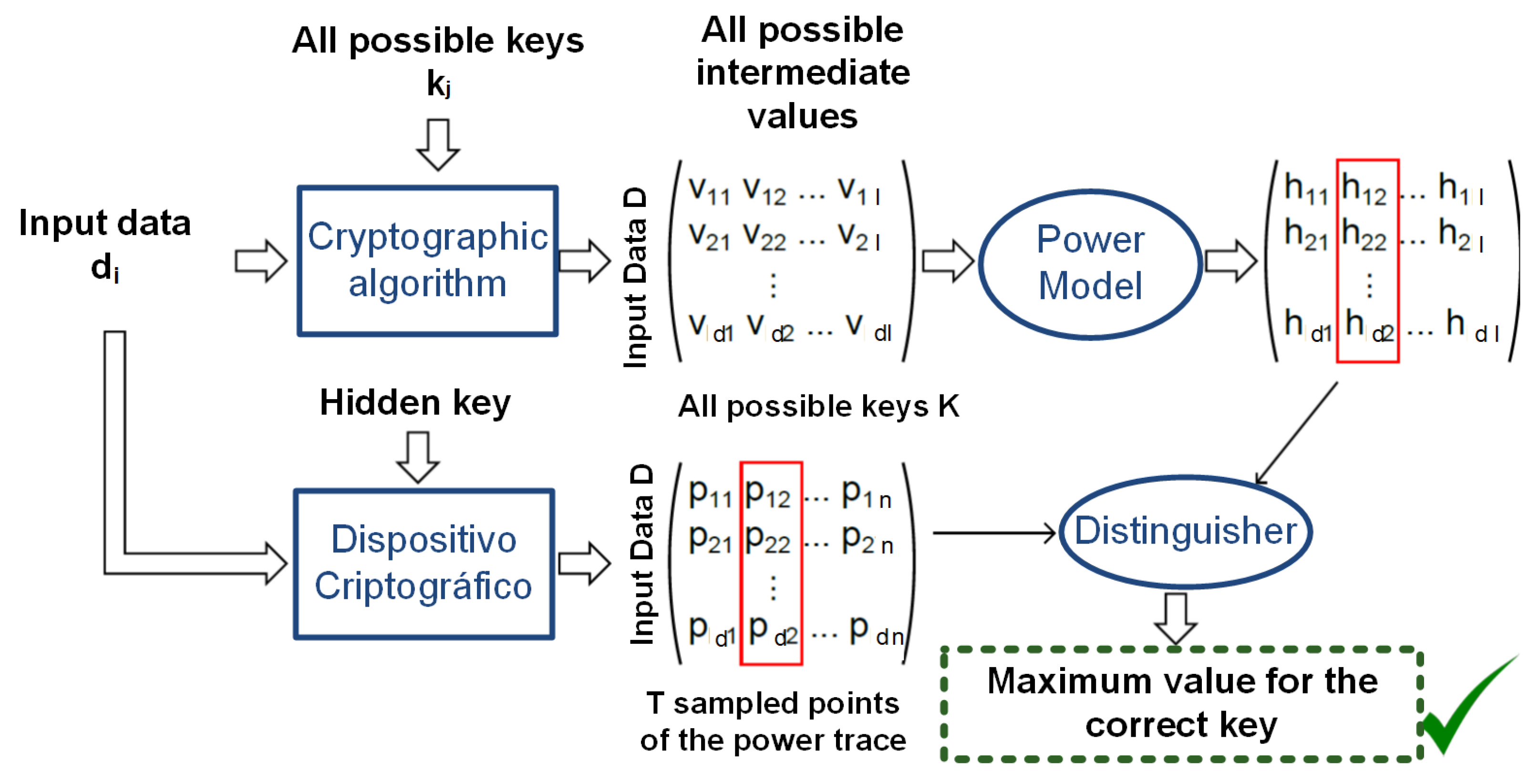
:1. Introduction
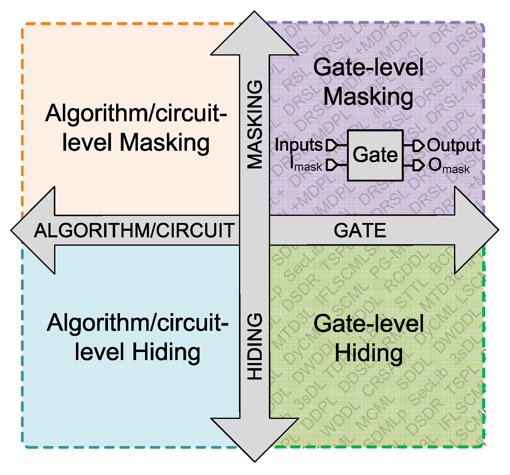
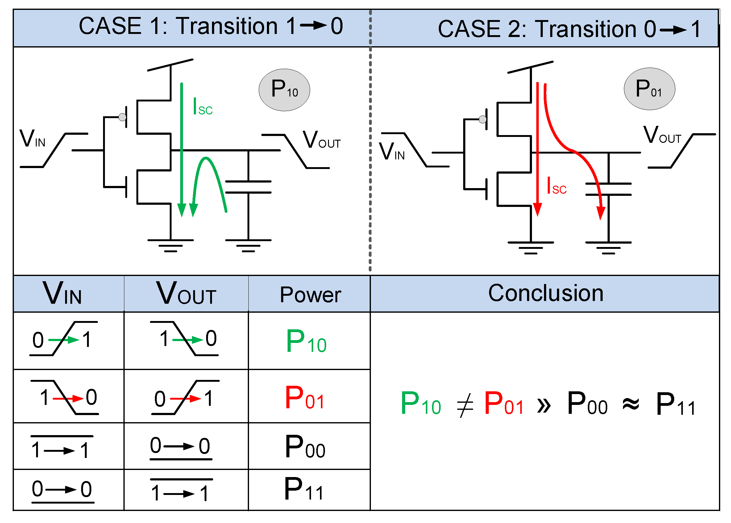
2. Gate-Level Countermeasures against Power Analysis Attacks
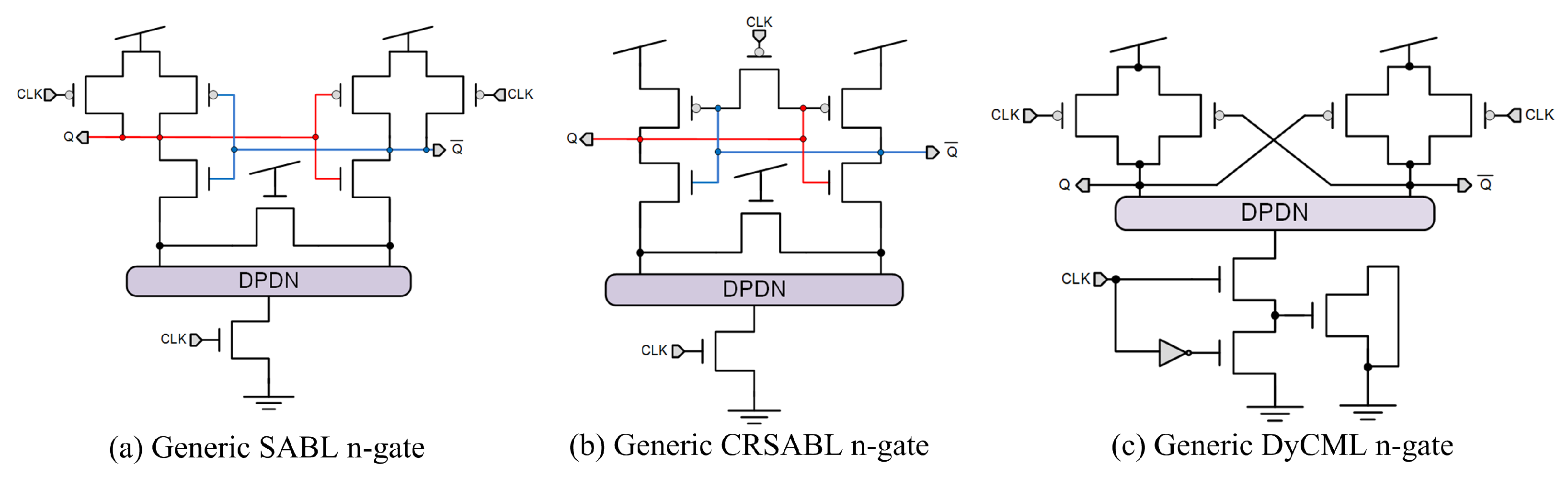
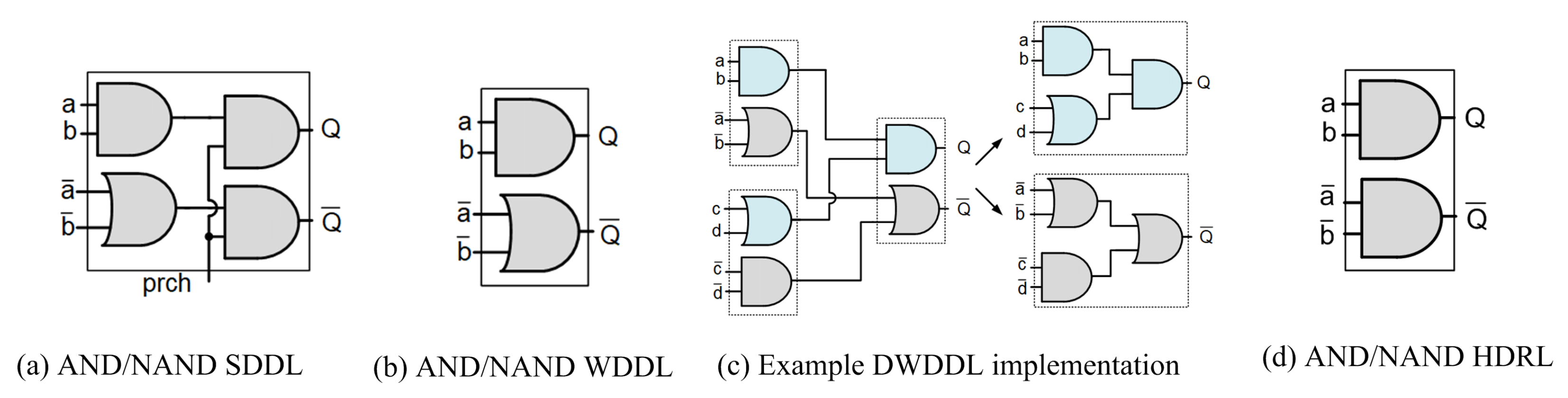
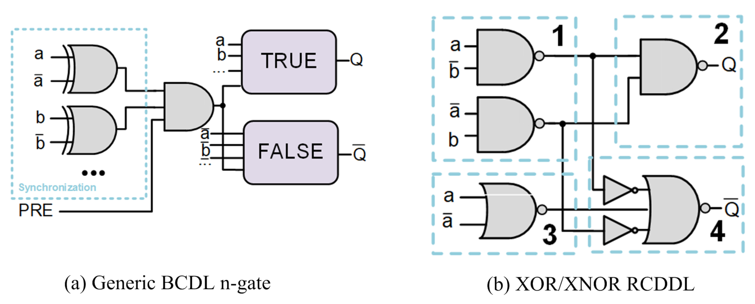
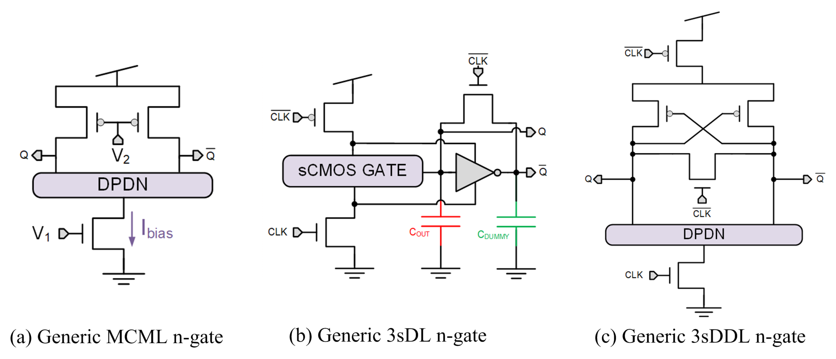
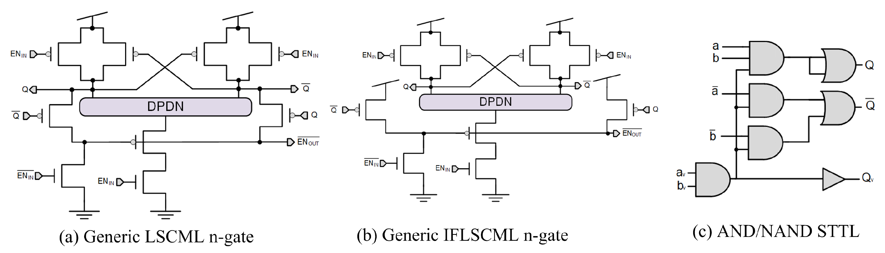
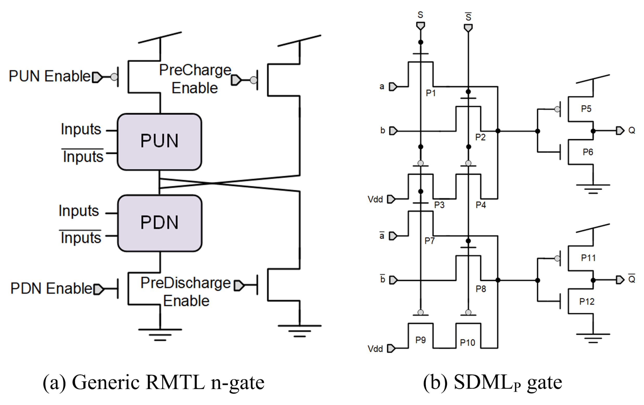
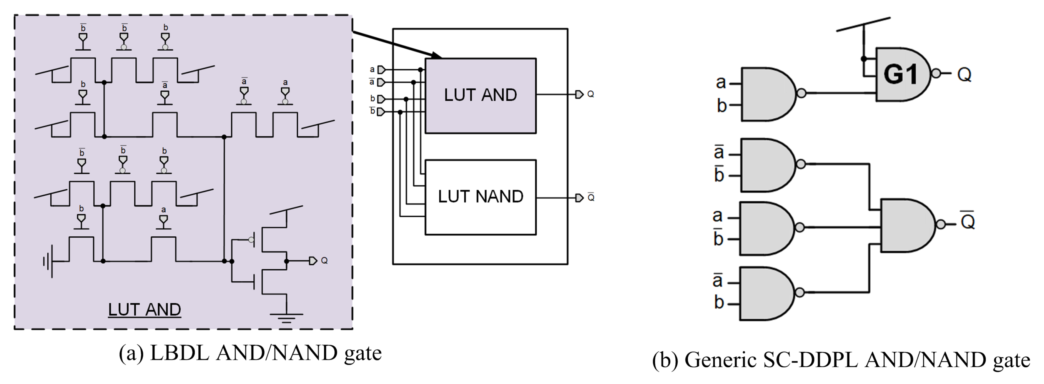
3. Gate-Level Hiding Countermeasures

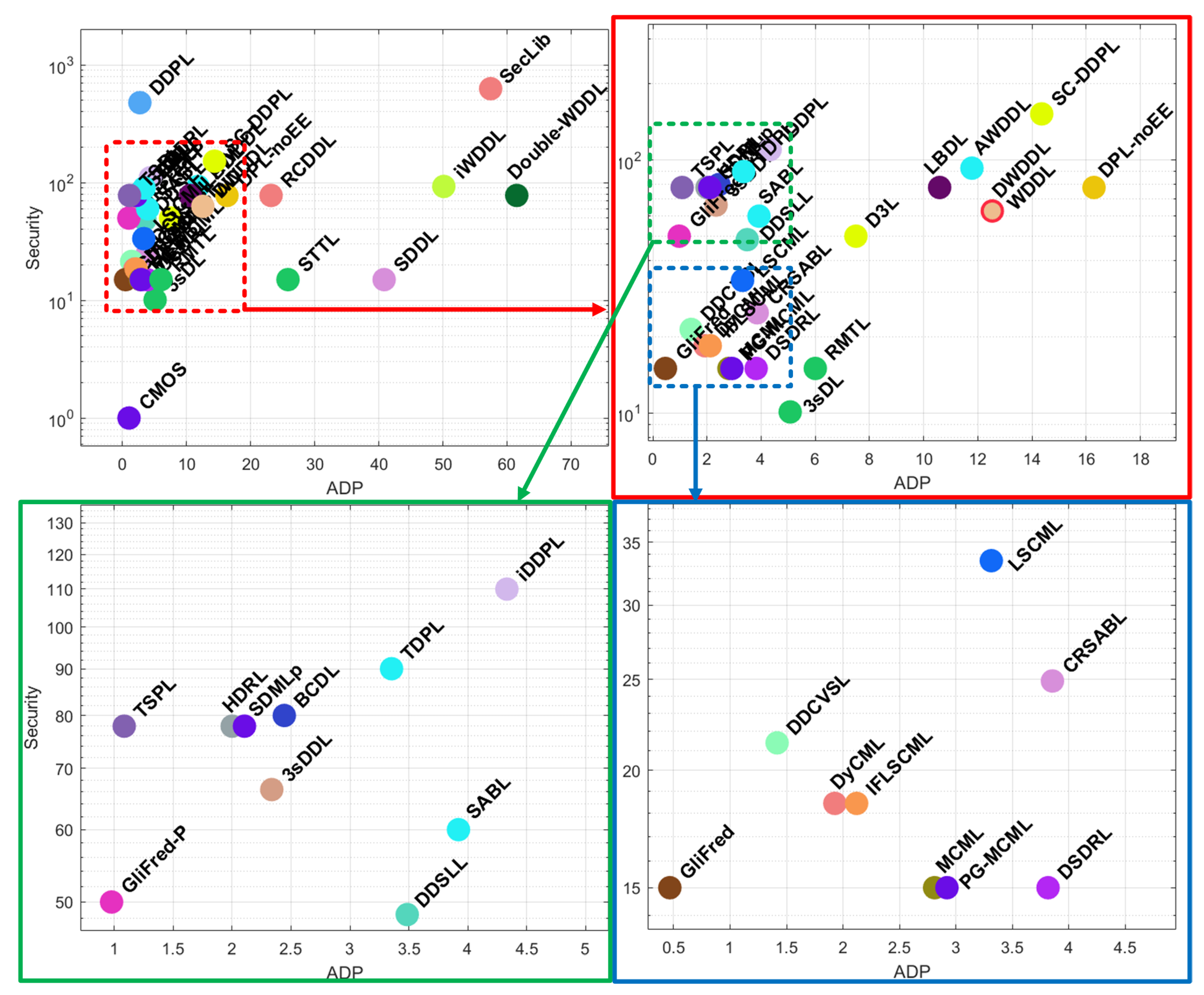
| Logic Style | Data Reference | Based on | Area | Frequency | Power | Security | Special P&R |
|---|---|---|---|---|---|---|---|
| CMOS | NA 1 | STD 2 | 1 | 1 | 1 | 1 | NO |
| 3sDDL [36] | [36] | FC 3 | 2.64 | 1.13 | 3.14 | 47.5–85.25 | YES |
| 3sDL [35] | [35] | FC | 3–4 | 0.67–0.71 | 2.95–3.11 | 7.69–50.78 | YES |
| AWDDL [31] | [31,51] | STD | 4.36 | <WDDL | CMOS | >DPL-noEE | YES |
| BCDL [30] | [30] | STD | 1.71 | 0.70 | NA | >20 | YES |
| CRSABL [14] | [14,59] | FC | 2.12 | 0.55 | 4.56 | 0.38–0.45 × SABL | YES |
| DL [57] | [57,58] | STD | CMOS | CMOS | CMOS | CMOS | NO |
| DDCVSL [44] | [46] | FC | ∼0.8 × DyCML | ∼1.68 × DyCML | ∼2.70 × DyCML | ∼1.16 × DyCML | YES |
| DDPL [39] | [39] | FC | ∼0.75 × SABL | NA | ∼1.86 × SABL | ∼7.97 × SABL | NO |
| DDSLL [60] | [47,60,61] | FC | 1.13–1.45 | 0.37 | 1.37 | >LSCML | YES |
| Double-WDDL [20] | [19,20] | STD | 11.69 | 0.19 | 12 | >WDDL | YES |
| DPL-noEE [26] | [26] | STD | >WDDL | NA | >WDDL | >WDDL | YES |
| DSDRL [24] | [24,25] | STD | 2.08–2.27 | ∼WDDL | ∼2.11–2.27 | >CMOS | NO |
| DWDDL [8] | [8] | STD | ∼WDDL | ∼WDDL | ∼WDDL | ∼WDDL | YES |
| DyCML [15] | [9,15,36,59] | FC | 0.81–2.66 | 0.58–3.7 | 0.47–4.99 | 9.6–27.29 | YES |
| GliFred [51] | [51] | STD | 1.36 | 5.06 | 1.5 | >CMOS | NO |
| GliFred-P [51] | [51] | FC | 4.29 | 5.42 | 1.7 | CMOS | NO |
| HDRL [23] | [23] | STD | 2 | 1 | 2 | >WDDL | NO |
| iDDPL [40] | [40,41] | FC | 3.50 | × SABL | 4.40 | >SABL | NO |
| IFLSCML [47] | [47] | FC | ∼1.10 × DyCML | ∼DyCML | ∼0.77 × DyCML | ∼DyCML | YES |
| iWDDL [22] | [22] | STD | 2 × WDDL | 0.5 × WDDL | ∼2 × WDD | >Double-WDDL | YES |
| LBDL [55] | [55] | STD | 0.98 × WDDL | 1.16 × WDDL | 1.44 × WDDL | >WDDL | YES |
| LSCML [46] | [46] | FC | ∼1.10 × DyCML | ∼0.64 × DyCML | ∼1.09 × DyCML | >DyCML | YES |
| MCML [33] | [33,34] | FC | 2.53 | 0.90 | 2360 | >CMOS | YES |
| PG-MCML [34] | [34] | FC | 2.57 | 0.88 | 0.20 | >CMOS | YES |
| RCDDL [32] | [32] | STD | 3.94 | 0.17 | 3.70 | >WDDL | NO |
| RMTL [50] | [50] | STD | 1.50 | 0.25 | 3.50 | >CMOS | NO |
| SABL [7] | [7,9,36,40,62] | FC | 1.8–3.27 | 0.51 × DyCML | 1.91–7.98 | 14–166 | YES |
| SC-DDPL [56] | [56] | STD | 7.18 | NA | 4.2 | >2.42 × WDDL | NO |
| SDDL [8] | [8,20] | STD | 2 × WDDL | 0.35 | 2 × WDDL | >CMOS | YES |
| SDMLp [54] | [54] | STD | 1.41 | 0.67 | 1.07 | >WDDL | YES |
| SecLib [28] | [28,30,63,64,65] | STD | 15.09–28.00 | 0.25–0.5 | 4.05 | ∼10 × WDDL | NO |
| STTL [49] | [49] | FC/STD | 5.68 | 0.22 | NA | >CMOS | NO |
| TDPL [37] | [37,38] | FC | >SABL | 0.71–0.96 | 1.47–2.83 | >SABL | NO |
| TSPL [38] | [38] | FC | 1.3 | 1.20 | 1.14 | >WDDL | NO |
| WDDL [8] | [8,19,23,30,32,38,54,56,63,64,66,67] | STD | 2.47–11.82 | 0.20–0.94 | 1.70–13.50 | 6.02–119.73 | YES |
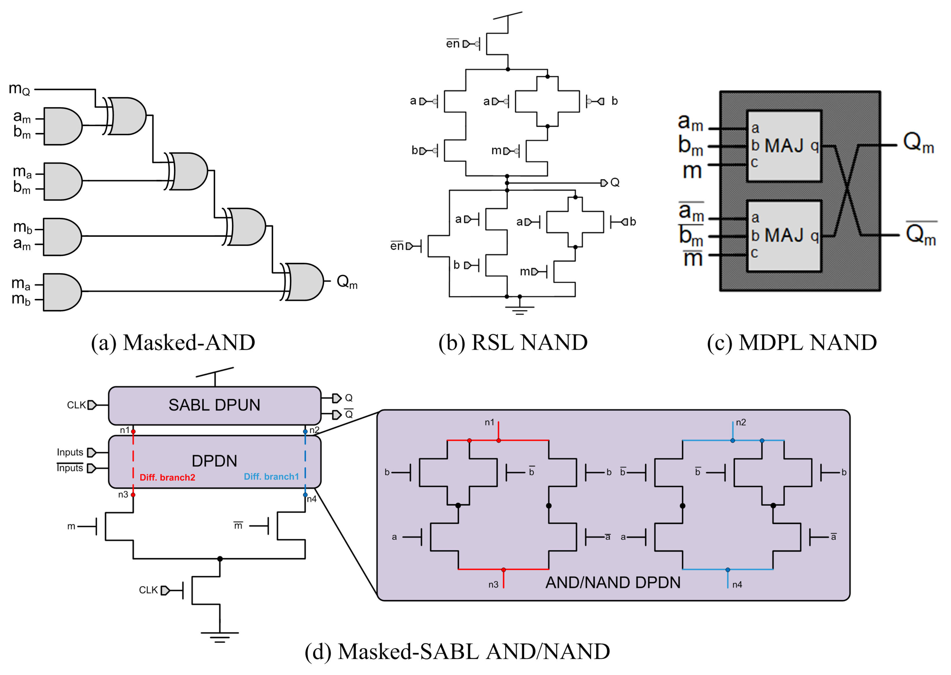
4. Gate-Level Masking
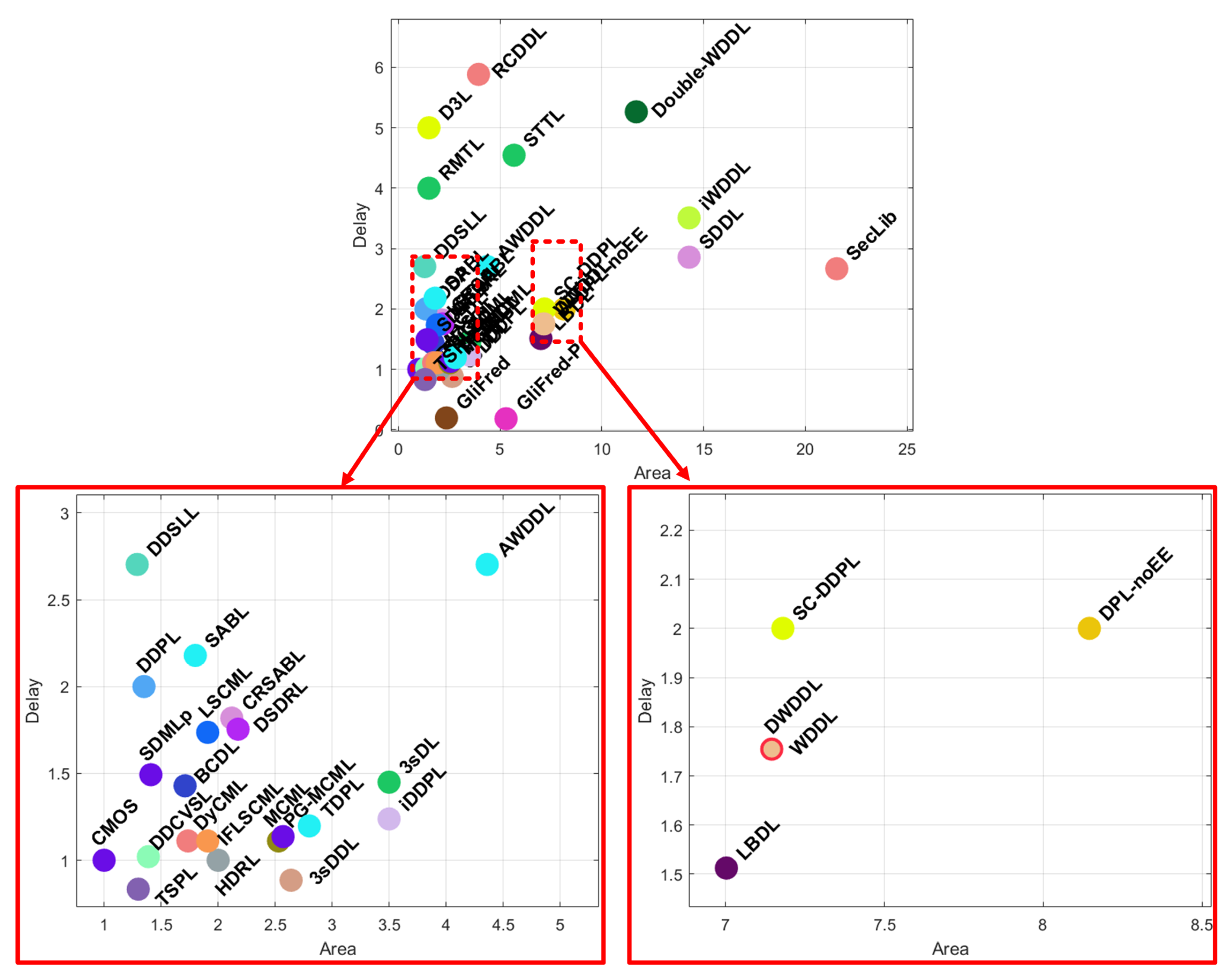
5. Comparative Analysis
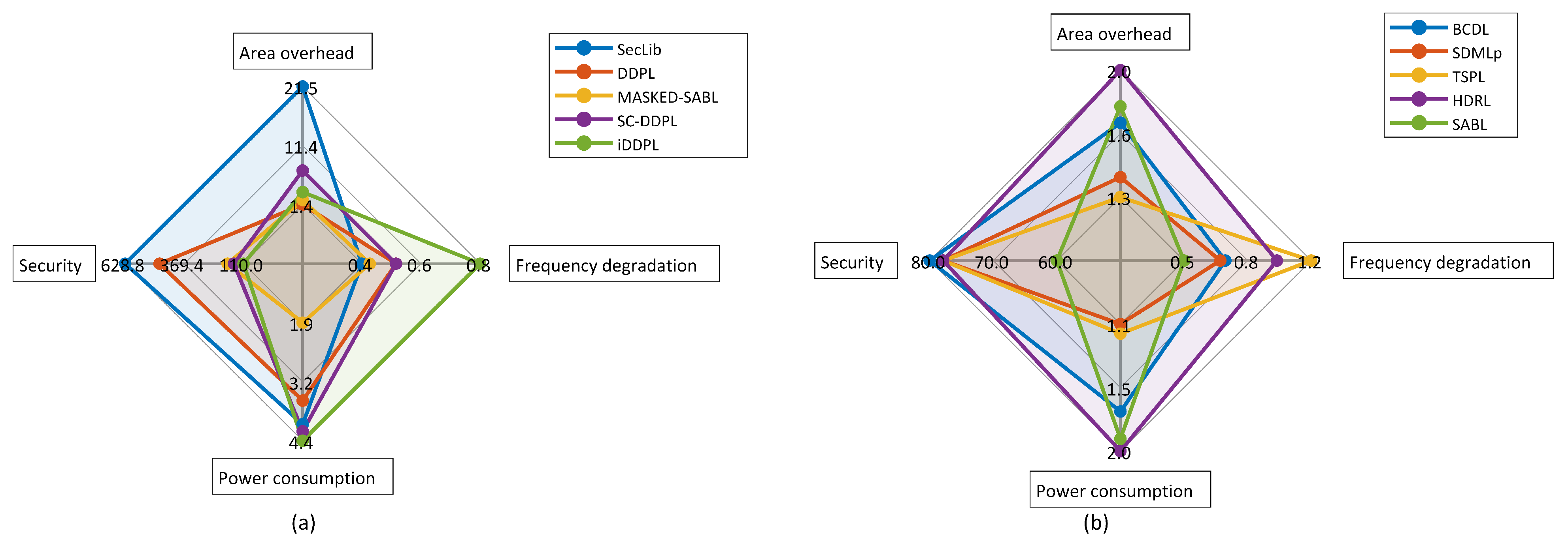
5.1. Gate-Level Hiding
5.2. Gate-Level Masking
6. Conclusions
Author Contributions
Funding
Acknowledgments
Conflicts of Interest
Abbreviations
| 3sDDL | 3-state Differential Dynamic Logic |
| 3sDL | 3-state Dynamic Logic |
| ADP | Area-Delay Product |
| AES | Advanced Encryption Standard |
| ASIC | Application Specific Integrated Circuit |
| AWDDL | Asynchronous Wave Dynamic Differential Logic |
| BCDL | Balanced Cell-based Dual-rail Logic |
| CML | Current Mode Logic |
| CMOS | Complementary Metal-Oxide Semiconductor |
| CPL | Complementary Pass-transistor Logics |
| CRSABL | Charge Recycling Sense Amplifier Based Logic |
| DL | Dual-spacer Dual-rail Delay-insensitive Logic |
| DCVSL | Differential Cascode Voltage Switch Logic |
| DDCVSL | Domino Differential Cascode Voltage Switch Logic |
| DDPL | Delay-based Dual-rail Precharge Logic |
| DDSLL | Dynamic Differential Swing Limited Logic |
| DPA | Differential Power analysis |
| DPDN | Differential Pull Down Network |
| DPL | Dual Precharge Logic |
| DPL-noEE | Dual Precharge Logic with no Early propagation Effect |
| DPUN | Differential Pull Up Network |
| DRC | Design Rule Checking |
| DRSL | Dual-rail Random Switching Logic |
| DSDRL | Dual Spacer Dual-Rail Logic |
| DWDDL | Divided Wave Dynamic Differential Logic |
| DyCML | Dynamic Current Mode Logic |
| EDA | Electronic Design Automation |
| EPDU | Evaluation-Precharge Detection Unit |
| FC | Full-custom |
| FF | Flip Flops |
| FPGA | Field Programmable Gate Array |
| GliFreD | Glitch-Free Duplication |
| GliFred-P | Pipelined fashion Glitch-Free Duplication |
| HDRL | Homogeneous Dual-Rail Logic |
| iDDPL | Improved Delay-based Dual-rail Precharge Logic |
| IFLSCML | Improved Feedback Low Swing Current Mode Logic |
| iMDPL | Improved Masked Dual-rail Precharge Logic |
| IoT | Internet of Things |
| iWDDL | Isolated Wave Dynamic Differential Logic |
| LBDL | Look-up-table Based Differential Logic |
| LSCML | Low Swing Current Mode Logic |
| LUT | Look-Up Table |
| MCML | Metal-Oxide Semiconductor Current Mode Logic |
| MDPL | Masked Dual-rail Precharge Logic |
| MOS | Metal Oxide Semiconductor |
| NMOS | n-channel Metal-Oxide Semiconductor |
| PA | Power Analysis |
| PDN | Pull-Down Network |
| PG-MCML | Power-Gating Metal-Oxide Semiconductor Current Mode Logic |
| PMOS | p-channel Metal-Oxide Semiconductor |
| PUN | Pull-Up Network |
| RCDDL | Reduced Complementary Dynamic and Differential Logic |
| RMTL | Randomized MultiTopology Logic |
| RNG | Random Number Generator |
| RSL | Random Switching Logic |
| RTZ | Return to Zero |
| SABL | Sense Amplifier Based Logic |
| SAFF | StrongArm110 Flip-Flop |
| Sbox | Substitution-box |
| SCA | Side-Channel Attack |
| SC-DDPL | Standard Cell Delay-based Dual-rail Precharge Logic |
| SDMLp | Secure Differential Multiplexer Logic using Pass transistors |
| SecLib | Secure Library |
| SPA | Single Power analysis |
| SDDL | Simple Dynamic Differential Logic |
| STD | Standard |
| STTL | Secure Triple Track Logic |
| TDPL | Three-phase Dual-rail Precharge Logic |
| TEL | Time Enclosed Logic |
| TSPL | Three-phase Single-rail Precharge Logic |
| WDDL | Wave Dynamic Differential Logic |
References
- Mahmoud, R.; Yousuf, T.; Aloul, F.; Zualkernan, I. Internet of things (IoT) security: Current status, challenges and prospective measures. In Proceedings of the 10th International Conference for Internet Technology and Secured Transactions (ICITST’15), London, UK, 14–16 December 2015; pp. 336–341. [Google Scholar]
- Shahverdi, A.; Taha, M.; Eisenbarth, T. Lightweight Side Channel Resistance: Threshold Implementations of Simon. IEEE Trans. Comput. 2017, 66, 661–671. [Google Scholar] [CrossRef]
- Mangard, S.; Oswald, E.; Popp, T. Power Analysis Attacks: Revealing the Secrets of Smart Cards; Springer: Berlin/Heidelberg, Germany, 2007. [Google Scholar]
- Kocher, P. Timing Attacks on Implementations of Diffie-Hellman, RSA, DSS, Other Systems. In Proceedings of the International Cryptology Conference (CRYPTO’96), Barbara, CA, USA, 18–22 August 1996; pp. 104–113. [Google Scholar]
- Kocher, P.; Jaffe, J.; Jun, B. Differential Power Analysis. In Proceedings of the International Cryptology Conference (CRYPTO’99), Barbara, CA, USA, 15–19 August 1999; pp. 388–397. [Google Scholar]
- Hayashi, Y.; Homma, N.; Mizuki, T.; Aoki, T.; Sone, H.; Sauvage, L.; Danger, J.L. Analysis of Electromagnetic Information Leakage From Cryptographic Devices With Different Physical Structures. IEEE Trans. Electromagn. Compat. 2013, 55, 571–580. [Google Scholar] [CrossRef]
- Tiri, K.; Akmal, M.; Verbauwhede, I. A Dynamic and Differential CMOS Logic With Signal Independent Power Consumption to Withstand Differential Power Analysis on Smart Cards. In Proceedings of the 28th European Solid-State Circuits Conference (ESSCIRC’02), Firenze, Italy, 24–26 September 2002; pp. 403–406. [Google Scholar]
- Tiri, K.; Verbauwhede, I.; Hall, B.; Box, P.O.; Angeles, L. A Logic Level Design Methodology for a Secure DPA Resistant ASIC or FPGA Implementation. In Proceedings of the International Conference on Design, Automation and Test in Europe (DATE’04), Paris, France, 16–20 February 2004; pp. 246–251. [Google Scholar]
- Macé, F.; Standaert, F.-X.; Hassoune, I.; Quisquater, J.-J.; Legat, J.-D. A Dynamic Current Mode Logic to Counteract Power Analysis Attacks. In Proceedings of the 19th International Conference on Design of Circuits and Integrated Systems (DCIS’04), Bordeaux, France, 24–26 November 2004; pp. 186–191. [Google Scholar]
- Suzuki, D.; Saeki, M.; Ichikawa, T. Random Switching Logic: A Countermeasure against DPA based on Transition Probability. IACR Cryptology ePrint Archive. 2004, p. 346. Available online: https://eprint.iacr.org/2004/346.pdf (accessed on 1 February 2022).
- Popp, T.; Mangard, S. Masked Dual-Rail Pre-charge Logic: DPA-Resistance Without Routing Constraints. In Proceedings of the International Workshop on Cryptographic Hardware and Embedded Systems (CHES’05), Edinburgh, UK, 29 August–1 September 2005; pp. 172–186. [Google Scholar]
- Messerges, T.S.; Dabbish, E.A.; Puhl, L. Method and Apparatus for Preventing Information Leakage Attacks on a Microelectronic Assembly. U.S. Patent 6,295,606 B1, 25 September 2001. [Google Scholar]
- Nikolic, B.; Oklobdzija, V.G.; Stojanovic, V.; Jia, W.; Chiu, J.K.S.; Leung, M.M.T. Improved Sense-Amplifier-Based Flip-Flop: Design and Measurements. IEEE J. Solid-State Circuits 2000, 35, 876–884. [Google Scholar] [CrossRef]
- Tiri, K.; Verbauwhede, I. Charge Recycling Sense Amplifier Based Logic: Securing Low Power Security IC’s against DPA. In Proceedings of the 30th European Conference on Solid-State Circuits (ESSCIR’04), Leuven, Belgium, 21–23 September 2004; pp. 179–182. [Google Scholar]
- Allam, M.W.; Elmasry, M.I. Dynamic Current Mode Logic (DyCML): A New Low-Power High-Performance Logic Style. J. Solid-State Circuits 2001, 36, 550–558. [Google Scholar] [CrossRef]
- Alioto, M.; Gaetano, P. Model and Design of Bipolar and MOS Current-Mode Logic: CML, ECL and SCL Digital Circuits; Springer: Berlin/Heidelberg, Germany, 2006. [Google Scholar]
- Tiri, K.; Verbauwhede, I. Place and route for secure standard cell design. In Proceedings of the Sixth International Conference on Smart Card Research and Advanced Applications (CARDIS’04), Toulouse, France, 22–27 August 2004; pp. 143–158. [Google Scholar]
- Guilley, S.; Hoogvorst, P.; Mathieu, Y.; Pacalet, R. The Backend Duplication Method A Leakage-Proof Place-and-Route Strategy for ASICs. In Proceedings of the In International Workshop on Cryptographic Hardware and Embedded Systems (CHES’05), Edinburgh, UK, 29 August–1 September 2005; pp. 383–397. [Google Scholar]
- Yu, P.; Schaumont, P. Secure FPGA circuits using controlled placement and routing. In Proceedings of the 5th International Conference on Hardware/Software Codesign and System Synthesis (CODES+ISSS’07), Salzburg, Austria, 30 September 2007; pp. 45–50. [Google Scholar]
- Yu, P. Implementation of DPA-Resistant Circuit for FPGA. Ph.D. Thesis, Virginia Tech, Blacksburg, VA, USA, 2007. [Google Scholar]
- Wild, A.; Moradi, A.; Güneysu, T. Evaluating the duplication of dual-rail precharge logics on FPGAs. In Proceedings of the International Workshop on Constructive Side-Channel Analysis and Secure Design (COSADE’15), Berlin, Germany, 13–14 April 2015; pp. 81–94. [Google Scholar]
- Mcevoy, R.P.; Murphy, C.C.; Marnane, W.P. Isolated WDDL: A Hiding Countermeasure for Differential Power Analysis on FPGAs. ACM Trans. Reconfigurable Technol. Syst. 2009, 2, 3. [Google Scholar] [CrossRef]
- Tanimura, K.; Dutt, N.D. HDRL: Homogeneous dual-rail logic for DPA attack resistive secure circuit design. IEEE Embed. Syst. Lett. 2012, 4, 57–60. [Google Scholar] [CrossRef]
- Sokolov, D.; Murphy, J.; Bystrov, A.; Yakovlev, A. Improving the Security of Dual-Rail Circuits. In Proceedings of the International Workshop on Cryptographic Hardware and Embedded Systems (CHES’04), Cambridge, MA, USA, 11–13 August 2004; pp. 282–297. [Google Scholar]
- Sokolov, D.; Murphy, J.; Bystrov, A.; Yakovlev, A. Design and Analysis of Dual-Rail Circuits for Security Applications. IEEE Trans. Comput. 2005, 54, 449–460. [Google Scholar] [CrossRef]
- Bhasin, S.; Guilley, S.; Flament, F.; Selmane, N.; Danger, J.-L. Countering Early Evaluation: An Approach Towards Robust Dual-Rail Precharge Logic. In Proceedings of the Workshop on Embedded Systems Security (WESS’10), Scottsdale, AZ, USA, 24 October 2010; pp. 1–8. [Google Scholar]
- Suzuki, D.; Saeki, M. Security Evaluation of DPA Countermeasures Using Dual-Rail Pre-charge Logic Style. In Proceedings of the International Workshop on Cryptographic Hardware and Embedded Systems (CHES’06), Yokohama, Japan, 10–13 October 2006; pp. 255–269. [Google Scholar]
- Guilley, S.; Hoogvorst, P.; Mathieu, Y.; Pacalet, R.; Provost, J. CMOS structures suitable for secured hardware. In Proceedings of the International Conference on Design, Automation and Test in Europe (DATE’04), Paris, France, 16–20 February 2004; pp. 1414–1415. [Google Scholar]
- Shams, M.; Ebergen, J.C.; Elmasry, M.I. Modeling and comparing CMOS implementations of the C-element. IEEE Trans. Very Large Scale Integr. (VLSI) Syst. 1998, 6, 563–567. [Google Scholar] [CrossRef]
- Nassar, M.; Bhasin, S.; Danger, J.; Duc, G.; Guilley, S.; Effect, A.E.P. BCDL: A High Speed Balanced DPL for FPGA with Global Precharge and no Early Evaluation. In Proceedings of the Conference on Design, Automation and Test in Europe (DATE’10), Dresden, Germany, 8–12 March 2010; pp. 849–854. [Google Scholar]
- Moradi, A.; Immler, V. Early Propagation and Imbalanced Routing, How to Diminish in FPGAs. In Proceedings of the International Workshop on Cryptographic Hardware and Embedded Systems (CHES’14), Busan, Korea, 23–26 September 2014; pp. 598–615. [Google Scholar]
- Sundaresan, V.; Rammohan, S.; Vemuri, R. Power Invariant Secure IC Design Methodology using Reduced Complementary Dynamic and Differential Logic. In Proceedings of the International Conference on Very Large Scale Integration (VLSI-SoC’07), Atlanta, GA, USA, 15–17 October 2007; pp. 1–6. [Google Scholar]
- Toprak, Z.; Leblebici, Y. Low-Power Current Mode Logic for Improved DPA-Resistance in Embedded Systems. In Proceedings of the International Symposium on Circuits and Systems (ISCAS’05), Kobe, Japan, 26 May 2005; pp. 1059–1062. [Google Scholar]
- Cevrero, A.; Regazzoni, F.; Schwander, M.; Badel, S.; Ienne, P.; Leblebici, Y. Power-gated MOS Current Mode Logic (PG-MCML): A power aware DPA-resistant standard cell library. In Proceedings of the 48th Design Automation Conference (DAC’11), San Diego, CA, USA, 5–9 June 2011; pp. 1014–1019. [Google Scholar]
- Aigner, M.; Mangard, S.; Menicocci, R.; Olivieri, M.; Scotti, G.; Trifiletti, A. A novel CMOS logic style with data independent power consumption. In Proceedings of the International Symposium on Circuits and Systems (ISCAS’05), Kobe, Japan, 26 May 2005; pp. 1066–1069. [Google Scholar]
- Giancane, L.; Marietti, P.; Olivieri, M.; Scotti, G.; Trifiletti, A. A New Dynamic Differential Logic Style as a Countermeasure to Power Analysis Attacks. In Proceedings of the IEEE International Conference on Electronics, Circuits and Systems (ICECS’08), Nabeul, Tunisia, 7–9 November 2008; pp. 364–367. [Google Scholar]
- Bucci, M.; Giancane, L.; Luzzi, R.; Trifiletti, A. Three-Phase Dual-Rail Pre-charge Logic. In Proceedings of the International Workshop on Cryptographic Hardware and Embedded Systems (CHES’06), Yokohama, Japan, 10–13 October 2006; pp. 232–241. [Google Scholar]
- Menendez, E.; Mai, K. Extended Abstract: A High-Performance, Low-Overhead, Power-Analysis-Resistant, Single-Rail Logic Style. In Proceedings of the International Workshop In Hardware-Oriented Security and Trust (HOST’08), Anaheim, CA, USA, 9 June 2008; pp. 33–36. [Google Scholar]
- Bucci, M.; Giancane, L.; Member, S.; Luzzi, R.; Scotti, G.; Trifiletti, A. Delay-Based Dual-Rail Precharge Logic. IEEE Trans. Very Large Scale Integr. Syst. 2011, 19, 1147–1153. [Google Scholar] [CrossRef]
- Bongiovanni, S.; Centurelli, F.; Scotti, G.; Trifiletti, A. Design and validation through a frequency-based metric of a new countermeasure to protect nanometer ICs from side-channel attacks. J. Cryptogr. Eng. 2015, 5, 269–288. [Google Scholar] [CrossRef]
- Bellizia, D.; Scotti, G.; Trifiletti, A. TEL Logic Style as a Countermeasure Against Side-Channel Attacks: Secure Cells Library in 65nm CMOS and Experimental Results. IEEE Trans. Circuits Syst. I Regul. Pap. 2018, 65, 3874–3884. [Google Scholar] [CrossRef]
- Tiri, K.; Verbauwhede, I. Design method for constant power consumption of differential logic circuits. In Proceedings of the Design, Automation and Test in Europe (DATE’05), Munich, Germany, 7–11 March 2005; pp. 628–633. [Google Scholar]
- Tena-Sánchez, E.; Castro, J.; Acosta, A.J. A methodology for optimized design of secure differential logic gates for DPA resistant circuits. IEEE J. Emerg. Sel. Top. Circuits Syst. 2014, 4, 203–215. [Google Scholar] [CrossRef] [Green Version]
- Ng, P.; Balsara, P.T.; Steiss, D. Performance of CMOS differential circuits. IEEE J. Solid-State Circuits 1996, 31, 841–846. [Google Scholar] [CrossRef]
- Chu, K.M.; Pulfrey, D.L. Design procedures for differential cascode voltage switch circuits. IEEE J. Solid-State Circuits 1986, 21, 1082–1087. [Google Scholar] [CrossRef] [Green Version]
- Hassoune, I.; Mace, F.; Flandre, D.; Legat, J.-D. Low-swing current mode logic (LSCML): A new logic style for secure and robust smart cards against power analysis attacks. Microelectron. J. 2006, 37, 997–1006. [Google Scholar] [CrossRef]
- Hassoune, I.; Mace, F.; Flandre, D.; Legat, J.D. Dynamic differential self-timed logic families for robust and low-power security ICs. Integr. VLSI J. 2007, 40, 355–364. [Google Scholar] [CrossRef]
- Razafindraibe, A.; Robert, M.; Maurine, P. Formal evaluation of the robustness of dual-rail logic against DPA attacks. In Proceedings of the International Workshop on Power and Timing Modeling, Optimization and Simulation (PATMOS’06), Montpellier, France, 13–15 September 2006; pp. 634–644. [Google Scholar]
- Soares, R.; Calazans, N.; Lomné, V.; Maurine, P.; Torres, L.; Robert, M. Evaluating the Robustness of Secure Triple Track Logic through Prototyping. In Proceedings of the 21st Annual Symposium on Integrated Circuits and System Design (SBCCI’08), Gramado, Brazil, 1–4 September 2008; pp. 193–198. [Google Scholar]
- Avital, M.; Dagan, H.; Keren, O.; Fish, A. Randomized Multitopology Logic Against Differential Power Analysis. IEEE Trans. Very Large Scale Integr. Syst. 2015, 23, 702–711. [Google Scholar] [CrossRef]
- Wild, A.; Moradi, A.; Tim, G. GliFreD: Glitch-Free Duplication Towards Power-Equalized Circuits on FPGAs. IEEE Trans. Comput. 2018, 67, 375–387. [Google Scholar] [CrossRef]
- Moradi, A.; Mischke, O. Glitch-free implementation of masking in modern FPGAs. In Proceedings of the IEEE International Symposium Hardware-Oriented Security and Trust (HOST’12), San Francisco, CA, USA, 3–4 June 2012; pp. 89–95. [Google Scholar]
- He, W.; Otero, A.; Torre, E.D.L.; Riesgo, T. Automatic generation of identical routing pairs for FPGA implemented DPL logic. In Proceedings of the International Conference on Reconfigurable Computing and FPGAs (ReConFig’12), Cancun, Mexico, 9–11 December 2012; pp. 1–6. [Google Scholar]
- Ramakrishnan, L.N.; Chakkaravarthy, M.; Manchanda, A.S. SDMLp: On the Use of Complementary Pass Transistor Logic for Design of DPA Resistant Circuits. In Proceedings of the International Symposium on Hardware-Oriented Security and Trust (HOST’12), San Francisco, CA, USA, 3–4 June 2012; pp. 31–36. [Google Scholar]
- Vue, D. A Look-Up-Table Based Differential Logic to Counteract DPA Attacks. In Proceedings of the 8th International Conference on ASIC (ASICON’09), Changsha, China, 20–23 October 2009; pp. 855–858. [Google Scholar]
- Bellizia, D.; Bongiovanni, S.; Olivieri, M.; Scotti, G. SC-DDPL: A Novel Standard-Cell Based Approach for Counteracting Power Analysis Attacks in the Presence of Unbalanced Routing. IEEE Trans. Circuits Syst. I Regul. Pap. 2020, 67, 2317–2330. [Google Scholar] [CrossRef]
- Cilio, W.; Linder, M.; Porter, C.; Di, J.; Smith, S.; Thompson, D. Side-channel attack mitigation using dual-spacer Dual-rail Delay-insensitive Logic (D3L). In Proceedings of the IEEE SoutheastCon (SoutheastCon’10), Charlotte, NC, USA, 18–21 March 2010; pp. 471–474. [Google Scholar]
- Cilio, W.; Linder, M.; Porter, C.; Di, J.; Smith, S.; Thompson, D. Mitigating power-and timing-based side-channel attacks using dual-spacer dual-rail delay-insensitive asynchronous logic. Microelectron. J. 2013, 44, 258–269. [Google Scholar] [CrossRef]
- Sundström, T.; Alvandpour, A. A comparative analysis of logic styles for secure IC’s against DPA attacks. In Proceedings of the NORCHIP Conference (NORCHIP’05), Oulu, Finland, 21–22 November 2005; pp. 297–300. [Google Scholar]
- Kamel, D.; Renauld, M.; Bol, D.; Standaert, F.-X.; Flandre, D. Analysis of Dynamic Differential Swing Limited Logic for Low-Power Secure Applications. J. Low Power Electron. Appl. 2012, 2, 98–126. [Google Scholar] [CrossRef] [Green Version]
- Renauld, M.; Kamel, D.; Standaert, F.X.; Flandre, D. Information Theoretic and Security Analysis of a 65-Nanometer DDSLL AES S-Box. In Cryptographic Hardware and Embedded Systems (CHES’11); Lecture Notes in Computer Science; Springer: Berlin/Heidelberg, Germany, 2011; Volume 6917. [Google Scholar]
- Tiri, K.; Verbauwhede, I. Securing Encryption Algorithms against DPA at the Logic Level: Next Generation Smart Card Technology. In InInternational Workshop on Cryptographic Hardware and Embedded Systems; Lecture Notes in Computer Science; Springer: Berlin/Heidelberg, Germany, 2003; Volume 2779, pp. 125–136. [Google Scholar]
- Guilley, S.; Flament, F.; Hoogvorst, P.; Pacalet, R.; Mathieu, Y. Secured CAD back-end flow for power-analysis-resistant cryptoprocessors. IEEE Des. Test Comput. 2007, 24, 546–555. [Google Scholar] [CrossRef]
- Guilley, S.; Sauvage, L.; Hoogvorst, P.; Pacalet, R.; Bertoni, G.M.; Chaudhuri, S. Security Evaluation of WDDL and SecLib Countermeasures against Power Attacks. IEEE Trans. Comput. 2008, 57, 1482–1497. [Google Scholar] [CrossRef]
- Guilley, S.; Sauvage, L.; Flament, F.; Vong, V.; Hoogvorst, P.; Pacalet, R. Evaluation of Power Constant Dual-Rail Logics Countermeasures against DPA with Design Time Security Metrics. IEEE Trans. Comput. 2010, 59, 1250–1263. [Google Scholar] [CrossRef]
- Wang, H.; Tiri, K.; Hodjat, A. AES-based security coprocessor IC in 0.18 μm CMOS with resistance to differential power analysis side channel attack. IEEE J. Solid-State Circuits 2006, 41, 781–791. [Google Scholar] [CrossRef] [Green Version]
- Rammohan, S.; Sundaresan, V.; Vemuri, R. Reduced complementary dynamic and differential logic: A CMOS logic style for DPA-resistant secure IC design. In Proceedings of the IEEE International Frequency Control Symposium and Exposition, Miami, FL, USA, 4–7 June 2008; pp. 699–705. [Google Scholar]
- Chaves, R.; Chmielewski, Ł.; Regazzoni, F.; Batina, L. SCA-Resistance for AES: How Cheap Can We Go? In Proceedings of the International Conference on Cryptology in Africa, Cairo, Egypt, 9–11 July 2018; pp. 107–123. [Google Scholar]
- Golic, J.D.; Menicocci, R. Universal masking on logic gate level. IEEE Electron. Lett. 2004, 37, 898–899. [Google Scholar] [CrossRef]
- Golic, J.D. Techniques for random masking in hardware. IEEE Trans. Circuits Syst. I Regul. Pap. 2007, 54, 291–300. [Google Scholar] [CrossRef]
- Trichina, E. Combinational Logic Design for AES Subbyte transformation on Masked Data. IACR Cryptology ePrint Archive. 2003, p. 236. Available online: https://eprint.iacr.org/2003/236.pdf (accessed on 1 February 2022).
- Trichina, E.; Korkishko, T.; Lee, K.H. Small Size, Low Power, Side Channel-Immune AES Coprocessor: Design and Synthesis Results. In Proceedings of the International Conference on Advanced Encryption Standard, Bonn, Germany, 10–12 May 2004; pp. 113–127. [Google Scholar]
- Mangard, S.; Popp, T.; Gammel, B.M. Side-channel leakage of masked CMOS gates. In Proceedings of the Cryptographers’ Track at the RSA Conference, San Francisco, CA, USA, 14–18 February 2005; pp. 351–365. [Google Scholar]
- Fischer, W.; Gammel, B.M. Masking at Gate Level in the Presence of Glitches. In Proceedings of the International Workshop on Cryptographic Hardware and Embedded Systems (CHES’05), Edinburgh, UK, 29 August–1 September 2005; pp. 187–200. [Google Scholar]
- Moradi, A.; Kirschbaum, M.; Eisenbarth, T.; Paar, C. Masked Dual-Rail Precharge Logic Encounters State-of-the-Art Power Analysis Methods. IEEE Trans. Very Large Scale Integr. Syst. 2012, 20, 578–1589. [Google Scholar] [CrossRef] [Green Version]
- Popp, T.; Kirschbaum, M.; Zefferer, T.; Mangard, S. Evaluation of the Masked Logic Style MDPL on a Prototype Chip. In Proceedings of the International Workshop on Cryptographic Hardware and Embedded Systems (CHES’07), Vienna, Austria, 10–13 September 2007; pp. 81–94. [Google Scholar]
- Tiri, K.; Schaumont, P. Changing the odds against Masked Logic. In Proceedings of the International Workshop on Selected Areas in Cryptography, Montreal, QC, Canada, 17–18 August 2006; pp. 134–146. [Google Scholar]
- Chen, Z.; Zhou, Y. Dual-Rail Random Switching Logic: A Countermeasure to Reduce Side Channel Leakage. In Proceedings of the International Workshop on Cryptographic Hardware and Embedded Systems (CHES’06), Yokohama, Japan, 10–13 October 2006; pp. 242–254. [Google Scholar]
- Danger, J.; Guilley, S.; Bhasin, S.; Nassar, M. Overview of Dual Rail with Precharge Logic Styles to Thwart Implementation-Level Attacks on Hardware Cryptoprocessors. In Proceedings of the International Conference on Signals, Circuits and Systems (SCS’09), Medenine, Tunisia, 6–8 November 2009; pp. 1–8. [Google Scholar]
- Kirschbaum, M.; Popp, T. Evaluation of a DPA-Resistant Prototype Chip. In Proceedings of the Annual Computer Security Applications Conference (ACSAC’09), Washington, DC, USA, 7–11 December 2009; pp. 43–50. [Google Scholar]
- Fadaeinia, B.; Anik, M.T.H.; Karimi, N.; Moradi, A. Masked SABL: A Long Lasting Side-Channel Protection Design Methodology. IEEE Access 2021, 9, 90455–90464. [Google Scholar] [CrossRef]
- Schaumont, P.; Tiri, K. Masking and Dual-Rail Logic Don’t Add Up. In Proceedings of the International Workshop on Cryptographic Hardware and Embedded Systems (CHES’07), Vienna, Austria, 10–13 September 2007; pp. 95–106. [Google Scholar]
- Popp, T.; Thomaspoppiaiktugrazat, E.; Mangard, S. Implementation Aspects of the DPA-Resistant Logic Style MDPL D-fitipfloDPs. In Proceedings of the International Symposium on Circuits and Systems (ISCAS’06), Singapore, 4–7 December 2006; pp. 2913–2916. [Google Scholar]


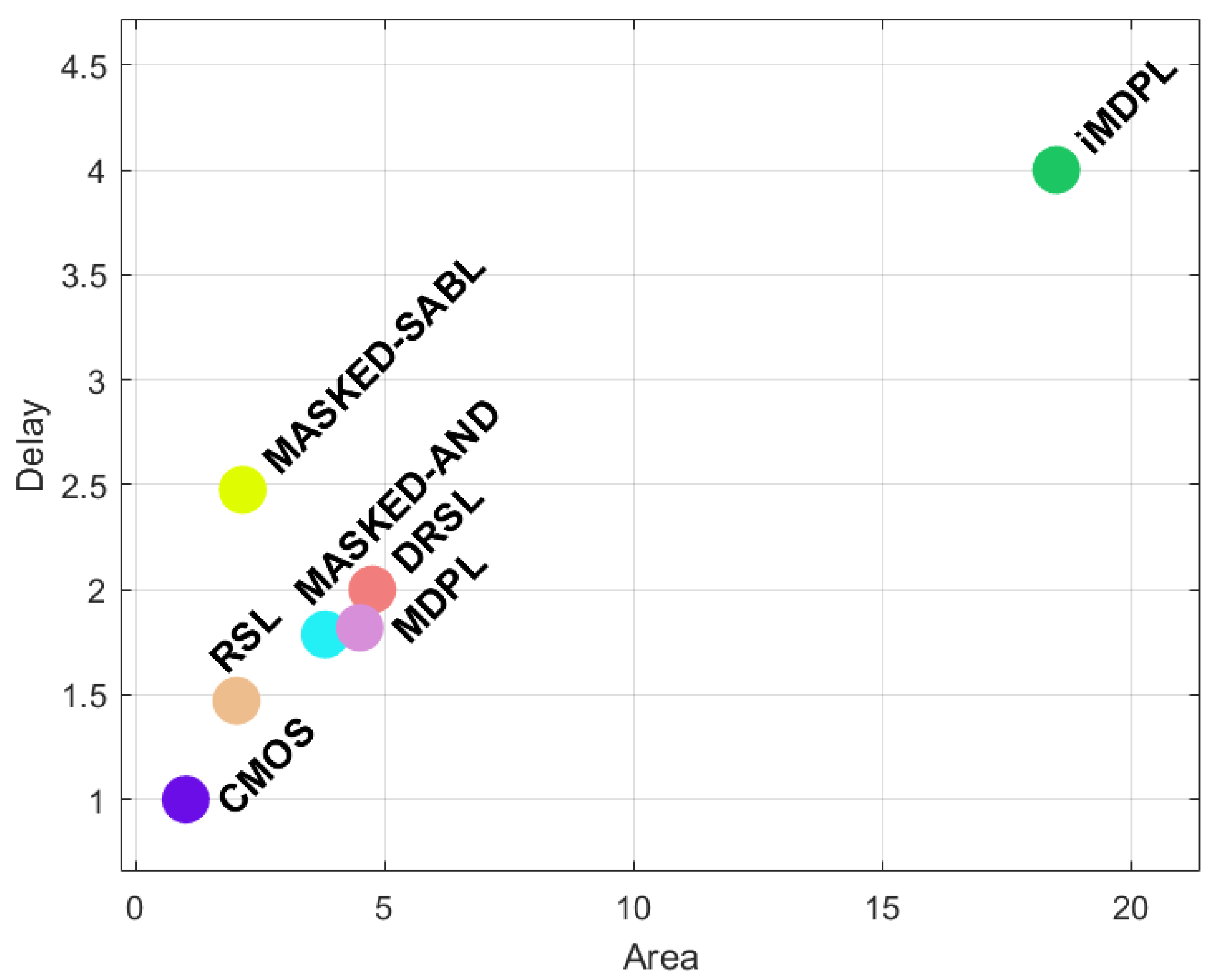
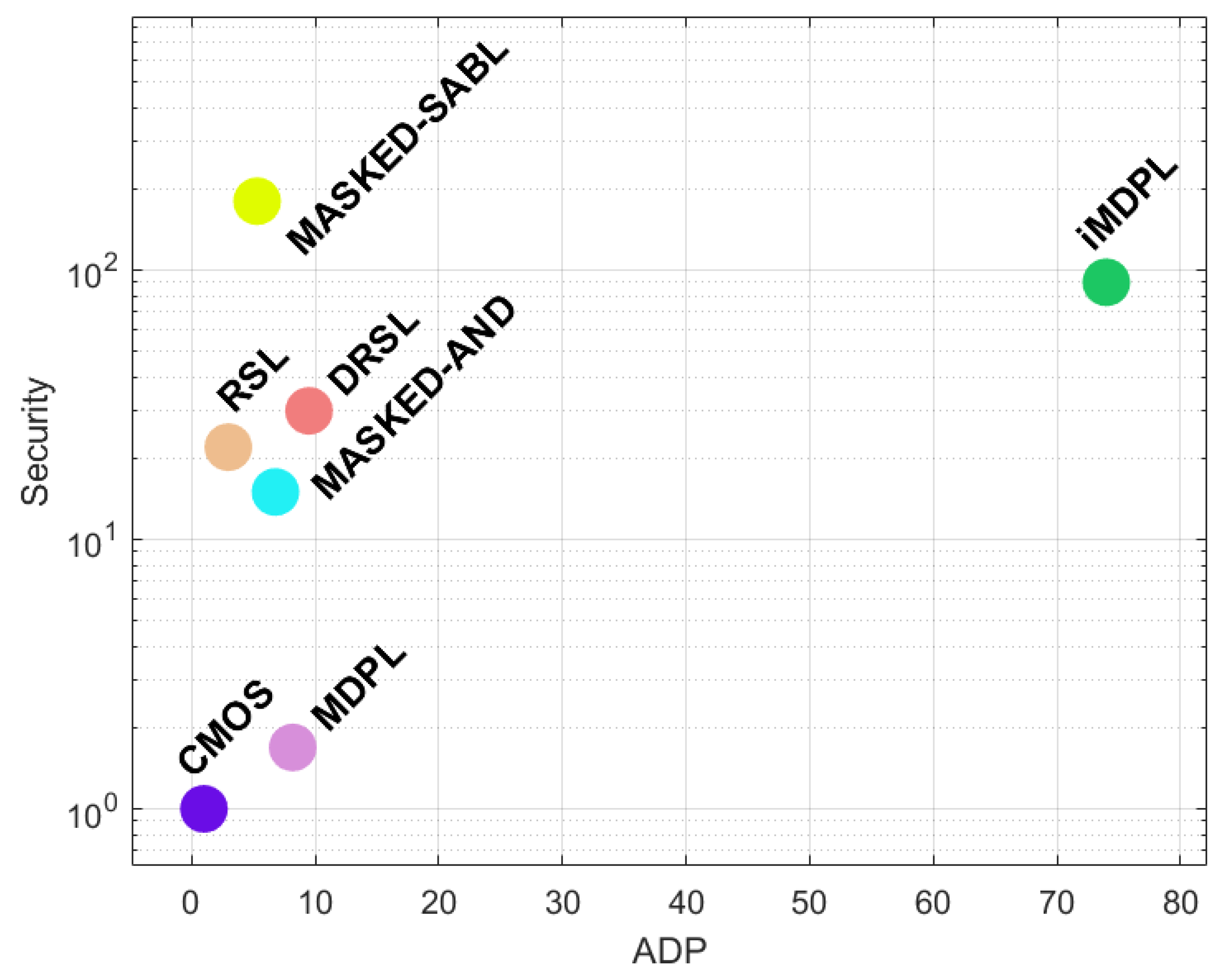
| Logic Style | Data Reference | Based on | Area | Frequency | Power | Security | Special P&R |
|---|---|---|---|---|---|---|---|
| CMOS | NA 1 | STD | 1 | 1 | 1 | 1 | NO |
| DRSL [78] | [78,79] | FC/STD 2 | 2–7.5 | 0.50 | >CMOS | >MDPL 3 | NO |
| iMDPL [76] | [80] | STD | 18–19 | 0.2–0.3 | >MDPL | 90–120 | NO |
| MASKED-AND [71] | [10] | STD | 3.86 | 0.56 | NA | >CMOS 4 | NO |
| Masked-SABL [81] | [81] | FC | 1.19 × SABL | 0.88 × SABL | =SABL | 3 × SABL | YES |
| MDPL [11] | [11,76,83] | STD | 4–5 | 0.5–0.6 | 17.43 | 1.69 | NO |
| RSL [10] | [10] | FC/STD 2 | 2.02 | 0.68 | NA | >MASKED-AND 4 | NO |
Publisher’s Note: MDPI stays neutral with regard to jurisdictional claims in published maps and institutional affiliations. |
© 2022 by the authors. Licensee MDPI, Basel, Switzerland. This article is an open access article distributed under the terms and conditions of the Creative Commons Attribution (CC BY) license (https://creativecommons.org/licenses/by/4.0/).
Share and Cite
Tena-Sánchez, E.; Potestad-Ordóñez, F.E.; Jiménez-Fernández, C.J.; Acosta, A.J.; Chaves, R. Gate-Level Hardware Countermeasure Comparison against Power Analysis Attacks. Appl. Sci. 2022, 12, 2390. https://doi.org/10.3390/app12052390
Tena-Sánchez E, Potestad-Ordóñez FE, Jiménez-Fernández CJ, Acosta AJ, Chaves R. Gate-Level Hardware Countermeasure Comparison against Power Analysis Attacks. Applied Sciences. 2022; 12(5):2390. https://doi.org/10.3390/app12052390
Chicago/Turabian StyleTena-Sánchez, Erica, Francisco Eugenio Potestad-Ordóñez, Carlos J. Jiménez-Fernández, Antonio J. Acosta, and Ricardo Chaves. 2022. "Gate-Level Hardware Countermeasure Comparison against Power Analysis Attacks" Applied Sciences 12, no. 5: 2390. https://doi.org/10.3390/app12052390
APA StyleTena-Sánchez, E., Potestad-Ordóñez, F. E., Jiménez-Fernández, C. J., Acosta, A. J., & Chaves, R. (2022). Gate-Level Hardware Countermeasure Comparison against Power Analysis Attacks. Applied Sciences, 12(5), 2390. https://doi.org/10.3390/app12052390