Article

Evolution of System Embedded Optical Interconnect in Sub-Top-of-Rack Data Center Systems

1
School of Physics and Astronomy, University of St Andrews, St Andrews KY16 9AJ, UK
2
Seagate Research Group, Seagate Technology, Shakopee, MN 55379, USA
3
Resolute Photonics Ltd., Eastleigh SO53 3AL, UK
4
Centre for Advanced Photonics and Process Analysis (CAPPA), Munster Technology University, T12 P928 Cork, Ireland
5
WaveOptics Ltd., Abingdon OX14 4SR, UK
6
Seagate Systems UK Ltd., Havant PO9 1SA, UK
*
Author to whom correspondence should be addressed.
Retired.
Deceased.
Appl. Sci. 2022, 12(3), 1565; https://doi.org/10.3390/app12031565
Submission received: 18 October 2021 / Revised: 9 December 2021 / Accepted: 14 December 2021 / Published: 31 January 2022
(This article belongs to the Collection New Trends in Optical Networks)

Abstract

:
In this paper we review key technological milestones in system embedded optical interconnects in data centers that have been achieved between 2014 and 2020 on major European Union research and development projects. This includes the development of proprietary optically enabled data storage and switch systems and optically enabled data storage and compute subsystems. We report on four optically enabled data center system demonstrators: LightningValley, ThunderValley2, Pegasus and Aurora, which include advanced optical circuits based on polymer waveguides and fibers and proprietary electro-optical connectors. We also report on optically enabled subsystems including Ethernet-connected hard disk drives and microservers. Both are designed in the same pluggable carrier form factor and with embedded optical transceiver and connector interfaces, thus allowing, for the first time, both compute and storage nodes to be optically interchangeable and directly interconnectable over long distances. Finally, we present the Nexus platform, which allows different optically enabled data center test systems and subsystems to be interconnected and comparatively characterized within a data center test environment.

1. Introduction

The past decade is exemplified by the surge in digital information being captured, processed, stored and moved from one location to another. This data explosion has been precipitated for the most part by the widespread adoption of mobile data devices—predominantly smartphones and tablets—and is pushing modern information and communications systems beyond their design limits and towards a crippling “data cliff”.
A major consequence of the adoption of smaller portable mobile data devices over larger static computer terminals (PCs) is that a dramatic shift is now occurring in where customers need to store their information. While it was sufficient to store data locally (such as on the user’s local laptop or desktop computer hard drive), the average size of data objects generated, such as high-definition pictures or short videos, has grown to the extent that the storage available on mobile devices is rapidly becoming insufficient for long-term accumulation and retention of data. This has given rise to the emergence of “cloud” services where customers can outsource their data storage and increased computing requirements to very large and secure data centers typically comprising at least 100,000 servers and associated data storage and network switching. These “hyperscale” data centers are run by internet content providers (ICPs) such as Amazon, Google and Microsoft and provide the dedicated compute, storage and server equipment required to meet the remote and diverse data processing and storage requirements of cloud environments. However, in order to cope with rapidly changing customer demand, the architectures underlying the data centers themselves need to evolve, and a critical part of that evolution is the deployment of optical connections at all levels of the data center environment.
Printed circuit boards (PCBs) are at the heart of all modern information and communication technology (ICT) systems. The increase in data communication speeds incurs a toll on ICT systems, such as servers and switches, when higher frequency electronic signals are conveyed along the metal channels used in conventional PCBs. As frequencies of these electronic signals increase, dielectric absorption, skin effect and other resistive loss mechanisms attenuate them more strongly, while signal reflections, signal skew and interference from other electronic channels distort their integrity. Furthermore, the environmental effects of system operation, such as temperature and humidity, cause changes in the circuit board substrate, thus altering the carefully balanced characteristics of the electronic channels. Many of these constraints can be mitigated to some degree, however, at an ever-mounting cost to the overall system design and with an increasing power penalty.
Embedded optical interconnect technologies, whether deployed at the cable level, circuit board level or chip level, offer significant performance and power advantages over conventional electronic interconnect. Performance gains include higher data rates, reduced electromagnetic interference, reduced power consumption, higher channel density and a corresponding reduction in the amount of cable or PCB materials used. Therefore, in order to cope with the exponential increase in capacity, processing power and bandwidth density inside information communication systems, there has been a trend over the past decade to migrate optical channels down from the higher communication tier optical fiber networks into the data communication system enclosure itself. One area in which this is particularly apparent is in modern data centers, where the migration of optical interconnect into top-of-rack (TOR) or other network switch enclosures can substantially mitigate the communications bottlenecks resulting from the increase in both data rate and internal interconnect link lengths. As is discussed toward the end of the paper, a great deal of research is currently underway into “copackaged optics” (CPO) for data center switch ASICs, which have aggregated bandwidths expected to exceed 100 Tb/s by 2026. Intel has been leading the effort to develop CPO based on silicon photonics microtransceivers or “chiplets” coassembled with switch ASICs onto common carriers [1,2,3] to accommodate these astronomical bandwidths in data center switch ASICs. However, the vast majority of systems in data centers, what we refer to as sub-TOR systems, are servers and data storage arrays, which in hyperscale data centers number in the hundreds of thousands.
In order to assess the viability of embedding optical links within modern sub-TOR data center architectures, three generations of data center systems were developed over the past 5 years based on current storage switch enclosure form factors. In this paper, we review the evolution of system embedded optical interconnect technologies in three key data center demonstration prototype platforms produced by Seagate Systems in the UK: LightningValley, ThunderValley2 and Pegasus, which were adapted from different data storage switch enclosures to allow selected internal high-speed electronic transmission lines to be converted to optical links.
LightningValley is a partially optically interconnected data storage system. It was developed based on a modified 4U24 OneStor enclosure from Seagate Technology, in which 12 Gb/s Serial Attached SCSI (SAS) traffic was conveyed optically between the SAS protocol switches on two internal controller cards along 24 PCB embedded polymer optical waveguide channels, thereby showing, for the first time, how in-system optical channels could be successfully deployed within a 12G SAS architecture [4].
ThunderValley2 is a fully optically enabled data storage array that was developed based on a 2U24 OneStor enclosure from Seagate Technology, in which all internal high-speed links were implemented optically. This required the deployment of commercial midboard optical transceivers, an electro-optical midplane and proprietary pluggable optical connectors for hard disk drives [5].
Pegasus is a fully optically enabled 24 drive Ethernet data storage, switch and compute platform, for which interchangeable optical transceiver mezzanine cards and a proprietary electro-optical drive connector were developed.
Aurora is a test and measurement platform developed to allow comparative characterization of different types of more advanced optical interconnect technologies including embedded and discrete polymer and glass waveguide circuits, optical PCB connectors and transceiver and switch technologies including advanced silicon photonics devices [6].
A converged data center test rack, Nexus, was developed to allow different optically enabled platforms to be interconnected and validated with respect to each other. In particular, this allows for more advanced, less mature technologies such as glass waveguide circuits and silicon photonic transceivers to be quickly validated in fully operational, optically enabled data center systems. Table 1 lists the key parameters of the three optically enabled data center system demonstration platforms showing both the communication protocol used in the reported demonstrators and the next generation of communication protocols, for which the need for system-level optical interconnect would be greater.
Given the low bandwidth requirements of these sub-TOR systems compared to switch enclosures, there has been very limited effort beyond the research and development described in this paper to address optically enabling these systems, though the work described herein sets out a technology ecosystem, which laid the foundation for CPO.
Figure 1 provides a schematic overview of all platforms reported in this paper.
The outlook for the next generation of polymer-based optical interconnects and its combination with silicon photonics and nanophotonics is then reviewed. The LightningValley, ThunderValley2, and Pegasus demonstrations indicate how data center infrastructure architects may be able to configure rack systems in order to maximize the data bandwidth through top-of-rack (TOR) switches. The enablers for this are storage systems that utilize a combination of optical interface cards and burst mode transmission of data. If adopted, this strategy would provide another building block in the shift to disaggregated infrastructure: racks consisting of storage alone could be accessed by a remote server while fully utilizing the bandwidth of the TOR switch.

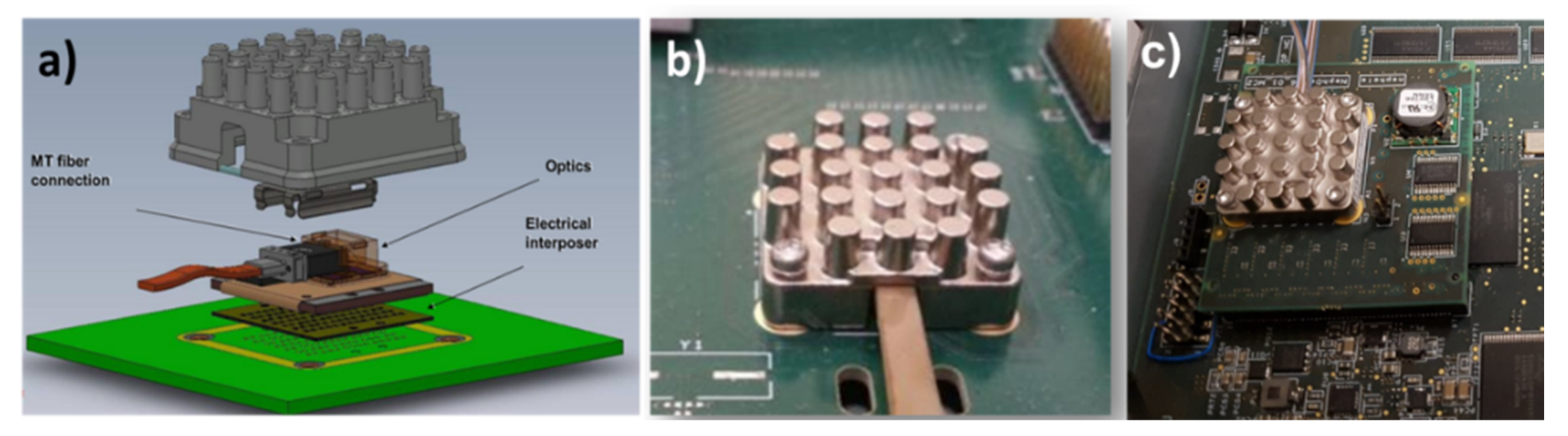
2. Midboard Optical Transceivers

The main advantage of midboard optical transceivers over more conventional card edge pluggable transceivers, such as the Quad Small Form-Factor Pluggable (QSFP) format [9], is that they can be placed close to the electronic signal source, such as a CPU, a Serial Attached SCSI expander switch chip or an Ethernet switch chip. This substantially reduces the electronic transmission line lengths between signal source and optical transceiver compared to edge pluggable transceivers. The resulting reduced signal integrity degradation enables energy savings at the port of the signal source by limiting or eliminating altogether the need for signal conditioning functions such as pre-emphasis or signal equalization. Furthermore, the reduced signal attenuation will allow the amplitude of the differential signal generated at the signal source to be reduced accordingly, and thus the power consumed by the signal port is also reduced. Depending on the type of signal source and the number of high-speed signal ports, this can result in a reduction in power consumption by as much as half in the signal source chip when the optical module is placed within 5 cm of the signal source chip [10].

2.1. Midboard Optical Transceivers

The choice of midboard optical transceiver on the controller boards for LightningValley, ThunderValley2 and Pegasus was the board-mounted optical assembly (BOA) from Finisar, supporting 12 bidirectional channels [11]. The BOAs used are protocol-independent and support SAS or Ethernet traffic at any line-rate up to 12 Gb/s, thus yielding a maximum bidirectional aggregate bandwidth of 144 Gb/s (12 × 12 Gb/s). Figure 2a shows the composition of the BOA module, which comprises an electrical interposer card, the optical transceiver multichip module, an optical receptacle supporting a 2 × 12 way MT ferrule connection and a heat sink. Figure 2b shows a photo of a BOA module mounted on a LightningValley controller card with a double layer polymer waveguide flexible ribbon attached. Figure 2c shows a photo of a BOA module mounted on an interchangeable mezzanine card in the Pegasus system.

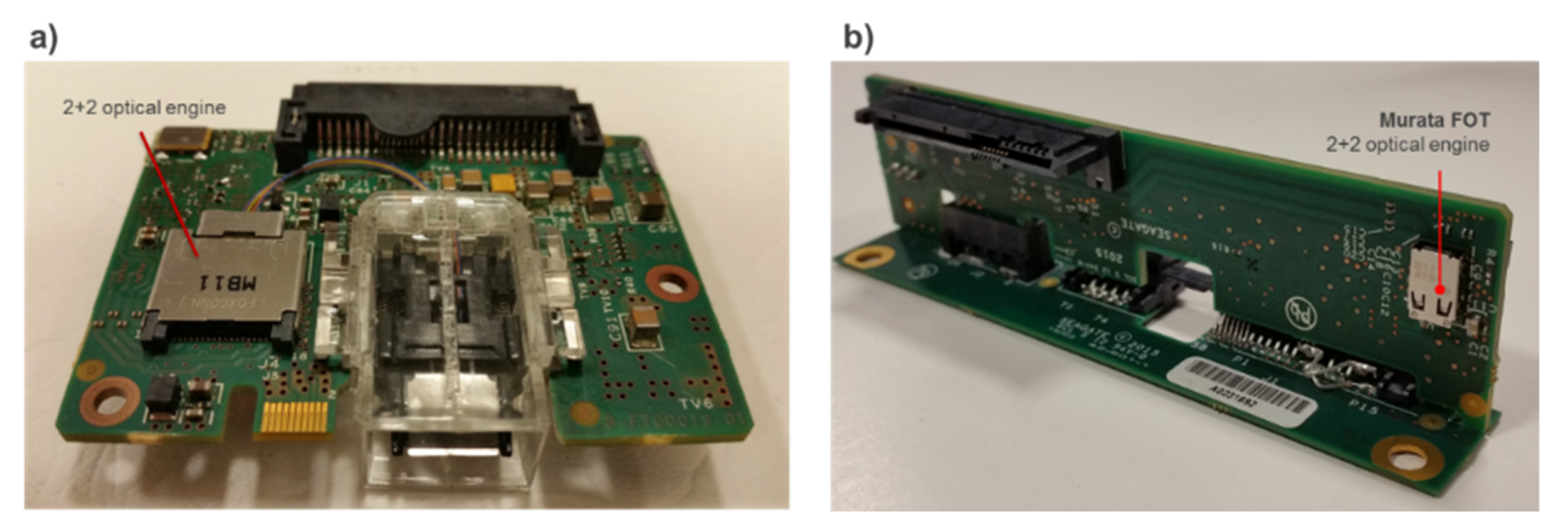
2.2. Low Port-Count Optical Transceivers

In distributed array systems where optical interconnects are required between arrays of end node devices such as hard disk drives or microservers, low port-count transceivers will be required, as shown in Figure 3.

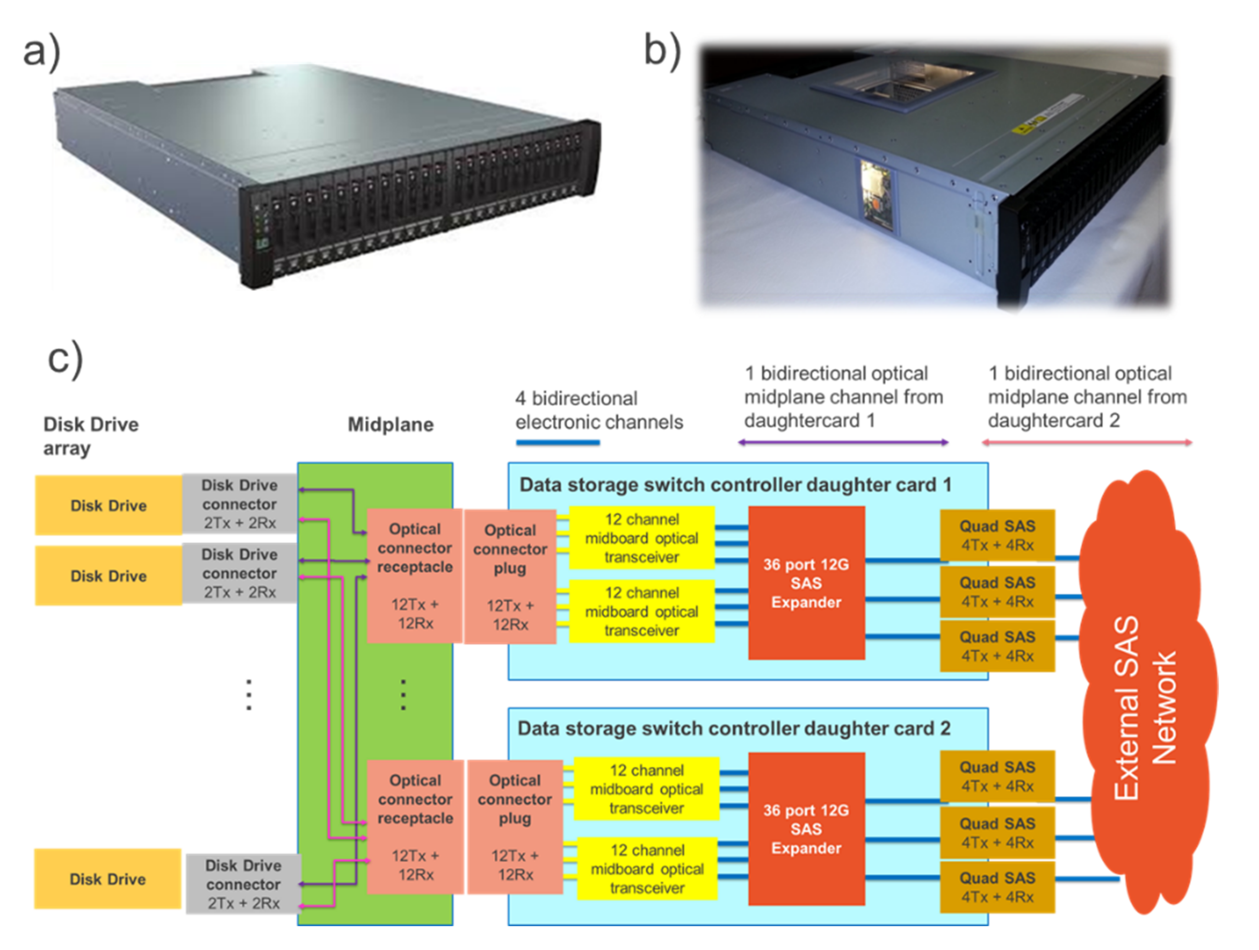
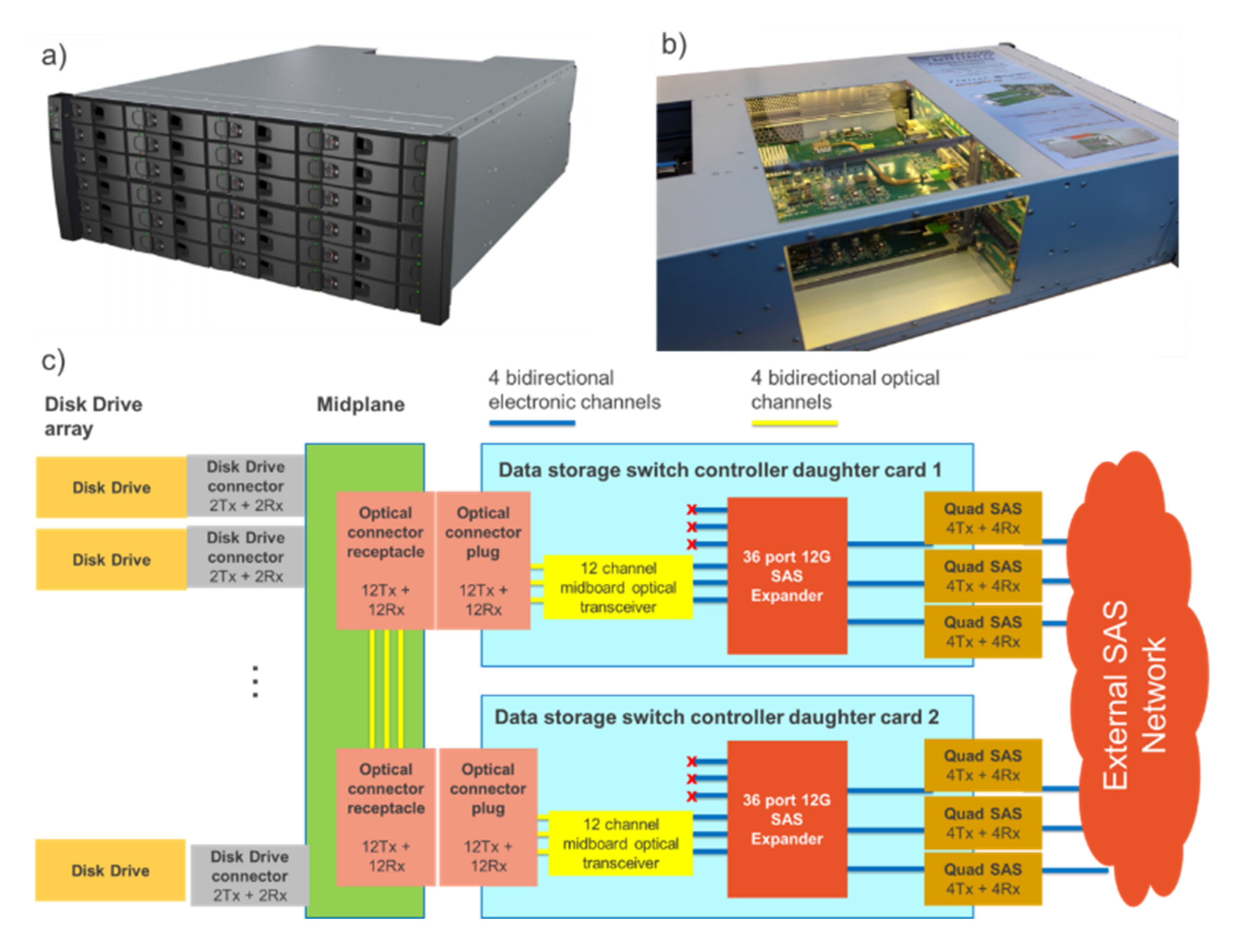
3. LightningValley—First-Generation Optically Enabled Data Center System

The LightningValley system (Figure 4b) was adapted from a 4U24 OneStor data storage array platform (Figure 4a). The system enclosure is 4U (177.8 mm) high and 19″ (482.6 mm) wide and supports an array of 24 3.5″ hard disk drives, which gives rise to the prefix 4U24. The LightningValley platform was modified to allow 12 bidirectional 12 Gb/s SAS channels to be conveyed optically from the expander chip of one controller daughtercard across an optical bridge on the midplane to the expander chip of the other controller daughtercard in the system (Figure 4c).
The LightningValley platform has been described in previous work [12,13,14]. In this section we focus on the optical interconnect technology and performance.

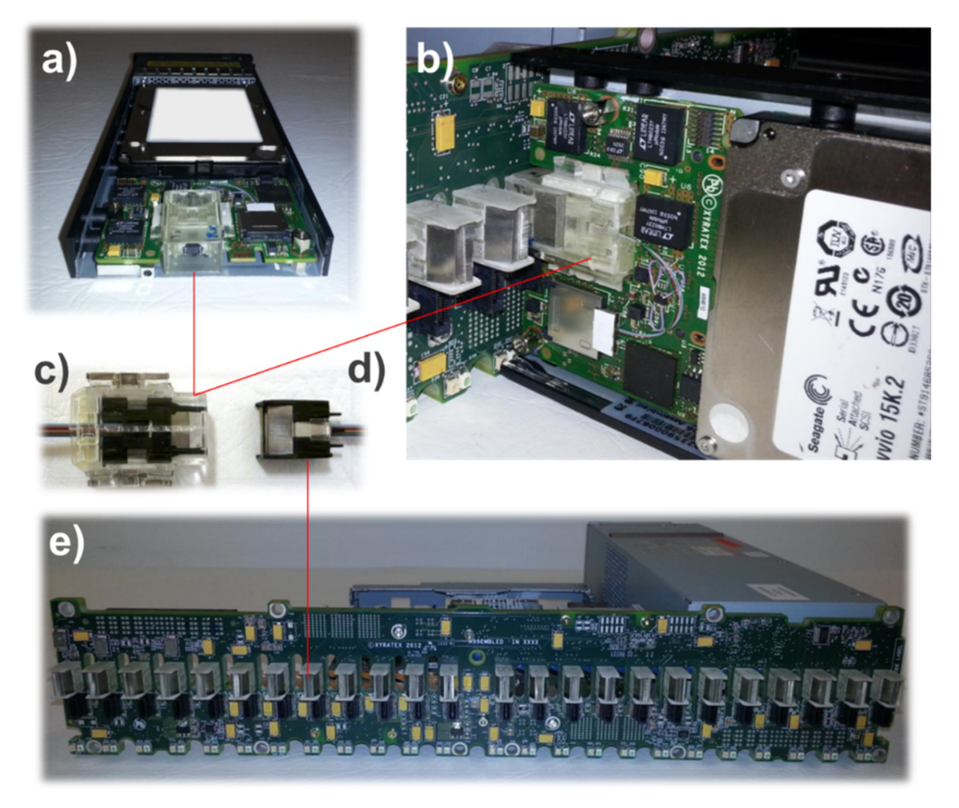
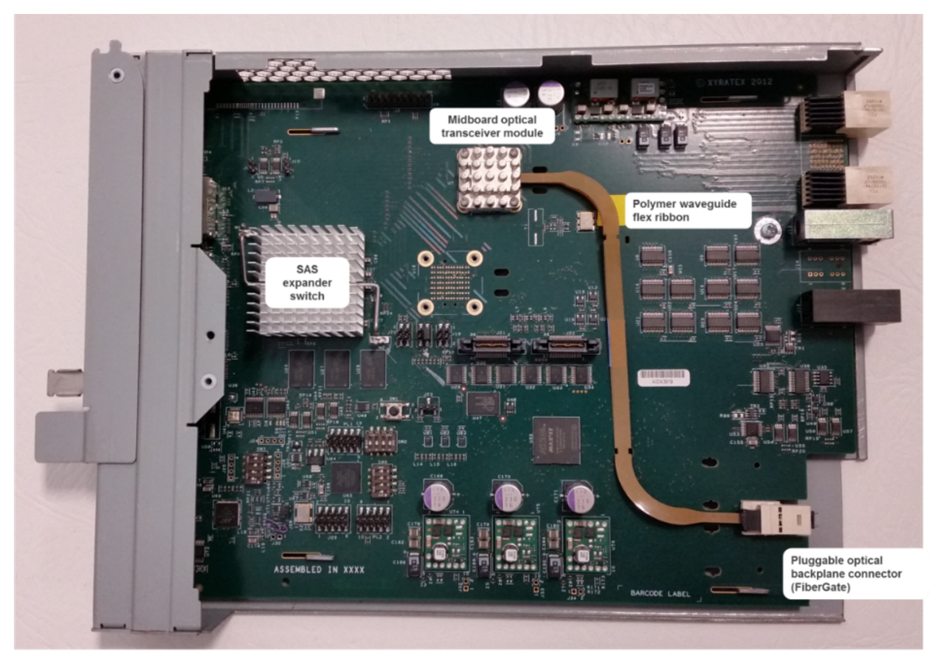
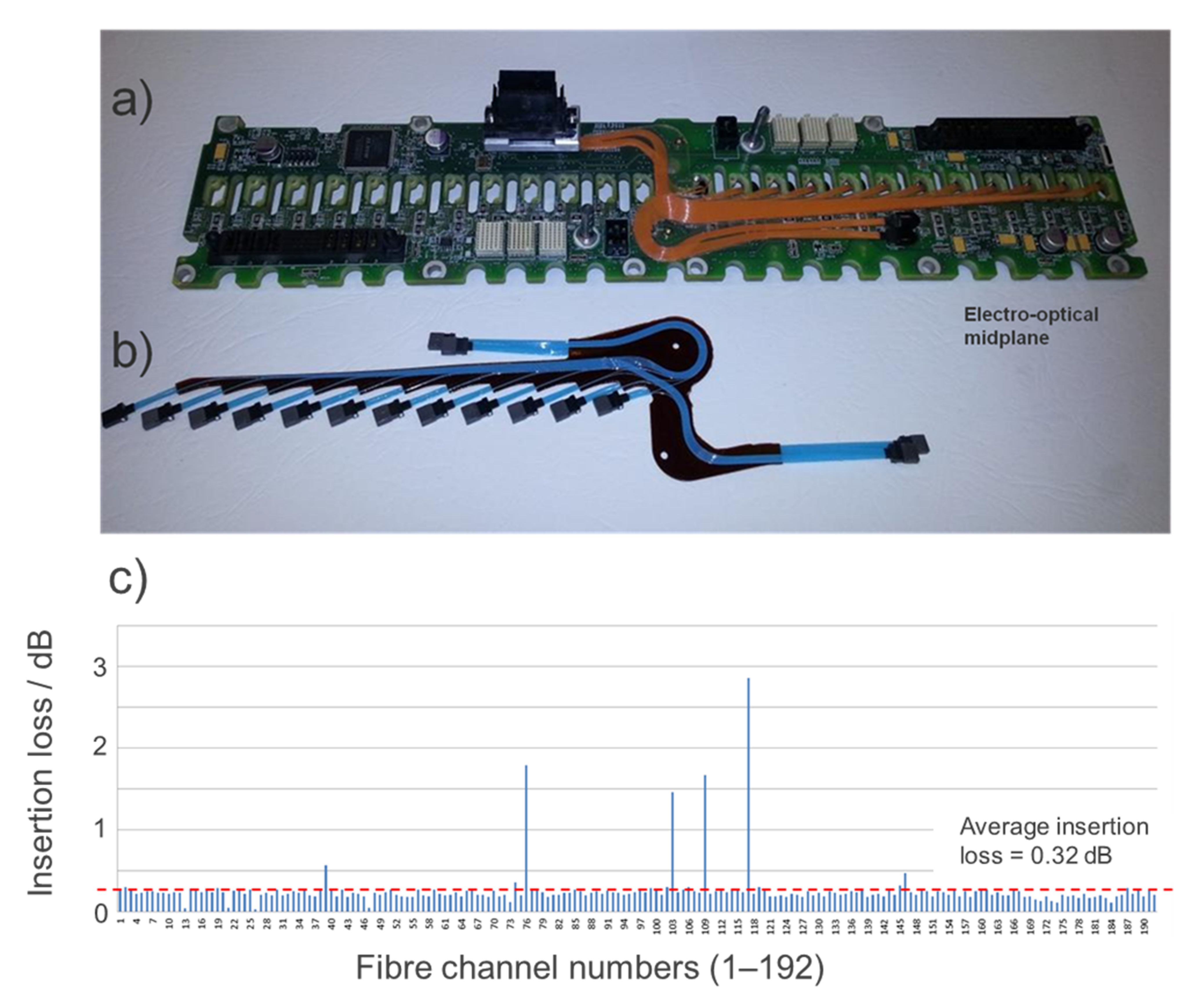
3.1. Optically Enabled Data Storage Switch Controller Daughtercards with Polymer Waveguide Interconnect

The controller daughtercards were modified such that 12 high-speed bidirectional electronic links from the SAS switch (expander) on the controller daughtercard to the midplane were converted to optical signals through the use of a Finisar BOA midboard optical transceiver module. The optical link on the controller daughtercards between the midboard optical transceiver modules and the optical midplane connector was conveyed across discrete, interchangeable dual-layer polymer optical ribbons. Figure 5 shows the optically modified LightningValley controller card with one BOA midboard optical transceiver mounted and a freestanding polymer waveguide flexible ribbon assembled providing the optical link between the midboard transceiver and the optical midplane connector. Each ribbon comprised two separate layers of polymer waveguides fabricated on an S-curved Kapton polyimide strip. Each layer contained 12 multimode polymer waveguides with a square cross-sectional profile of size 50 µm × 50 µm and separated by a center-to-center pitch of 250 µm, thus matching the horizontal interchannel separation used in MT ferrules. At each end of the ribbon cable, both layers of 12 waveguides were terminated into a bespoke ferrule, the interface of which was fully compliant with a single 2 × 12 MT interface.
The Swiss company Vario-optics manufactured the two types of dual-layer polymer optical waveguide flexible ribbon. The proprietary polymer acrylate material sets used to fabricate the waveguides were compatible with PCB manufacturing processes such as lamination, through-hole plating and reflow soldering and exhibited acceptable loss changes for long-term (2000 h) tests at elevated temperature (85 °C) and relative humidity (85%) as part of standard reliability tests, e.g., Telcordia GR-1221 [15].

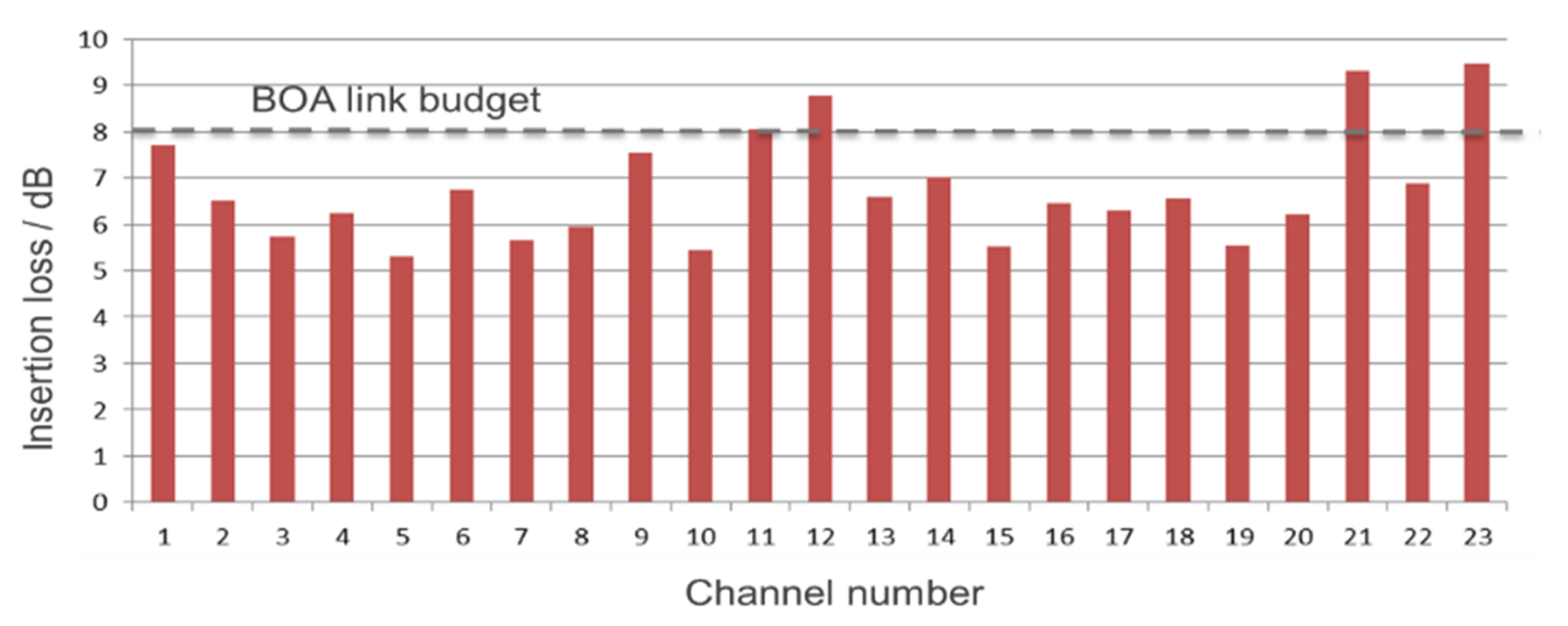
3.2. Polymer Interconnect Measurement Set-Up and Results

Insertion loss measurements were carried out on the polymer waveguide flex using an 850 nm VCSEL test light source. The reason for this is that all commercial midboard transceivers deployed in the reported systems use 850 nm VCSELs, which are high-volume commodity items. The 850 nm VCSEL test source was connected to a 5 m multimode graded-index optical fiber of category OM3 with a core size of 50 µm. The fiber was wound 10 times across a 50 mm diameter mandrel to produce a normalized modal launch condition. The full optical link path shown in Figure 5 is described as follows:
(a)
An optical signal generated in the BOA module on the first controller daughtercard couples into the 2 × 12 MT compliant ferrule of the first S-curved polymer waveguide flexible cable.
(b)
The signal propagates along the first S-curved flexible polymer waveguide cable.
(c)
At the card edge, the optical signal couples into the 2 × 12 MT compliant ferrule of the straight midplane polymer waveguide flex through the Huber + Suhner FiberGate connector.
(d)
The signal propagates along the midplane polymer waveguide flex from the first daughtercard location to the second controller daughtercard location.
(e)
The signal couples into the 2 × 12 MT compliant ferrule of the second S-curved flexible polymer waveguide cable through the FiberGate connector on the second controlled daughtercard.
(f)
The signal propagates along the second S-curved flexible polymer waveguide cable.
(g)
The signal couples into the optical interface of the BOA module on the second controller daughtercard.
The total transmitted power was measured across each of the 24 channels and compared to reference measurements in order to evaluate the insertion loss. The results are shown in Figure 6. The result for channel 24 was discarded as the channel was damaged. An average insertion loss of 6.76 dB was measured with a large standard deviation of 3.15 dB with 87% of waveguide links falling below the estimated BOA transceiver link budget of 8 dB. The size and variation in polymer waveguide insertion loss were too large to be considered for future variants of on-board interconnect, and so optical fiber flexplanes were adopted in the subsequent ThunderValley2 and Pegasus systems. It should be noted that since deployment in this early prototype, optical polymer formulations have continued to improve with polysiloxanes from Dow Corning [16] and Ormocer formulations such as “Sunconnect” by Nissan Chemicals [17].

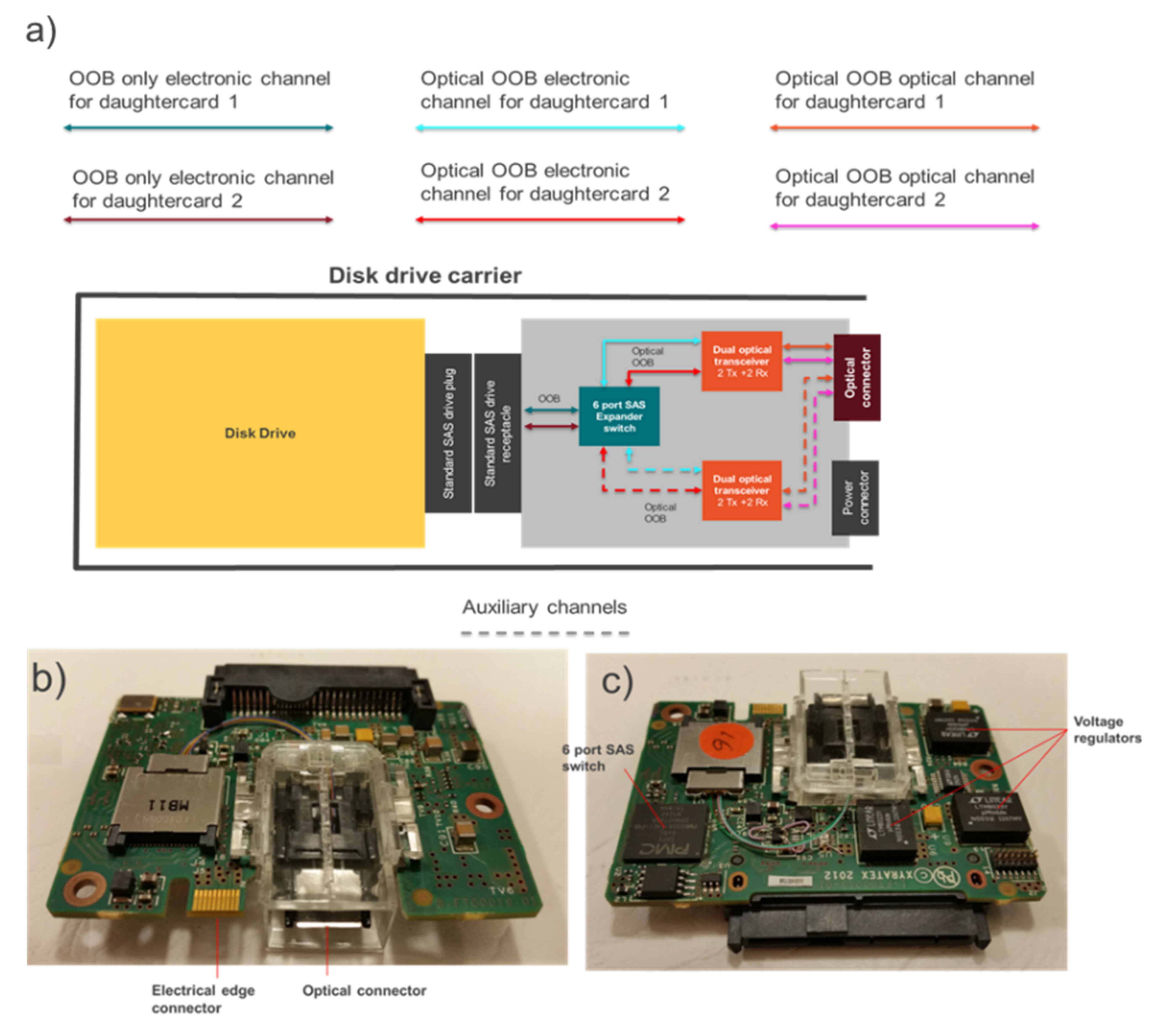
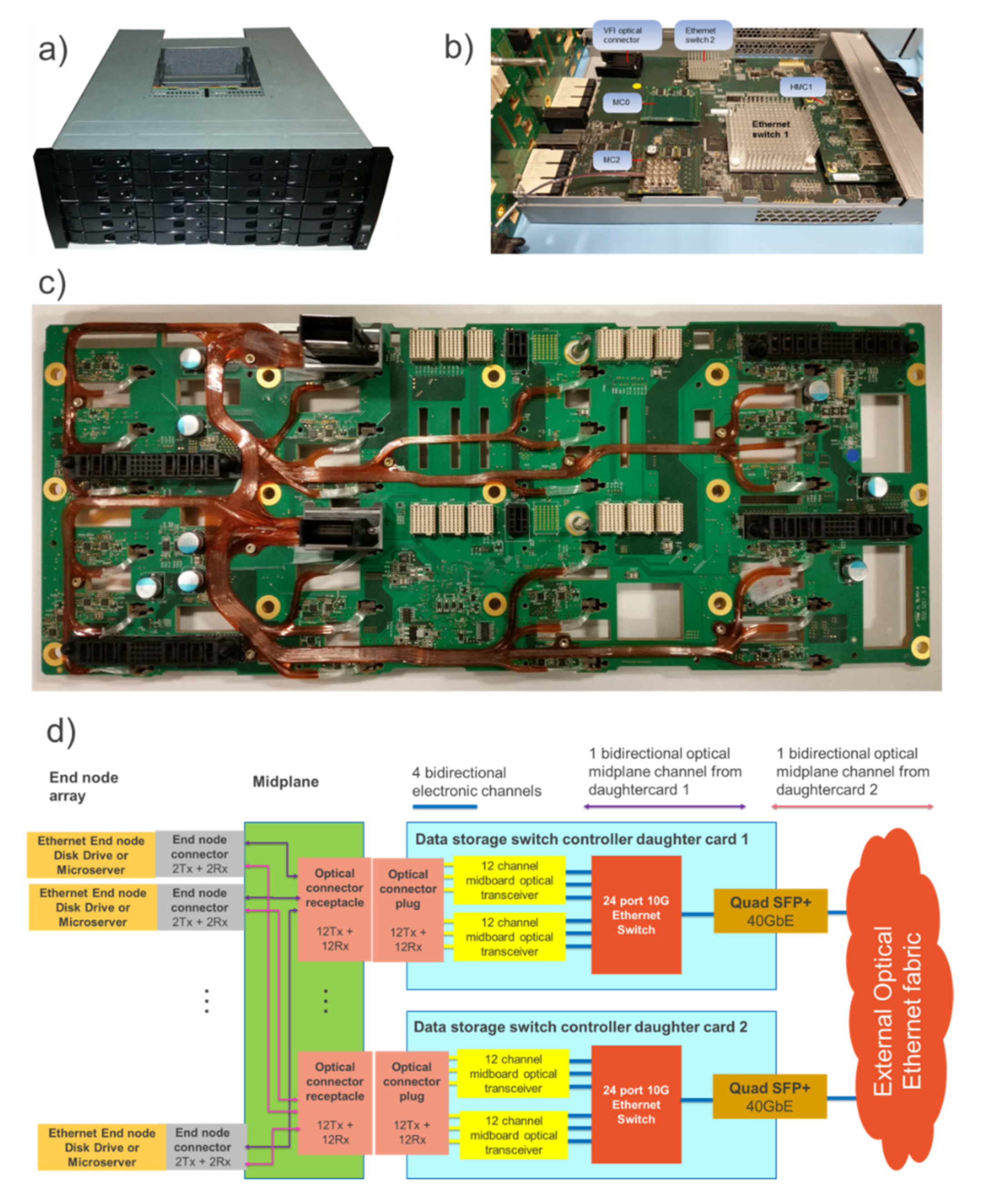
4. ThunderValley2—Second-Generation Optically Enabled Data Center System

The ThunderValley2 platform was adapted from an existing 2U (89 mm) high, 19″ (482.6 mm) wide OneStor system enclosure (Figure 7a) and included two optically enabled 12G SAS switch controller modules and an electro-optical midplane with a full aggregate bandwidth capacity of 2.3 Tb/s. Additionally, it provides the option to optically plug 24 conventional 2.5″ disk drives to the midplane (Figure 7b). The system architecture is shown in Figure 7c. As with the LightningValley system, the ThunderValley2 system supports two controller daughtercards, but it also allows 24 bidirectional 6 Gb/s SAS channels to be conveyed optically from the expander chip of each controller daughtercard to each of the 24 2.5″ disk drives across a fiber-optic flexplane attached to the midplane. An optical interface card is present on each disk drive to provide the opto-electronic signal conversion.
The ThunderValley2 platform was validated, with 6 Gb/s SAS data traffic successfully transmitted along the internal optical links, and has been described in previous work [5]. In this section we focus on the optical interconnect and interface technology and performance.

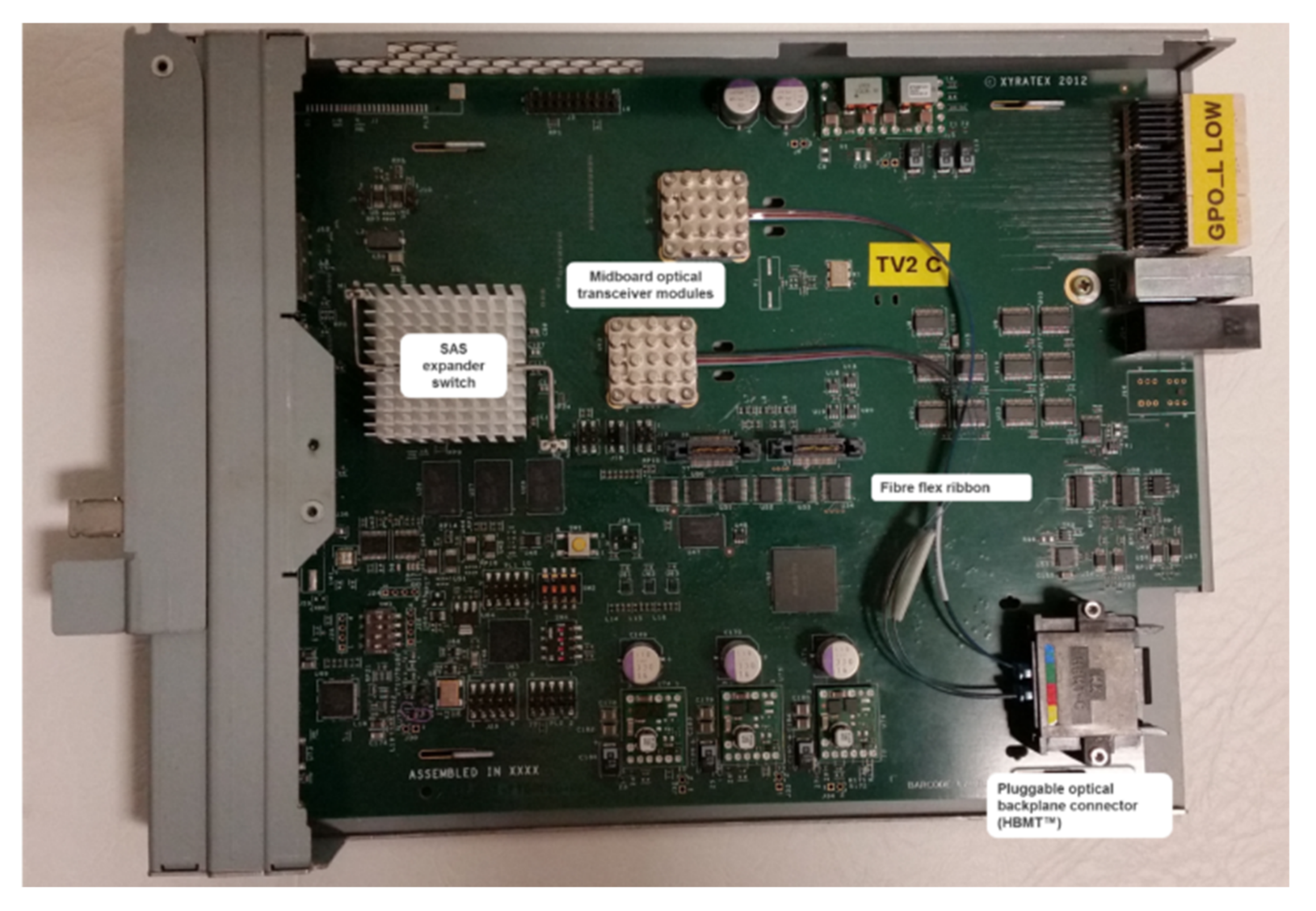
4.1. Optically Enabled Data Storage Switch Controller Daughtercards with Fiber Interconnect

The controller daughtercards were modified such that all 24 high-speed bidirectional electronic links from the SAS switch (expander) to the midplane were converted to optical signals through the use of two Finisar BOA midboard optical transceiver modules.
The optical links between the two midboard optical transceiver modules and two of the ferrule ports on the commercial Molex HBMT optical midplane connector were conveyed across discrete, interchangeable dual-layer multimode OM3 optical fiber ribbons (Figure 8).

4.2. Electro-Optical Midplane

The electro-optical midplane design was a modified version of the standard 2U midplane, in which all high-speed electrical transmission lines had been removed and provision made for a separate fiber flexible circuit laminate to be attached to the reduced electronic midplane PCB (Figure 9a). Consequently, the number of electronic layers in the midplane PCB was reduced by 55% and the open area available for airflow increased by 20%. The fiber flexplane comprised separate right-hand and left-hand sections (Figure 9b), each providing connectivity to 12 of the 24 slots.
The high-availability interconnect topology, in a passive dual-star configuration, required that each disk drive support two duplex data links situated on the midplane, one to each controller module. As a result, the midplane of the 24 SAS drive enclosure needed to support at least 48 duplex links (96 multimode OM3 fibers). To fully exploit the density advantages of optical interconnect, the midplane was designed for up to 96 duplex links (192 multimode OM3 fibers), thus providing for the future possibility of quad-lane drive interfaces (four independent duplex links per drive), for example through the deployment of PCIe drives, MultiLink SAS or Quad Ethernet interfaces. The midplane provided each drive with a separate, small, electrical connector for the purpose of supplying power and low-speed control signals with an optical midplane receptacle for high-speed SAS signals. The 192-fiber flexplane was terminated with four 2 × 12 MT ferrules on the controller side and twenty-four 1 × 12 MT ferrules on the drive side (of which only eight fibers per ferrule were populated). The flexplane was produced by TE Connectivity as part of the PhoxTroT project, and the optical link performance on all 192 fibers was measured using the same launch and measurement set-up described in Section 3.2 (Figure 9c). The optical link performance showed an average insertion loss of 0.32 dB with six fibers exhibiting abnormally high losses, due to partial damage during assembly. This shows that fiber, due to its maturity, is still far more suited for on-board interconnect than polymer waveguides and will be so for the foreseeable future.

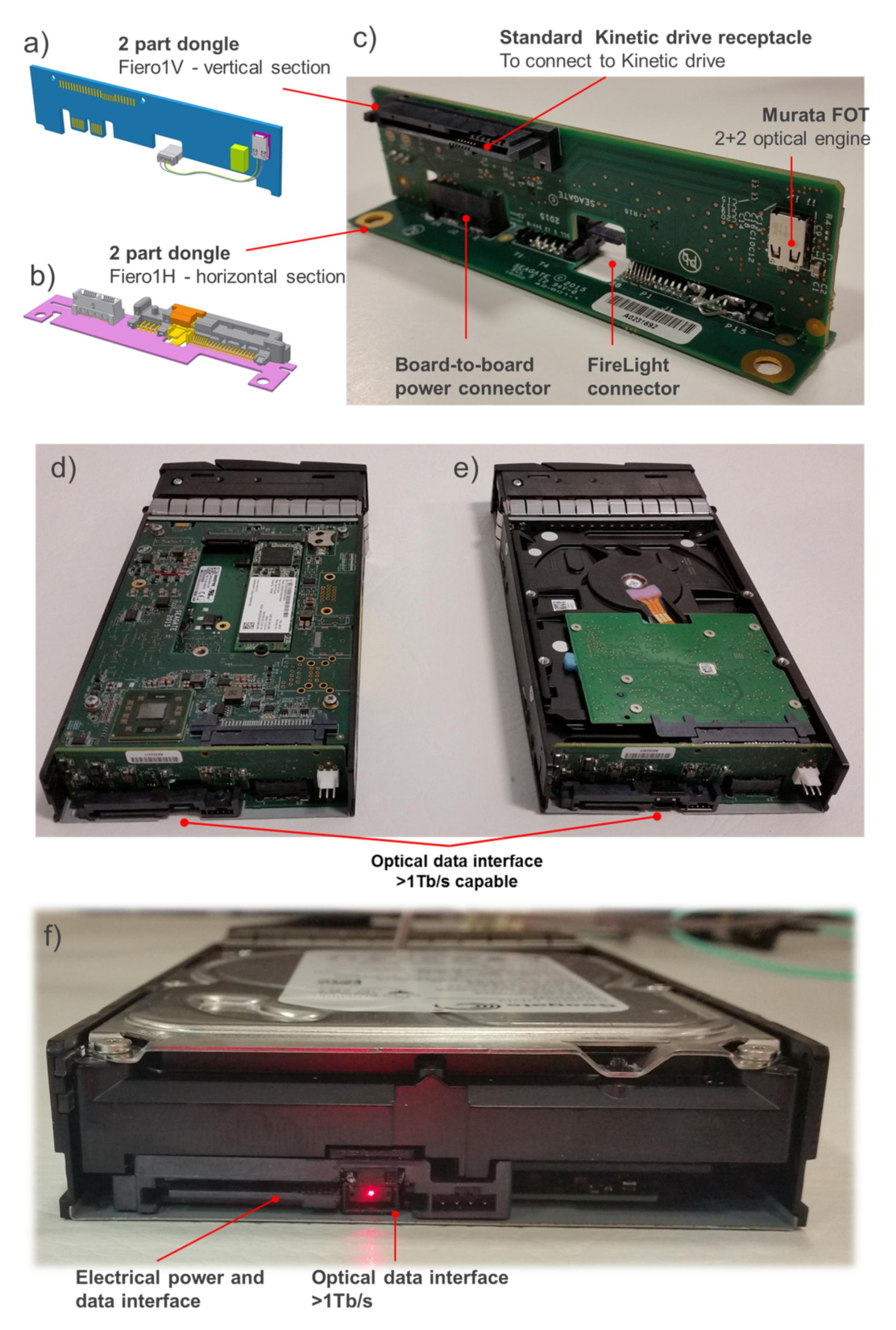
4.3. Optical Disk Drive Interface Card

A special interface card was designed to fit in the disk drive carrier and allow a standard 2.5″ hard disk drive to communicate and connect optically to the electro-optical midplane. Figure 10a shows the link topology of each optical interface card, which contained a proprietary “MorningStar” pluggable optical connector [18], two Avago McLink dual-channel board-mounted optical transceivers, a six-port SAS expander and an electrical connector compliant with conventional SAS/SATA disk drive interfaces. The hard disk drive supported 6 Gb/s SAS and maintained two bidirectional links to allow high availability connectivity. The SAS protocol allows optical communication between SAS devices only when a special mode, “optical OOB”, is supported.
The hard disk drive itself, however, did not support the optical OOB mode, and was restricted to electrical OOB, which inserts electrical idles of defined periods onto the high-speed link, making it unsuitable for direct connection to an optical transceiver. For this purpose, a six-port SAS expander was provided to serve as a bridge between the classical OOB of the disk drive and the optical OOB required to convey the signal through an optical transceiver. Although one dual-channel optical transceiver was sufficient to fully convey the two bidirectional links between the disk drive and the midplane, a second dual optical transceiver was added to serve as an auxiliary link, as shown with dashed lines in Figure 9a. In order to use this transceiver, the six-port SAS switch would simply need to be configured to convey the auxiliary links to the disk drive. The top and bottom sides of the optical interface card are shown in Figure 10b,c respectively.

4.4. Optical Disk Drive “MorningStar” Connector

The MT ferrule in turn was held within a Seagate proprietary “MorningStar” connector plug, which was attached to the edge of the interface card as shown in Figure 11. This parallel optical connector system comprises a plug that resides on the edge of the interface card (Figure 11a–c) and a receptacle that resides on the electro-optical midplane (Figure 11d,e). Guiding features included on the plug allow a receiving MT ferrule from the midplane receptacle to be connected precisely with a compliant MT ferrule in the plug section. The plug and receptacle enable a pluggable optical connection between the disk drive and the electro-optical midplane via the interface card.

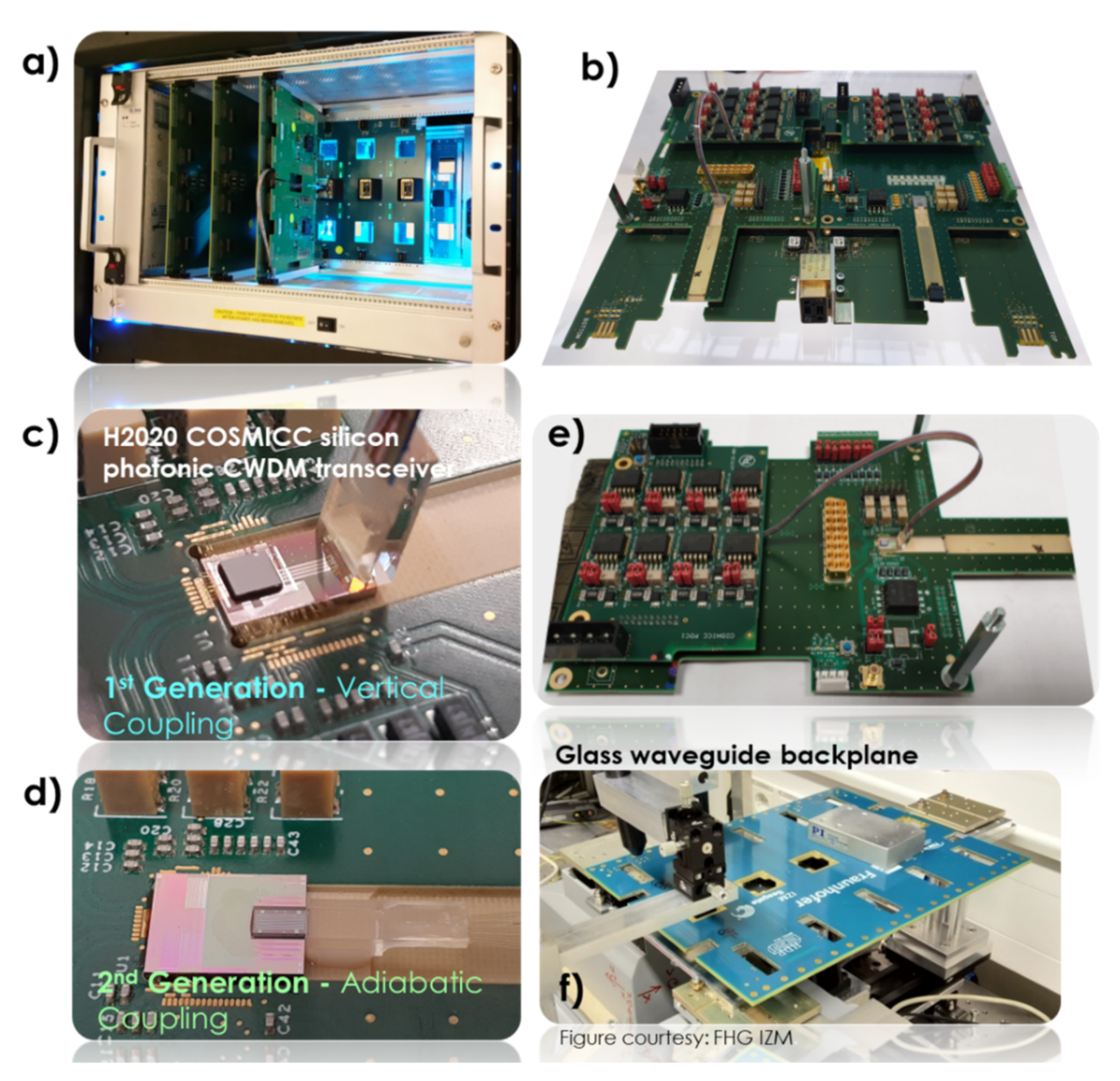
5. Pegasus—Third-Generation Optically Enabled Data Center System

The final-generation optically enabled data center system, Pegasus, comprised a converged switch, storage and compute platform. The switch controller modules and the compute and storage end nodes were optically interchangeable, independent entities within an object-oriented Ethernet framework, which was demonstrated on the Nephele project [19].
The Pegasus enclosure was based on a Seagate Technology 4U24 OneStor enclosure form factor (Figure 12a). The Pegasus interconnect topology, shown in Figure 12d, is based on a dual star configuration, whereby each end node (optically pluggable disk drive or microserver) supports two bidirectional data links on a proprietary electro-optical midplane (Figure 12c), one to each of two separate prototype Ethernet switch controller modules (Figure 12b).
The Pegasus platform has been described and characterized in previous work [8]. Here we focus on the optical interface technologies.

Optical End Node Connector Interface

To connect the storage or compute end nodes we developed a proprietary electro-optical connector [20] (Figure 13). The connector was based on an SFF-type hard disk drive connector, allowing it to be integrated onto a hard disk drive. This offers the potential for backward-compatible connectivity between current and future generations of disk drives. The connector retains power and high-speed electronic data interfaces; however, one section is reserved for high-density optical communication. This section includes a receptacle for a partially floating PrizmMT ferrule, which can accommodate up to 64 optical channels in a small space.
We designed a special two-part interface card (Figure 13c) to fit into a 3.5″ disk drive carrier in order to convert Ethernet data from optical signals from the midplane to electrical signals to the storage or compute end node. These comprised a vertical section holding a 2 + 2 Murata FOT optical transceiver (Figure 13a) and a horizontal section (Figure 13b) holding the electro-optical connector. Two varieties of optically interchangeable end node device were developed: (1) a storage device comprising a 3.5″ hard disk drive with an Ethernet communications interface (Figure 13d) and (2) a compute device, which comprised a microserver platform with an Ethernet communications interface (Figure 13e). Both included the optical interface card and electro-optical connector allowing them to be optically pluggable and interchangeable.

6. Aurora—Hyperscale Integrated Optical and Photonics Ecosystem Demonstrator Platform

The FP7 PhoxTroT, H2020 Nephele and H2020 COSMICC projects developed a test and measurement platform, named “Aurora”, that enabled the systematic characterization of optical transceivers, board-to-board optical connectors and both embedded and passive optical circuit boards, as shown in Figure 14 [21,22].
The cross-project “Aurora” platform is designed to hold different types of advanced optical interconnect technologies including embedded and discrete polymer and glass waveguide circuits, optical PCB connectors and transceiver and switch technologies including advanced silicon photonics devices.
Aurora comprised a test enclosure with interlocking and interchangeable mezzanine electro-optical test boards, electro-optical daughterboards and electro-optical backplanes. This allows the characterization of different optical components with different technical maturity levels either alone or in combination with other technologies. The initial work was carried out during the PhoxTroT project (which concluded in May 2017) [24]. The H2020 Nephele [25] and H2020 COSMICC [26] projects further developed the Aurora universal test platform, building it into an open-source test board design portfolio, which was widely disseminated. Organizations or consortia can use Aurora to test diverse integrated optical and photonic interconnect technologies on a common platform. Researchers only need to focus on the design of small simple test cards using the common design form factors, thus giving significant time and cost savings. The need to design a new evaluation platform from scratch is avoided, allowing researchers to make more technology iterations and accelerate the movement of the target technology through the TRL levels. The test boards can be used on their own or connected to appropriate communication platforms.
An international standard (IEC 62150-6 Ed1—Basic Test and Measurements, Universal Test Cards for Test and Measurement of Micro Board Photonic Devices) will be published in 2022. This standard defines the generic electro-optic mezzanine board for the test and measurement of micro-optical and microphotonic devices, including a wide diversity of photonic integrated circuit (PIC) technologies spanning technologies from transceivers, switches, sensors, neuromorphic networks and LiDAR to quantum integrated circuits. In addition to European research and development projects FP7 PhoxTroT [27], H2020 Nephele [28] and H2020 COSMICC [6], the Aurora platform with new variants of these mezzanine boards has formed the basis of the United States of America High Density User Packaging Group (HDPuG) Opto-electronics project, which culminated in a comprehensive round-robin between multinational organizations including Cisco, Corning, Nokia, Seagate, Fujitsu, Huber + Suhner, Fraunhofer IZM, R&M, Samtec and TTM Technologies.

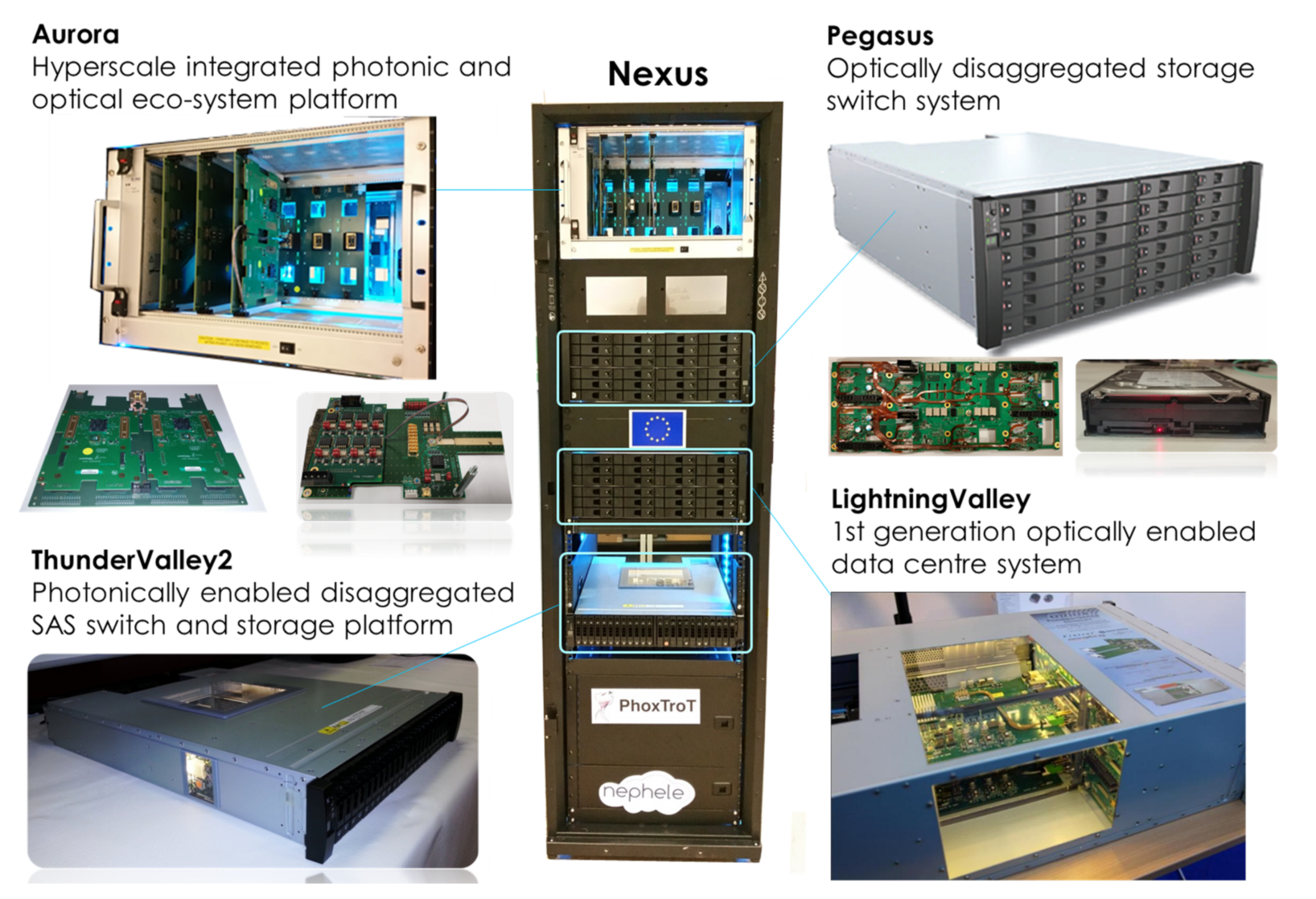
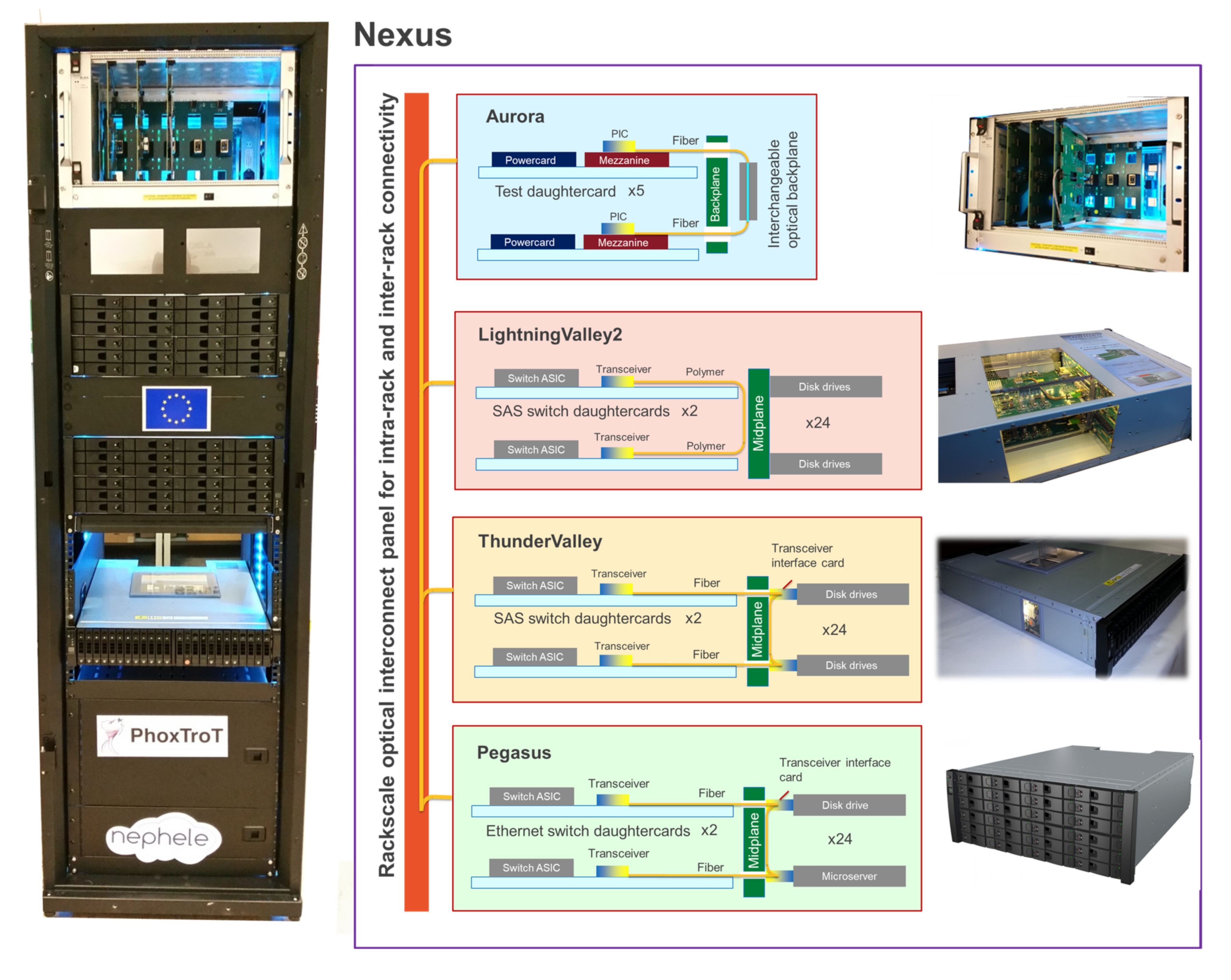
7. Nexus—Fully Converged Rack-Scale Data Center Test Platform

A converged rack-scale platform, “Nexus”, was developed based on the FP7 PhoxTroT project to support the different fully functional optically enabled data storage and switch platforms and provide an interconnection matrix, which would allow them to be characterized and validated for different lengths and configurations of optical interconnects. In addition to the functional optically enabled systems, there is provision for the universal optical interconnect platform, “Aurora” described in the previous section.
As part of the Nexus platform, the Aurora platform allows for advanced, low technical maturity passive and active interconnect technologies to be directly validated with the optically enabled optical data center demonstrators LightningValley2, ThunderValley and Pegasus in the same rack (Figure 15).

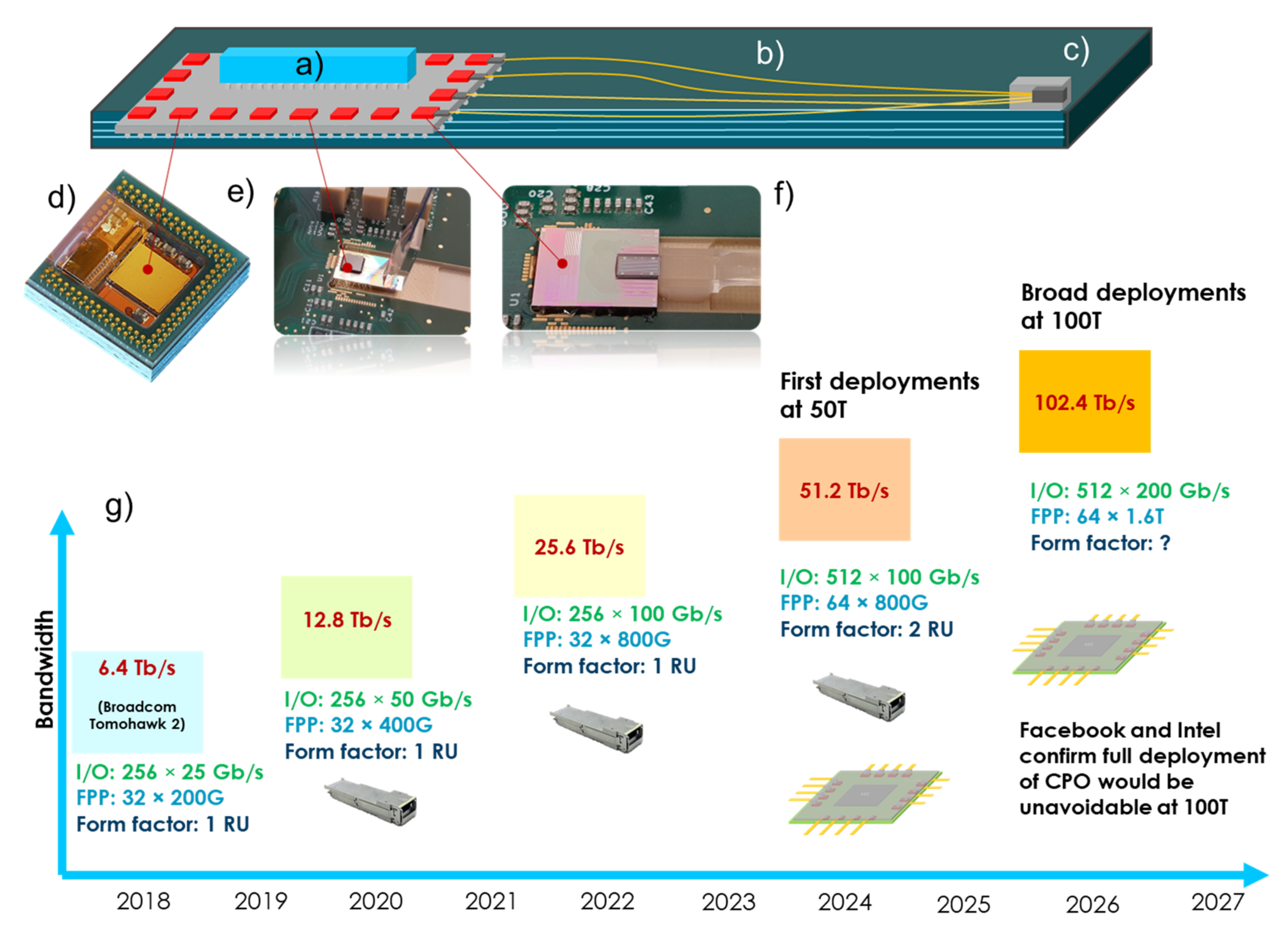
8. Copackaged Optical Assembly—The Ultimate Migration of System-Level Optical Interconnect

Hyperscale data centers are very large data centers typically comprising at least hundreds of thousands of servers and associated storage and networking capacity, and they are run by major internet content providers, such as Google, Microsoft, Amazon and Alibaba, to provide “cloud” services. By 2021 hyperscale data centers have become the dominant form of data center in the world, overtaking private and enterprise data centers, with most organizations outsourcing their data storage requirements to these highly secure facilities with guaranteed quality of service.
Fiber-optic infrastructure is already well established in hyperscale data centers to connect together thousands of racks filled with servers, storage arrays and switch enclosures. External fiber-optic connections are made to optical transceivers, which are plugged onto the “face-plate” of such enclosures, hence the term face-plate pluggable (FPP) modules; however, the exponential increase in data consumption is pushing the bandwidth of data center switch enclosures to the point where there is now not enough space on the face-plate for the transceivers to meet this demand. As shown in Figure 16g, data center switch ASICs of 51 Tbps are expected to be introduced by 2024, and those of 100 Tbps are expected before 2027, which represent substantially higher bandwidths than the bisection bandwidths reported in the demonstration platforms in this paper. There are now massive efforts underway to move optical transceiver cores or “chiplets” into the switch ASIC package itself, in so-called copackaged optical (CPO) assemblies as shown in Figure 16a [29].
As reported in this paper, migration of optical interconnect to the system, board and chip level will be required to substantially mitigate the communications bottlenecks resulting from the increase in both per-lane bandwidth and internal interconnect link lengths. At the board level, this migration will see the development of electro-optical circuit boards comprising detachable fiber shuffles, but in the future, embedded polymer or glass waveguides [30] may play an increasing role if the propagation losses can be reduced to be comparable to those of fiber.
While front-pluggable and midboard transceivers are evolving, at the chip level, photonic integrated circuit technology (e.g., silicon photonics) has opened the door to the deployment of microtransceiver chiplets (Figure 16d–f) in CPO modules. Front-panel, midplane, backplane and midboard passive optical connectors will be an essential part of this ecosystem connecting system to board to chip.
In this paper we have reported on the first generation of midboard transceivers introduced in 2012; however, by 2020 these fixed modules had become largely obsolete due to lack of field replaceability. The second generation of midboard transceivers specified by the Consortium for On-Board Optics (COBO) are pluggable onto the middle of the board [34]; however, as they are still in separate modules, they would take up a lot of valuable board area. Therefore, it is expected that in such switch enclosures midboard transceivers will be bypassed altogether with a combination of FPPs and CPO modules used to accommodate the huge data center switch bandwidths.
Currently, a 12.8 Tbps switch can be accommodated by 32 400 G face-plate pluggable (FPP) transceiver modules, which fill the face-plate area of a standard 1 RU high enclosure. In order to accommodate a 51.2 Tbps switch with four times the I/O bandwidth of a 12.8 Tbps switch, it is envisaged that sixteen 3.2 Tbps CPO engines [35] will be required with potentially four times the number of fibers at the front face-plate. In addition, most CPO solutions will use an external light source (ELS) to provide the source of continuous-wave light to the modulators in the chiplets, and this ELS module will preferably also be a pluggable module on the face-plate, which will further reduce the available space on the face-plate.
The media by which optical signals are conveyed between the on-board CPO module and the passive optical connectors on the front face-plate will at first be fiber due to its maturity and availability. In applications where the number of fibers becomes prohibitive, sophisticated fiber management solutions will be introduced, such as under-board fiber shuffles. The media on the CPO module itself to provide the possibly hundreds of optical connections between the chiplets and the main board outside the CPO module will also be fiber-based in the short term; however, other media such as polymer waveguides [36] and planar glass waveguides [37,38] have also been investigated.

9. Conclusions and Further Work

We have reported on the evolution of system embedded optical interconnect technologies in optically enabled sub-TOR data center systems. The architectures of three generations of optically enabled data storage, switch and compute platforms have been described; the first two generations demonstrated partially and fully optically enabled data storage and switch capability based on the SAS protocol while the final generation demonstrated a fully optically disaggregated, object-oriented system based on Ethernet and the Seagate OpenStorage protocol. In addition, we have described and comparatively characterized electro-midplanes based on multimode polymer and multimode fiber flexible circuits, described optical interface cards allowing standard edge storage and compute devices to be connected into an optical topology and introduced a proprietary electro-optical connector for object-oriented end nodes.
Looking ahead to the continual evolution of optical interconnects, which are expected to mature as a prerequisite to complete disaggregation of compute, memory and storage, the Aurora and Nexus platforms provide mechanisms by which third-party vendors providing optical hardware can be assessed for performance and compared against competing offerings.

Author Contributions

Conceptualization, R.P., L.O., S.A.S. and A.R.; methodology, R.P. and K.W.; validation, R.P., K.W., A.M. and V.D.; investigation, R.P., K.W., A.M. and V.D.; writing—original draft preparation, R.P. and L.O.; writing—review and editing, A.R., A.J., K.G., S.A.S. and L.O.; visualization, A.R., A.J., K.G. and R.P.; project administration, R.P. All authors have read and agreed to the published version of the manuscript.

Funding

This research was funded by the EU FP7 project “PhoxTrot”, for which it has received funding from the European Union Seventh Framework Programme (FP7/2007–2013) under grant agreement No. 318240, the Horizon2020 Nephele project (Grant No. 645212), the Horizon2020 COSMICC project (Grant No. 688516).

Institutional Review Board Statement

Not applicable.

Informed Consent Statement

Not applicable.

Data Availability Statement

Not applicable.

Conflicts of Interest

The authors declare no conflict of interest.

References

  1. Mahajan, R.; Li, X.; Fryman, J.; Zhang, Z.; Nekkanty, S.; Tadayon, P.; Jaussi, J.; Shumarayev, S.; Agrawal, A.; Jadhav, S.; et al. Co-Packaged Photonics for High Performance Computing: Status, Challenges and Opportunities. J. Light. Technol. 2021, 40, e3104725. [Google Scholar] [CrossRef]
  2. Fathololoumi, S.; Nguyen, K.; Mahalingam, H.; Sakib, M.; Li, Z.; Seibert, C.; Montazeri, M.; Chen, J.; Doylend, J.K.; Jayatilleka, H.; et al. 1.6 Tbps Silicon Photonics Integrated Circuit for Co-Packaged Optical-IO Switch Applications. In Proceedings of the Optical Fiber Communication Conference (OFC), San Diego, CA, USA, 13 March 2020; p. T3H.1. [Google Scholar]
  3. Liao, L.; Fathololoumi, S.; Hui, D. High Density Silicon Photonic Integrated Circuits and Photonic Engine for Optical Co-packaged Ethernet Switch. In Proceedings of the 2020 European Conference on Optical Communications (ECOC), Brussels, Belgium, 20–24 September 2020; pp. 1–4. [Google Scholar] [CrossRef]
  4. Schmidtke, K.; Flens, F.; Worrall, A.; Pitwon, R.; Betschon, F.; Lamprecht, T.; Kraehenbuehl, R. 960 Gb/s optical backplane using embedded polymer waveguides and demonstration in a 12G SAS storage array. In Proceedings of the 2013 Optical Interconnects Conference, Santa Fe, NM, USA, 5–8 May 2013; pp. 29–30. [Google Scholar] [CrossRef]
  5. Pitwon, R.; Worrall, A.; Stevens, P.; Miller, A.; Wang, K.; Schmidtke, K. Demonstration of fully enabled data center subsystem with embedded optical interconnect. In Proceedings of the Optical Interconnects Xiv, San Francisco, CA, USA, 8 March 2014; Volume 8991, p. 899110. [Google Scholar] [CrossRef]
  6. Pitwon, R.C.; Immonen, M.; Schroeder, H.; Neitz, M.; Wang, K. Universal test system for system embedded optical interconnect. In Proceedings of the SPIE—The International Society for Optical Engineering, San Francisco, CA, USA, 22 February 2018; Volume 10538, p. 1053804. [Google Scholar]
  7. Pitwon, R.; O’Faolain, L. Modular test system for high-speed silicon photonics transceivers. In Proceedings of the SPIE—The International Society for Optical Engineering, San Francisco, CA, USA, 4 March 2019; Volume 10924, p. 109240I. [Google Scholar]
  8. Pitwon, R.; Wang, K.; Worrall, A. Converged photonic data storage and switch platform for exascale disaggregated data centers. In Proceedings of the SPIE—The International Society for Optical Engineering, San Francisco, CA, USA, 20 February 2017; Volume 10109. [Google Scholar] [CrossRef]
  9. Ghiasi, A.; Nowell, M.; Sommers, S. QSFP-DD/QSFP-DD800/QSFP112 Hardware Specification for QSFP DOUBLE DENSITY 8X AND QSFP 4X PLUGGABLE TRANSCEIVERS. QSFD-DD MSARevision 6.0128 May 2021. Available online: http://www.qsfp-dd.com/wp-content/uploads/2021/05/QSFP-DD-Hardware-Rev6.01.pdf (accessed on 15 October 2021).
  10. Schmidtke, K.; Flens, F. Trends and Future Directions in Optical Interconnects for Datacenter and Computer Applications. In Proceedings of the Optical Fiber Communication Conference Postdeadline Papers; The Optical Society: San Diego, CA, USA, 2010; p. OTuP4. [Google Scholar]
  11. Schmidtke, K.E.; Flens, F.; Mahgarefteh, D. Taking Optics to the Chip: From Board-mounted Optical Assemblies to Chip-level Optical Interconnects. In Proceedings of the Optical Fiber Communication Conference, San Francisco, CA, USA, 9 March 2014; pp. 1–3. [Google Scholar]
  12. Maniotis, P.; Terzenidis, N.; Siokis, A.; Christodoulopoulos, K.; Varvarigos, E.; Immonen, M.; Yan, H.J.; Zhu, L.X.; Hasharoni, K.; Pitwon, R.; et al. Application-Oriented On-Board Optical Technologies for HPCs. J. Light. Technol. 2017, 35, 3197–3213. [Google Scholar] [CrossRef]
  13. Schmidtke, K.; Flens, F.; Worrall, A.; Pitwon, R.; Betschon, F.; Lamprecht, T.; Krahenbuhl, R. 960 Gb/s Optical Backplane Ecosystem Using Embedded Polymer Waveguides and Demonstration in a 12G SAS Storage Array. J. Light. Technol. 2013, 31, 3970–3975. [Google Scholar] [CrossRef]
  14. Flens, F. Fiber Optics Packaging. In Proceeding of the Optical Fiber Communication Conference, Los Angeles, CA, USA, 22–26 March 2015; Paper Th1G.4; Optica Publishing Group: Washington, DC, USA, 2015. [Google Scholar]
  15. Telcordia. Generic Reliability Assurance Requirements for Passive Optical Components. 2010. Available online: https://telecom-info.njdepot.ericsson.net/ido/AUX/GR_1221_TOC.i02.pdf (accessed on 15 October 2021).
  16. Kruse, K.; Middlebrook, C. Laser-direct writing of single mode and multi-mode polymer step index waveguide structures for optical backplanes and interconnection assemblies. Photonics Nanostruct.-Fundam. Appl. 2015, 13, 66–73. [Google Scholar] [CrossRef]
  17. Nawata, H.; Oshima, J.; Kashino, T. Organic-inorganic hybrid material SUNCONNECT(R) for photonic integrated circuit. In Optical Interconnects XVIII; International Society for Optics and Photonics: Bellingham, WA, USA, 2018; Volume 10538, pp. 70–78. [Google Scholar] [CrossRef]
  18. Pitwon, R.C.A.; Brusberg, L.; Schroder, H.; Whalley, S.; Wang, K.; Miller, A.; Stevens, P.; Worrall, A.; Messina, A.; Cole, A. Pluggable Electro-Optical Circuit Board Interconnect Based on Embedded Graded-Index Planar Glass Waveguides. J. Light. Technol. 2014, 33, 741–754. [Google Scholar] [CrossRef]
  19. Tokas, K.; Spatharakis, C.; Patronas, I.; Bakopoulos, P.; Landi, G.; Christodoulopoulos, K.; Capitani, M.; Kyriakos, A.; Aziz, M.; Pitwon, R.; et al. Real Time Demonstration of an End-to-End Optical Datacenter Network with Dynamic Bandwidth Allocation. In Proceedings of the 44th European Conference on Optical Communication-ECOC, Rome, Italy, 23–27 September 2018; pp. 1–3. [Google Scholar]
  20. Pitwon, R.; Miller, A. Optical Connectors. U.S. Patent 10,732,360, 4 August 2020. [Google Scholar]
  21. Kurata, K.; Pitwon, R. Short reach, low cost silicon photonic micro-transceivers for embedded and co-packaged system integration. In Proceedings of the Optical Interconnects XX, San Francisco, CA, USA, 1–6 February 2020. [Google Scholar]
  22. Pitwon, R.; O’Faolain, L.; Kurata, K.; Lee, B.; Ninomyia, T. Hyperscale Integrated Optical and Photonic Interconnect Platform. In Proceedings of the 2020 IEEE Photonics Conference (IPC), Vancouver, BC, Canada, 28 September–1 October 2020. [Google Scholar] [CrossRef]
  23. Pitwon, R. System embedded photonic interconnect for mega-data centre environments. In Proceedings of the 2016 IEEE CPMT Symposium Japan (ICSJ), Kyoto, Japan, 7–9 November 2016; pp. 87–90. [Google Scholar] [CrossRef] [Green Version]
  24. Fraunhofer, I.Z.M. Press Release PhoxTroT: Optical Interconnect Technologies Revolutionized Data Centers and HPC Systems. Available online: http://www.phoxtrot.eu/press-release/ (accessed on 23 December 2017).
  25. National Technical University of Athens. Nephele Project. Available online: http://www.nepheleproject.eu (accessed on 8 December 2015).
  26. CEA-LETI. Horizon 2020 COSMICC Project. Available online: http://www.h2020-cosmicc.com (accessed on 15 October 2021).
  27. Hakansson, A.; Tekin, T.; Brusberg, L.; Pleros, N.; Vyrsokinos, C.; Apostolopoulos, D.; Pitwon, R.; Miller, A.; Wang, K.; Tulli, D.; et al. PhoxTroT—A European initiative toward low cost and low power photonic interconnects for data centres. In Proceedings of the 2015 17th International Conference on Transparent Optical Networks, Budapest, Hungary, 5–9 July 2015; pp. 1–5. [Google Scholar]
  28. Bakopoulos, P.; Christodoulopoulos, K.; Landi, G.; Aziz, M.; Zahavi, E.; Gallico, D.; Pitwon, R.; Tokas, K.; Patronas, I.; Capitani, M.; et al. NEPHELE: An End-to-End Scalable and Dynamically Reconfigurable Optical Architecture for Application-Aware SDN Cloud Data Centers. IEEE Commun. Mag. 2018, 56, 178–188. [Google Scholar] [CrossRef]
  29. Stone, R.; Chen, R.; Rahn, J.; Venkataraman, S.; Wang, X.; Schmidtke, K.; Stewart, J. Co-packaged Optics for Data Center Switching. In Proceedings of the 2020 European Conference on Optical Communications (ECOC), Brussels, Belgium, 6–10 December 2020; pp. 1–3. [Google Scholar] [CrossRef]
  30. Pitwon, R.; Yamauchi, A.; Brusberg, L.; Wang, K.; Ishigure, T.; Neitz, M.; Worrall, A. Planar polymer and glass graded index waveguides for data center applications. Opt. Interconnects XVI 2016, 9753, 97530. [Google Scholar] [CrossRef]
  31. Kurata, K.; Hagihara, Y.; Kurihara, M.; Yashiki, K.; Kinoshita, K.; Shiba, K.; Kuwata, M.; Muto, T.; Kobayashi, S.; Baba, N.; et al. Short reach, high temperature operation and high reliability silicon photonic micro-transceivers for embedded and co-packaged system integration. In Optical Interconnects XXI; SPIE: Bellingham, WA, USA, 2021; Volume 11692, p. 1169204. [Google Scholar]
  32. Kurata, K.; Giorgi, L.; Cavaliere, F.; O’Faolain, L.; Schulz, S.A.; Nishiyama, K.; Hagihara, Y.; Yashiki, K.; Muto, T.; Kobayashi, S.; et al. Silicon Photonic Micro-Transceivers for Beyond 5G Environments. Appl. Sci. 2021, 22, 10955. [Google Scholar] [CrossRef]
  33. Olivier, S.; Sciancalepore, C.; Hassan, K.; Fowler, D.; Ben Bakir, B.; Ferroti, T.; Duprez, H.; Durel, J.; Abraham, A.; Plantier, S.; et al. Silicon photonic transceivers for beyond 1-Tb/s datacom applications (Conference Presentation). In Optical Interconnects XVII; SPIE: Bellingham, WA, USA, 2017; Volume 10109, p. 101090. [Google Scholar] [CrossRef]
  34. Consortium For On-Board Optics. Trends in Optical Networking Communications. 2020. Available online: https://0175c8a8-ec1a-451d-86d7-8291b141a6cb.filesusr.com/ugd/7bc1dc_66d86c38c1d54d04992bec153d6359a0.pdf (accessed on 15 October 2021).
  35. 2 Tb/s Copackaged Optics Optical Module Product Requirements Document. 2021. Available online: http://www.copackagedoptics.com/wp-content/uploads/2021/02/JDF-3.2-Tb_s-Copackaged-Optics-Module-PRD-1.0.pdf (accessed on 15 October 2021).
  36. Amano, T.; Noriki, A.; Tamai, I.; Ibusuki, Y.; Ukita, A.; Suda, S.; Kurosu, T.; Takemura, K.; Aoki, T.; Shimura, D.; et al. Polymer Waveguide-coupled Co-packaged Silicon Photonics-die Embedded Package Substrate. In Proceedings of the Optical Fiber Communication Conference (OFC) 2021, Washington, DC, USA, 7 June 2021; p. Th4A.1. [Google Scholar]
  37. Brusberg, L.; Grenier, J.R.; Matthies, J.; Miller, A.M.; Terwilliger, C.C.; Clark, J.S.; Zeng, B.; Beneke, P. Passive Aligned Glass Waveguide Connector for Co-Packaged Optics. In Proceedings of the 2021 European Conference on Optical Communication (ECOC), Bordeaux, France, 23–25 September 2021; pp. 1–4. [Google Scholar]
  38. Brusberg, L.; Zakharian, A.R.; Kocabas, S.E.; Yeary, L.W.; Grenier, J.R.; Terwilliger, C.C.; Bellman, R.A. Glass Substrate with Integrated Waveguides for Surface Mount Photonic Packaging. J. Light. Technol. 2021, 39, 912–919. [Google Scholar] [CrossRef]
Figure 1. Schematic view of three optically enabled data center platforms (LightningValley2, ThunderValley and Pegasus) and the Aurora test and measurement platform contained within the Nexus rack [7,8], which allows intra-rack and inter-rack connectivity between different platforms.
Applsci 12 01565 g001
Figure 2. Finisar midboard optical transceiver module package: (a) schematic view of Finisar “BOA” module [3], (b) photo of Finisar BOA module assembled directly onto a PCB, (c) photo of Finisar BOA module on a pluggable small mezzanine card [12].
Applsci 12 01565 g002
Figure 3. Low port-count transceivers on end node interface cards: (a) Avago McLight 2 + 2 transceiver on ThunderValley2 disk drive interface card, (b) Murata FOT 2 + 2 transceiver on Pegasus end node interface card.
Applsci 12 01565 g003
Figure 4. Partially optically enabled data storage system (LightningValley): (a) standard 4U24 OneStor storage array system by Seagate Technology, (b) photo of LightningValley system, (c) schematic view of optically enabled storage system [12].
Applsci 12 01565 g004
Figure 5. LightningValley optically enabled data storage switch controller daughtercards with polymer waveguide flexible ribbon and Huber + Suhner FiberGate optical backplane connector.
Applsci 12 01565 g005
Figure 6. Insertion loss measurements of complete end-to-end link from BOA1 to BOA2.
Applsci 12 01565 g006
Figure 7. Fully optically enabled SAS data storage system (ThunderValley2): (a) standard 2U24 OneStor storage array system, (b) photo of ThunderValley2 system [12], (c) schematic view of fully optically enabled SAS storage system.
Applsci 12 01565 g007
Figure 8. Optically enabled data storage controller cards.
Applsci 12 01565 g008
Figure 9. Electro-optical midplane for data storage array: (a) electro-optical midplane with only right-hand fiber flexplane populated [5,12], (b) left-hand fiber flexplane with 92 fibers [5,12], (c) optical link performance of fiber flexplane.
Applsci 12 01565 g009
Figure 10. ThunderValley2 optical interface card: (a) schematic architecture of optical interface card, (b) top side of interface card showing MorningStar connector and first McLink transceiver module, (c) bottom side showing SAS switch and second McLink transceiver.
Applsci 12 01565 g010
Figure 11. Optical disk drive interface card connectivity: (a) optical disk drive interface card assembled into a disk drive carrier connected to a hard disk drive, (b) interface card enabled disk drive carrier connecting to an electro-optical midplane, (c) MorningStar optical connector plug, (d) MorningStar optical connector receptacle, (e) electro-optical midplane with MorningStar receptacles highlighted [12].
Applsci 12 01565 g011
Figure 12. Pegasus—optically enabled, object-oriented converged switch, storage and compute platform: (a) photo of Pegasus system [8], (b) optically enabled controller card with mezzanine transceiver cards, (c) electro-optical midplane with 192-fiber flexplane [8], (d) schematic view of interconnect topology.
Applsci 12 01565 g012
Figure 13. Optical end node connector and interface with proprietary optical end node connector assembled onto a hard disk drive, (a) CAD view of vertical interface cards, (b) CAD view of horizontal interface card, (c) photo of vertical and horizontal interface cards connected, (d) microserver end node with optical interface, (e) data storage end node with optical interface, (f) Ethernet disk drive with proprietary electro-optical connector.
Applsci 12 01565 g013
Figure 14. Images taken of EU H2020 “Aurora” hyperscale integrated photonic ecosystem demonstrator during its exhibition at ECOC 2019 in Dublin: (a) complete data center rack compliant Aurora platform; (b) test daughtercard, which includes two microphotonic test mezzanine cards hosting different PICs; (c) silicon PIC with attached vertical grating coupler and fiber array unit; (d) silicon PIC with integrated adiabatic coupler and polymer waveguide ribbon; (e) microphotonic test mezzanine card; (f) glass waveguide backplane provided by Fraunhofer IZM [23].
Applsci 12 01565 g014
Figure 15. Converged rack-scale data center system [23].
Applsci 12 01565 g015
Figure 16. Copackaged optical assembly: (a) schematic view of copackaged optical module comprising an ASIC (blue) and transceiver chiplets (red) on common carrier (grey) mounted on PCB (green) of a host card [31], (b) optical fiber connections from the copackaged optical module to (c) passive optical connector at front face-plate and/or backplane/midplane interface, (d) example of transceiver chiplet (courtesy of AIO Core Ltd.) [31,32], (e) 1st generation silicon photonics transceiver from H2020 COSMICC, (f) 2nd generation of silicon photonics transceiver from H2020 COSMICC project [33], (g) projected timeline for data center switch ASICs with increasing aggregate bandwidths.
Applsci 12 01565 g016
Table 1. Optically enabled data center platforms.
System
Designation
Communication Protocol for System/
Current (Reported) Protocol Generation/
Next Protocol Generation
System Cards/ModulesBisection Optical Bandwidth for Current Generation/Next Generation
LightningValley2Serial Attached SCSI (SAS)/
SAS3 = 12 Gbps/
SAS4 = 24 Gbps
SAS switch controller (2)
3.5″ hard disk drives (24)
Midplane (1)
144 Gbps/288 Gbps
ThunderValleySerial Attached SCSI (SAS)/
SAS3 = 12 Gbps/
SAS4 = 24 Gbps
SAS switch controller (2)
2.5″ hard disk drives (24)
Midplane (1)
288 Gbps/572 Gbps
PegasusEthernet/
10 GbE = 10 Gbps/
25 GbE = 25 Gbps
SAS switch controller (2)
3.5″ hard disk drives or 3.5″ microservers (24)
Midplane (1)
240 Gbps/600 Gbps
Publisher’s Note: MDPI stays neutral with regard to jurisdictional claims in published maps and institutional affiliations.

