Review

A Review of Optical Neural Networks

Key Lab of All Optical Network & Advanced Telecommunication Network of EMC, Institute of Lightwave Technology, Beijing Jiaotong University, Beijing 100044, China
*
Author to whom correspondence should be addressed.
Appl. Sci. 2022, 12(11), 5338; https://doi.org/10.3390/app12115338
Submission received: 6 April 2022 / Revised: 17 May 2022 / Accepted: 23 May 2022 / Published: 25 May 2022
(This article belongs to the Collection New Trends in Optical Networks)

Abstract

:
With the continuous miniaturization of conventional integrated circuits, obstacles such as excessive cost, increased resistance to electronic motion, and increased energy consumption are gradually slowing down the development of electrical computing and constraining the application of deep learning. Optical neuromorphic computing presents various opportunities and challenges compared with the realm of electronics. Algorithms running on optical hardware have the potential to meet the growing computational demands of deep learning and artificial intelligence. Here, we review the development of optical neural networks and compare various research proposals. We focus on fiber-based neural networks. Finally, we describe some new research directions and challenges.

1. Introduction

Deep learning has been integrated into various subject fields in recent years, allowing the rejuvenation of fields that had previously reached their development limits. Deep learning has gained momentum in applications including image processing [1], physics [2], and natural language processing [3]. In addition, it is being used as a foundation to develop custom industrial applications rapidly. Deep learning is the process of learning the intrinsic laws and representation levels of sample data and combining low-level features to form more abstract high-level representations of attribute categories or features by building a neural network. It can mimic the behavior of the human brain in the process of analytical learning to discover distributed feature representations of data, allowing complex learning tasks such as classification to be performed with simple models [4,5]. The tools that support deep learning have existed for decades and have evolved continuously over the past few years due to the availability of large datasets and hardware developments. High-quality algorithms, such as neural networks for deep learning, have become an essential driver regarding the technological aspects of artificial intelligence [6,7,8].
Three major factors are essential for developing deep learning approaches and technologies: data, algorithms, and computational capacity. Data processing and algorithm implementation require the technical support of the chips in the application terminal, with current deep learning chip technologies primarily including graphics processing units, field-programmable gate arrays, and application-specific integrated circuits. With the dramatic increase in the amount of data to be processed, the bottlenecks of traditional electrical chip technology such as the von Neumann architecture or the available complementary metal oxide semiconductor (CMOS) process and devices are emerging, limiting the application and popularity of deep learning by introducing the problems of chip power consumption and performance enhancement. These limitations make it challenging to adopt deep learning in end equipment [9]. Neuromorphic systems are the systems that attempt to map machine learning and artificial intelligence algorithms into large-scale distributed hardware capable of simulating the human brain at the physical level for computation and simulation purposes. In the past, neuromorphic system applications have been comprehensively studied within the field of electronics, which has ultimately resulted in the rendering and refinement of innovations such as the memristor, the field-effect transistor, as well as a host of other neuromorphic-based chip devices. Recently, owing to the prominence of the von Neumann bottleneck, the inherent difficulties of electronic wiring, and the rapid growth of chip power consumption, people have started to focus more upon optical neuromorphic systems as alternatives.
Optical neural networks and photonic circuits can provide a novel dedicated neural network accelerator scheme to exploit the parametric changes of optics for computing. Optical computing systems can be massively parallel or combined with small form factor devices. Photonics offers the advantages of high speed, high bandwidth, and low power consumption compared with electronics. Photonic solutions can significantly reduce the power consumption of logic and data operations [10,11,12]. It is well known that an ordinary lens can perform a Fourier transform without consuming any energy and that certain matrix operations can be performed with no energy consumption. Many inherent optical nonlinearities can be directly used to implement nonlinear operations with photons. Once a neural network has been trained, the architecture can be passive, and computations on the optical signal can be performed without additional energy input [13]. Optical interconnects can allow hybrid optoelectronic deep neural networks, where low-energy, highly parallel integration techniques can be used as part of an analog optical processor.
Despite half a century of development, optical computing, which shows great potential, has not yet become a mature general-purpose practical technology [14,15]. However, deep learning is well-suited to the implementation of all-optical or hybrid optoelectronic systems, especially for visual computing applications [16]. Here, we review the development of optical neural networks and compare various research proposals. We focus on fiber-based optical neural networks. We then highlight some new research directions and challenges.

2. History

During the 1980s, the field of nonlinear optics and neural computing fields both experienced rapid improvements [17,18,19]. Because of their inherent parallelism, large neural network models can be implemented using the speed and capability of light to process two-dimensional data arrays without conversion bottlenecks. Nonlinear optical applications, such as associative memory, Hopfield networks, and self-organizing networks, can be implemented in an all-optical manner using nonlinear optical processing elements [20,21,22]. Nevertheless, research enthusiasm for dedicated optical hardware diminished in the 1990s, owing to the technical immaturity of optoelectronic implementations of nonlinear activation functions and the difficulties associated with controlling analog computations.
The concept of deep learning was introduced by Hinton et al. in 2006 [23]. The unsupervised greedy layer-by-layer training algorithm based on a deep belief network was later proposed to help solve optimization challenges related to deep structures. However, the convolutional neural network proposed by Lecun et al. is the first true multilayer structure learning algorithm. This algorithm uses spatial relativity to reduce the number of parameters and improve the training performance [24]. After deep convolutional neural networks were proposed, many improved structural schemes emerged, and deep learning developed rapidly [25,26,27,28,29]. As deep neural networks have become one of the main algorithmic approaches for many applications, the development path of optical neural networks has changed accordingly. In addition, significant improvements in optoelectronics and silicon photonics have led many researchers to revisit the idea of implementing neural networks using optical technologies [30,31,32].

3. Development Processes and Categories

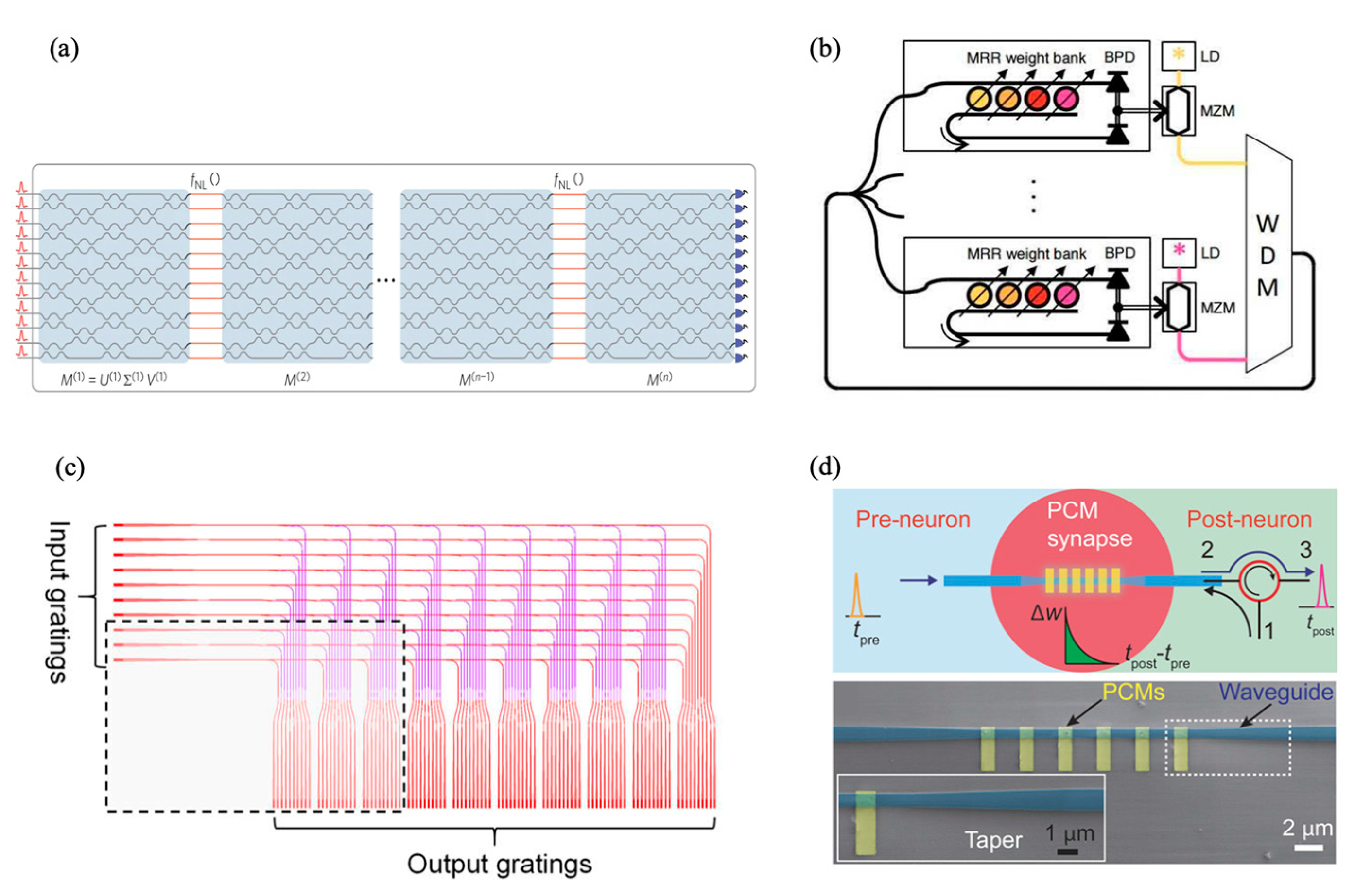
3.1. Silicon-Based Optical Neural Networks

More recently, the rapid development of silicon optical integration technology has provided technical support for research into photonic integrated neural network chips. Photonic integrated neural networks are used to perform matrix multiplication and addition calculations (MACs) in neural networks, using photon integration technology to run deep learning algorithms and implement machine learning-related applications. Conceptual exploratory research work has already been conducted on the use of photonic integrated neural network chips to implement neural network operations, and there is the hope of using photonic integrated neural network chips to accomplish tasks such as image classification and object detection for applications in servers, autonomous driving, and other scenarios. Representative research schemes include the Mach–Zehnder modulator scheme [33,34,35,36,37,38], micro-loop modulator scheme [39,40], and the three-dimensional integration scheme [41]. Such research has focused on simulation modeling and experimental applications of photonic neural network chips. In 2019, Lightelligence released the world’s first prototype board for photonic integrated neural network chips, which were then used to implement the MNIST handwritten digital dataset recognition application with a recognition accuracy of over 90% and a speed approximately two orders of magnitude faster than that of traditional electric chips, encouraging photonic integrated neural network chip applications and development. The number of Mach–Zehnder interferometers (MZIs) is proportional to the square number of elements N in a vector and is a necessary side effect of solving arbitrary matrices [33,36]. Loss, noise, and defects are serious problems that affect a system as the size of a photonic circuit increases [42].
Contemporary deep neural network architectures consist of linear cascades of layers followed by multiple iterations of nonlinear activation functions. Nonetheless, meshes based on devices such as MZIs, while capable of arbitrary matrix multiplication, cannot perform important nonlinear operations. As an alternative to MZI-based MACs, SiN-conjugated waveguides can be used to construct a fully optical neurosynaptic network that is based on phase change materials (PCMs) [43,44,45,46,47]. By varying the number of optical pulses to set the weights randomly, the time delay can modulate the weights to achieve a nonlinear activation function similar to a rectified linear unit with a synaptic plasticity consistent with the well-known Hebbian learning or spike-dependent plasticity rule [48]. Optical neural networks are based on silicon integration as shown in Figure 1.
Photonic neural networks offer a promising alternative to microelectronic and hybrid optoelectronic implementations, where classical neural networks rely heavily on fixed matrix multiplication. However, the need for phase stabilization and many neurons with large optical components, such as fibers and lenses, has been a major obstacle to achieving this conversion. Integrated photonics solves this problem by providing a scalable solution. Photon particles are too large to be integrated at the same high level as electrons [49]. In addition, present optical neural network solutions inevitably rely on electronics. Submicron-scale etching techniques are still not available, and height differences and spacing between optics and electronics and process incompatibilities make optoelectronic integration challenging. Furthermore, nonlinear limitations and photonics integration constraints make it impossible to scale chips such as electronic neuromorphic computing chips, which are mere arrays. In addition, nonvolatile photonic storage and weighting, as well as low power consumption, are necessary to ensure neurosynaptic functions [50,51]. Even though photonic nonlinear neural operations have been demonstrated in materials such as PCMs, there is still a large gap to electronic nonlinear neuromorphic operations, and there is still room for development in the energy efficiency and fast switching of new cumulable materials. As of yet, the goal of a large-scale, rapidly reprogrammable photonic neural network chip remains unrealized.

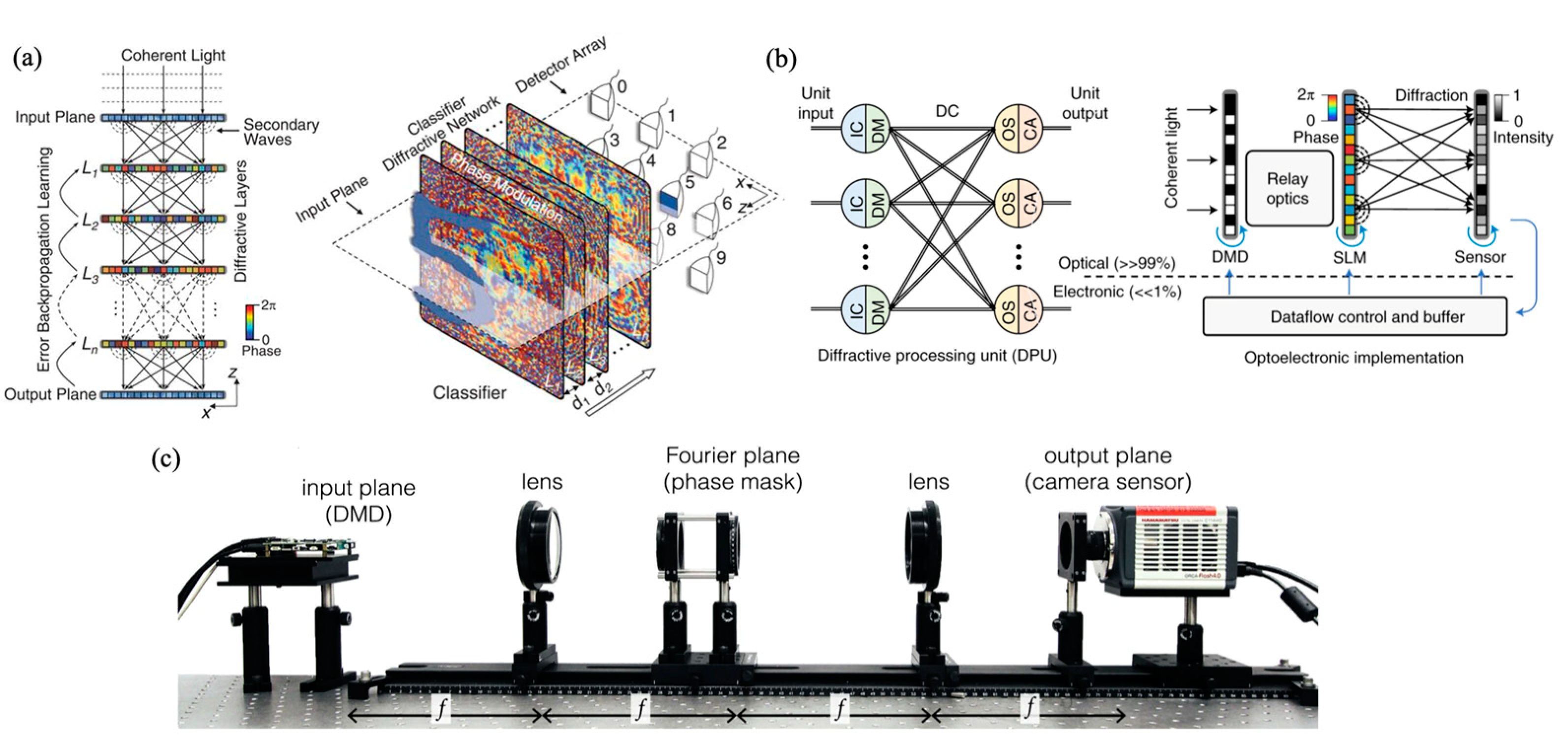
3.2. Deep Diffraction Neural Networks

Optical neural networks have been studied in Fourier optics for decades, and the forward physical structure of multilayer coherent neural networks is thought to be promising [18,52,53]. Deep diffraction neural networks (D2NNs) have been proposed for various classification tasks and can approach high-dimensional information capacity via optical processing, with millions of neurons and hundreds of billions of connections [54,55,56,57,58,59,60,61]. D2NNs also enable image saliency detection in Fourier space [53,62,63,64,65]. Diffraction is a prevalent physical phenomenon of incoherent light propagation, as seen in Figure 2. Any point in the plane perpendicular to the direction of propagation can be interpreted as a coherent superposition of complex amplitudes of integral points in the reference plane with a certain diffraction distance [66]. The superposition of diffraction meets the basic requirements of deep complex neural networks. Therefore, as an optical mechanism, coherent diffraction can provide an alternative method to fully connect multi-valued neurons. The training input of the underlying D2NN model is operated via spatial features. The input domain is filtered in the object or Fourier space by introducing a series of ordered passive filters prior to the diffraction network. This allows for the parallel processing of optical information.
D2NNs do not have nonlinear capabilities. In a D2NN made of linear materials, nonlinear optical processes, including surface nonlinearity, are negligible. The only form of nonlinearity in the forward optical model occurs in the photoelectron detector plane [53,67]. Deep neural networks using this scheme are capable of inference only for fixed tasks. Nonlinear operations are an indispensable and vital part of neuromorphic computing. Training, one of the key steps in the vast majority of neural network algorithms, has still not been implemented for such networks [68]. Optical neural networks are a promising energy-efficient method for implementing matrix multiplication. However, in practice, the neural network needs to be trained to be applied and cannot be implemented on hardware in which information can only flow in the forward direction.

3.3. Fiber-Based Optical Neural Networks
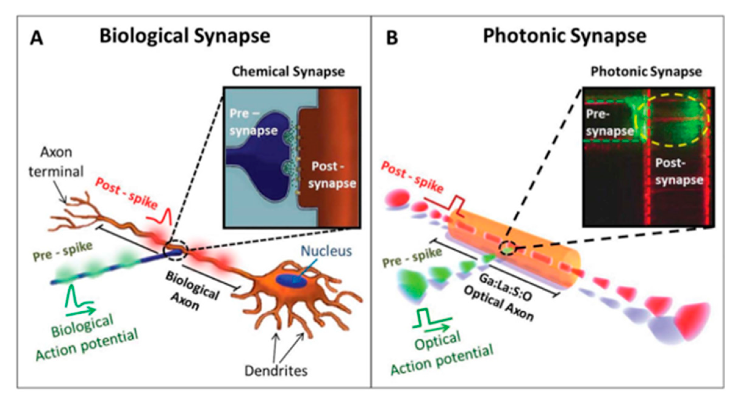
The human brain is complex, with 1011 neurons and 1015 synapses occupying a minimal space and consuming very little power. The average power consumption of a human brain is only 15 W [69]. In addition, the human brain is thought to be the fastest and most intelligent processing system in existence. The human brain relies on an interconnected network of organic biological microfibers, also known as neurons, to propagate information through the body. Using electrical action potentials, these signals are processed via different spatiotemporal principles [70].
Optical fibers have been widely used in communication, sensors, and illumination since the 1970s. Optical fibers are used as a transmission medium to transmit information via light. Optical fibers work similarly to biological neurons, where the neurons are activated by the input information and recognize it. The following section focuses on applying and developing optical fibers in neural networks.

3.3.1. Microfibers

Throughout the years, the field of neuromorphic engineering has been dedicated to the development of practical artificial neurocomputing devices that mimic the functions of the biological brain. To date, neuromorphic systems have been demonstrated with software running on conventional computers or complex electronic circuit configurations [43,71,72]. However, the efficiency of such systems is low compared with that of human neuromorphic systems. Accordingly, the search for alternative materials and structures to achieve efficient neuromorphic components is an area of intense research.
Optical fibers have been implemented in functional materials such as semiconductor compounds [73,74,75]. The physical properties of sulfur-based alloys are of interest because they are altered by light and exhibit brain-like functions in terms of plasticity and their form of transmission [76,77,78]. The signals of this type of microfiber display characteristics of biological signals transmitted in the brain via light transmission as seen in Figure 3 [79,80,81]. In addition, microfibers can monitor neural activity on the cortical surface and in deep brain regions [82,83]. Accordingly, microfibers appear to be a competitive category of artificial neuromorphic components and will likely be widely used in neuroscience research and medical applications in the future.

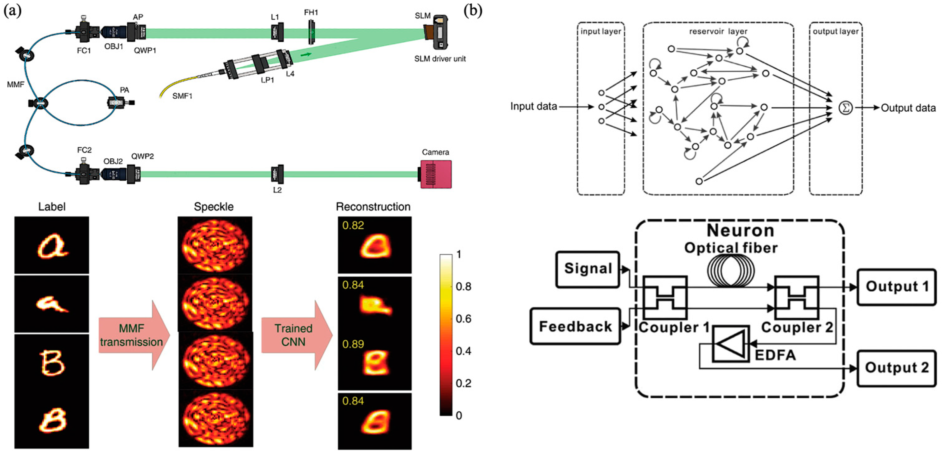
3.3.2. Multimode Fibers
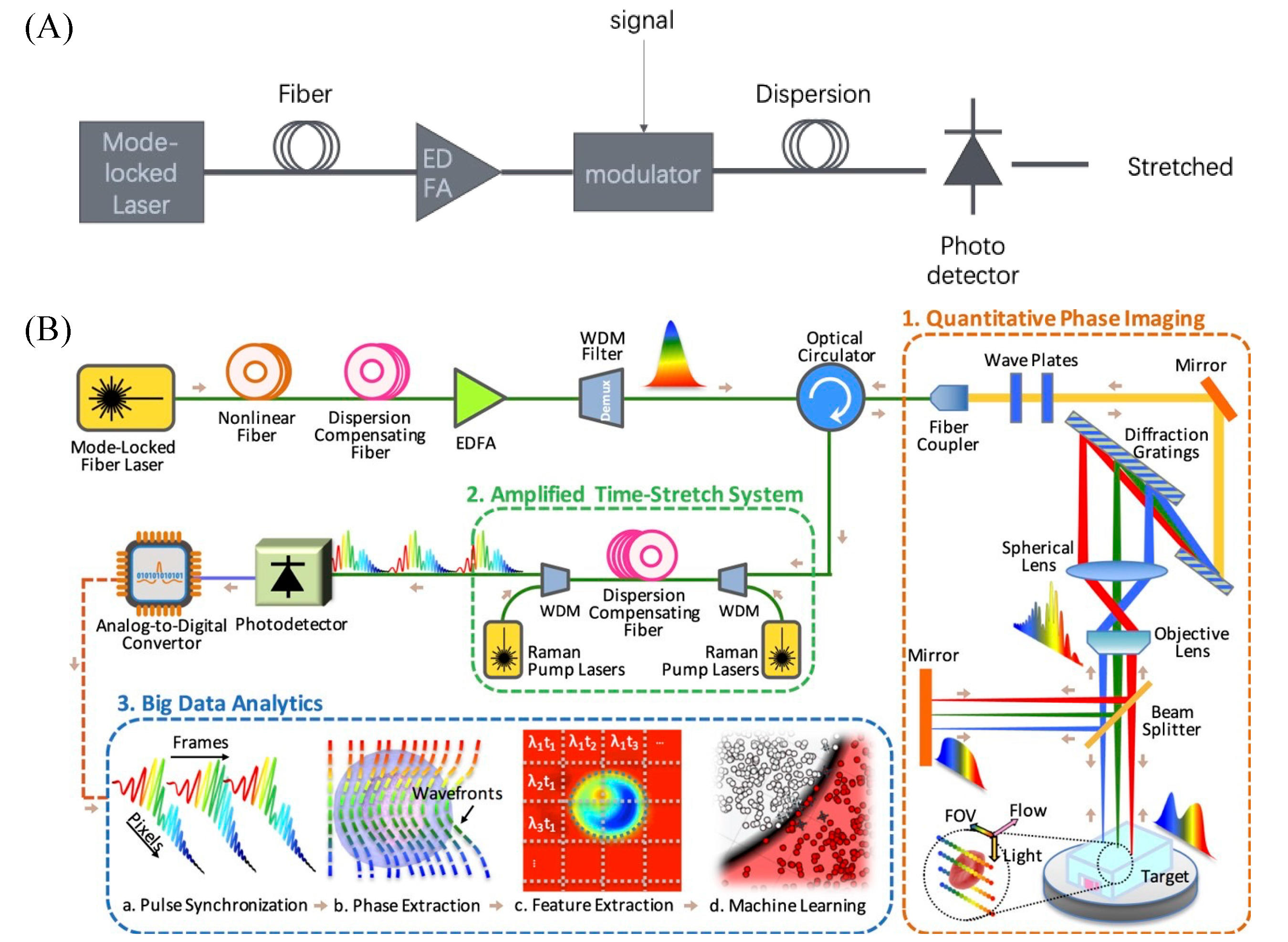
Since the 1980s, researchers have been studying the effect of scattering media on imaging systems and have found it possible to conduct imaging using the scattering media itself. The results indicate that imaging via scattering media not only improves the resolution of the imaging system but also eliminates image noise. Single-fiber imaging can be achieved if an optical fiber is treated as a scattering medium [84]. A multimode fiber (MMF) is a highly scattering medium that disrupts the light propagating through it and outputs speckle patterns that the human eye cannot decode. These patterns are called scattered spots. The behavior of a system consisting of input patterns has deterministic propagation through an MMF and a detector [85]. Multiple studies have shown that image sending or imaging through an MMF can be performed by simulating phase conjugation. With the development of digital holography and the increasing maturity of spatial light modulation devices and digital micromirror devices, beam wavefront and phase adjustments are becoming increasingly flexible and precise [86]. The proposed systems suffer from overly complex optical components and image distortion, resulting from variations in the path length experienced by the various modes of light propagation in optical fibers. Such problems can be effectively solved using neural networks. The idea of combining MMF imaging with neural networks for image classification has been around for more than three decades [87,88].
Currently, deep learning applications can solve more complex problems, and MMFs are becoming one of the choices available for optically implemented neural networks, as seen in Figure 4. The concept of combining a complex fix mapping with a simple programmable processor to achieve a powerful overall system has been applied to a variety of deep learning algorithms. Optical neural networks based on MMFs learn the nonlinear relationship between the amplitude of the scatter pattern obtained at the fiber output and the phase or amplitude at the fiber input [89,90,91]. In addition, optical reservoir computing (RC) systems have been shown to significantly improve the computational performance [92]. The reservoir layer of an all-optical reservoir computing system consists of an optical fiber and other optical process devices, and nonlinearity is reflected in the system. No electro-optical conversions are required in the reservoir layer, which dramatically reduces the problem of time consumption [93,94,95,96,97,98,99]. What is more, a picosecond-pulsed fiber laser is used to illuminate the subject, and the spatial information of the detected image is expanded in the time domain by using the inter-mode dispersion property of the multimode fiber. Time domain information is accordingly detected using a single-pixel detector, and the resulting two-dimensional image information can then ultimately be recovered from the one-dimensional time domain information with a neural network training method [100].
The key challenge when designing a viable optical neuromorphic computer is to combine the linear part of the optical system with the nonlinear elements and input–output interfaces while maintaining the speed and power efficiency of the optical interconnect. It is possible to combine the linear and nonlinear portions of an optical system in the shared body of an MMF. At the same time, a large number of spatial modes are densely supported in the MMF, maintaining the traditional high parallelism of optics while retaining the compact form factor. Therefore, it appears that MMF-based analog optical computers can be highly energy-efficient and versatile while having performance comparable to digital computers.

3.3.3. Time Stretch

Photonic time stretch (PTS) has been developing for more than two decades since its introduction in the 1990s [101]. It has become a mature optical technology that can slow down, amplify, and capture ultrafast events by slowing down the optical signal in real-time to bridge the bandwidth gap between electronics and photonics. PTS consists of a dispersive optical link that uses group velocity dispersion to convert the spectrum of a broadband optical pulse into a time-stretched temporal waveform. This method is used to perform Fourier transforms of the optical signal at a high frame rate on a single transmission basis for real-time analyses of fast dynamic processes. Via dispersion, the information residing in the spectrum is stretched over time. Group delay dispersion for time stretching can be experimentally implemented using various different device designs. The main designs of the proposed devices are internal Raman amplified fibers, chirped fiber Bragg gratings, array optical waveguide gratings, multimode waveguides (fiber or a pair of planar reflectors), and curved spatially mapped chromatic dispersion devices [102,103].
Deep learning extracts patterns and information from rich multidimensional datasets and is widely used for image recognition. Its earliest combination with PTS was for recognizing and classifying large numbers of cells. The Optical Fluid Time-Stretch Quantitative Phase Imaging (OTS-QPI) system reconstructs bright-field and quantitative phase images of flowing cells based on spectral interferograms of time-stretch light pulses, captures images of flowing cells with minimal motion distortion at rates greater than 10,000 cells/s, and extracts multiple biophysical features of individual cells, making it a powerful instrument for biomedical applications [104,105,106,107,108]. OTS-QPI was first implemented in combination with fully connected neural networks for image classification as seen in Figure 5A [104]. In addition, with the rapid development of deep learning and convolutional neural networks, combinations with generative adversarial networks and other image enhancement algorithms have been proposed to solve additional deep learning problems, combined with PTS [109,110].
Deep learning has evolved to the point where there is an urgent need for computationally small, low-latency datasets to reduce the computational effort associated with computational power limits and large datasets. When inputting data, nonlinear optical dynamics enables linear learning algorithms to learn nonlinear functions or determine boundaries to classify the data into correct classes. The nonlinear Schrödinger kernel, also called the Lambda kernel, is the core of this system [111,112]. The Lambda kernel, as seen in Figure 5B, is capable of nonlinearly casting data that have been modulated onto the spectrum of femtosecond pulses into a space where data that are non-dividable in linear terms are converted to be linearly divisible in the new space. In terms of functionality, there are similarities between the Lambda kernel and the concept of “kernel projection” in the machine learning literature. Using this approach, the spectrum of the data is mapped onto femtosecond light pulses and projected into an implicit high-dimensional space using nonlinear optical dynamics, thereby improving the accuracy and reducing the latency in the data classification by several orders of magnitude. The nonlinear dynamics are introduced into the data before processing the output data with an optical classifier.
Fiber optic imaging and nonlinear phenomena have been popular research topics in the field of optics. Control of the nonlinear propagation under spatiotemporal conditions can be achieved via mechanical perturbation of the fiber or by shaping the pumped light. Such an approach enables optically controllable computation within nonlinear optical fibers. Meanwhile, optical neural networks of optical fibers have good energy efficiency and scalability, providing a favorable approach for photonic neuromorphic computations.
Photonic integration renders ultrafast artificial neural networks possible, and photonic neuromorphic computing results in challenges different from those of electronic computing. Algorithms running on such hardware can meet the growing demand for deep learning and artificial intelligence in areas such as medical diagnostics, telecommunications, and high-performance and scientific computing. All calculations will be performed at the speed of light, which is much faster than the analog speed of digital computers, therefore processing exponentially more data. For real-time observations, time-stretch processors are ideal output devices. Even though photonic neuromorphic computing is still in its infancy, this research area has great potential to expand the frontiers of deep learning and information processing.
In this article, we highlight the diversity of optical neural networks. Optical neural networks are a rapidly growing field, with many schemes currently under investigation, all of which have their own advantages and disadvantages, as shown in Table 1.
Photonic neuromorphic computing is a system comprising active and passive devices, light sources, and transistors. However, no fabrication platform is yet capable of implementing all of these functions upon a single mold based on current fabrication levels. Present optical neural network solutions still exclusively rely on electronics. Optoelectronic integration processes remain challenging because submicron-scale etching techniques are still unavailable, and issues such as height disparities, spacing restrictions, and process incompatibilities are still prevalent. Currently, on-chip light sources use a concatenation of III–V families of materials or a direct epitaxy of quantum dot lasers on silicon. However, the complexity of the preparation process and associated reliability cannot meet the commercial mass production standards. Several approaches for integrating photonic systems and CMOS sensors for ultimately achieving a successful on-chip photonic neural network design are presently being explored.
Difficulties associated with on-chip optical delays are also a challenge being evaluated currently. Nonlinear operations are an indispensable and important part of neuromorphic computing. Moreover, nonvolatile photonic storage and weighting as well as low power consumption are necessary to ensure neurosynaptic function. Although photonic nonlinear neural operations have been demonstrated in materials such as PCM, a large gap still remains regarding electronic nonlinear neuromorphic operations. Accordingly, there is still room for development in energy efficiency and fast switching of new accumulable materials. In addition, training is one of the key steps for the vast majority of neural network algorithms, which to date still requires implementation.
Optical neural networks have been shown to be a promising energy-efficient method for implementing matrix multiplication [33,34]. However, these neural networks must be trained to be applied in practice, and they cannot be applied in hardware where information can flow in only the forward direction. Finally, current photonic platforms lack the common and important storage in electronic computers. In adaptive learning and training, weights need to be updated frequently, a situation that requires fast memories such as Dynamic Random Access Memory (DRAM), Resistive Random Access Memory (RRAM), and Ferroelectric Random Access Memory (FRAM). In summary, neuromorphic photonic systems can follow the same architecture, and the fabrication of stand-alone all-optical computers is therefore unlikely, owing to the lack of photonic memory devices.
In addition to being popular candidates for neuromorphic systems, optical neural networks exhibit several advantages. Neuromorphic processors are massively distributed hardware. Therefore, they heavily rely on parallel interconnections such as those which exist between components. Optical computing for neural network computation has the advantages of low latency, low power consumption, and high bandwidth, while the use of optical interconnections can offset the disadvantages of requiring broadband in electronic devices in exchange for interconnectivity. In addition, photonic synaptic devices modulated via photonic signals can simulate retinal neurons in the real eye, and physical device computing is conceptually close to the visual system and brain computing to simulate complex neural functions through optical modulation. Furthermore, the use of optical fiber can solve the problem of on-chip optical delays. In the future, co-packaging with electronic memory can be used to solve the existing challenges.

4. Discussion

The demand for increased data processing volumes and operation speeds is constantly growing, and it is urgent to circumvent the structural von Neumann bottleneck and design new structures to accommodate efficient neural network training and testing. Optical processors, with their advantages of high speeds and low power consumption, have been gaining attention as a result of the rapid development of hardware dedicated to the inference and training of optical neural networks. Optical neural networks have shown great promise in terms of low-energy consumption and high-speed parallel computing, and the development trend of optical neuromorphic computing appears to be unstoppable. According to research findings, photonic neuromorphic computing is currently in its preliminary developmental stage, and various optimization solutions have emerged, even though photonic neural networks still have many challenges to overcome.
In this paper, we reviewed the development of optical neural networks, emphasized optical neural networks with fiber dispersion, and provided some perspectives for the future development of optical neuromorphic computing (Table 1). Compared with other optical neural networks, optical neural networks with fiber dispersion have better nonlinear performance and neuron-like properties, thus exhibiting greater potential value. As optical technology matures, deep learning will further evolve with enhanced neuromorphic computing and optical neural networks as well as the application of increasingly high-performance integrated optics. In the future, hyper-scale and programmable optical neural networks will likely be implemented and applied to speech processing, image recognition, and target tracking, which will provide a bright future for neuromorphic photonics.

Author Contributions

Resources, D.Z.; data curation, D.Z.; writing—original draft preparation, D.Z.; writing—review and editing, D.Z. and Z.T.; supervision, Z.T.; project administration, Z.T.; funding acquisition, Z.T. All authors have read and agreed to the published version of the manuscript.

Funding

This research was funded by the National Natural Science Foundation of China (61875008).

Conflicts of Interest

The authors declare no conflict of interest.

References

  1. Hemanth, D.J.; Estrela, V.V. Deep Learning for Image Processing Applications; IOS Press: Amsterdam, The Netherlands, 2017; Volume 31. [Google Scholar]
  2. Huggins, W.J.; McClean, J.R.; Rubin, N.C.; Jiang, Z.; Wiebe, N.; Whaley, K.B.; Babbush, R. Efficient and noise resilient measurements for quantum chemistry on near-term quantum computers. NPJ. Quantum Inf. 2021, 7, 23. [Google Scholar] [CrossRef]
  3. Young, T.; Hazarika, D.; Poria, S.; Cambria, E. Recent trends in deep learning based natural language processing. IEEE Comput. Intell. Mag. 2018, 13, 55–75. [Google Scholar] [CrossRef]
  4. LeCun, Y.; Bengio, Y.; Hinton, G. Deep learning. Nature 2015, 521, 436–444. [Google Scholar] [CrossRef] [PubMed]
  5. Goodfellow, I.; Bengio, Y.; Courville, A. Deep Learning; MIT Press: Cambridge, MA, USA, 2016. [Google Scholar]
  6. Simonyan, K.; Zisserman, A. Very deep convolutional networks for large-scale image recognition. arXiv 2014, arXiv:1409.1556. [Google Scholar]
  7. Jouppi, N.P.; Young, C.; Patil, N.; Patterson, D.; Agrawal, G.; Bajwa, R.; Bates, S.; Bhatia, S.; Boden, N.; Borchers, A.; et al. In-datacenter performance analysis of a tensor processing unit. In Proceedings of the 44th Annual International Symposium on Computer Architecture, Toronto, ON, Canada, 24–28 June 2017; pp. 1–12. [Google Scholar]
  8. Basu, J.K.; Bhattacharyya, D.; Kim, T.H. Use of artificial neural network in pattern recognition. Int. J. Softw. Eng. Appl. 2010, 4. [Google Scholar]
  9. De Vries, A. Bitcoin’s growing energy problem. Joule 2018, 2, 801–805. [Google Scholar] [CrossRef] [Green Version]
  10. Prucnal, P.R.; Shastri, B.J.; Teich, M.C. Neuromorphic Photonics; CRC Press: Boca Raton, FL, USA, 2017. [Google Scholar]
  11. Padovani, A.; Woo, J.; Hwang, H.; Larcher, L. Understanding and optimization of pulsed SET operation in HfO x-based RRAM devices for neuromorphic computing applications. IEEE Electron Device Lett. 2018, 39, 672–675. [Google Scholar] [CrossRef]
  12. Eltes, F.; Villarreal-Garcia, G.E.; Caimi, D.; Siegwart, H.; Gentile, A.A.; Hart, A.; Stark, P.; Marshall, G.D.; Thompson, M.G.; Barreto, J.; et al. An integrated optical modulator operating at cryogenic temperatures. Nat. Mater. 2020, 19, 1164–1168. [Google Scholar] [CrossRef]
  13. Ying, Z.; Wang, Z.; Zhao, Z.; Dhar, S.; Pan, D.Z.; Soref, R.; Chen, R.T. Silicon microdisk-based full adders for optical computing. Opt. Lett. 2018, 43, 983–986. [Google Scholar] [CrossRef]
  14. Solli, D.R.; Jalali, B. Analog optical computing. Nat. Photonics 2015, 9, 704–706. [Google Scholar] [CrossRef]
  15. Sawchuk, A.A.; Strand, T.C. Digital optical computing. Proc. IEEE 1984, 72, 758–779. [Google Scholar] [CrossRef]
  16. Mennel, L.; Symonowicz, J.; Wachter, S.; Polyushkin, D.K.; Molina-Mendoza, A.J.; Mueller, T. Ultrafast machine vision with 2D material neural network image sensors. Nature 2020, 579, 62–66. [Google Scholar] [CrossRef] [PubMed]
  17. Psaltis, D.; Farhat, N. Optical information processing based on an associative-memory model of neural nets with thresholding and feedback. Opt. Lett. 1985, 10, 98–100. [Google Scholar] [CrossRef] [PubMed] [Green Version]
  18. Caulfield, H.J.; Kinser, J.; Rogers, S.K. Optical neural networks. Proc. IEEE 1989, 77, 1573–1583. [Google Scholar] [CrossRef]
  19. Denz, C. Optical Neural Networks; Springer Science & Business Media: Berlin/Heidelberg, Germany, 2013. [Google Scholar]
  20. Lee, L.S.; Stoll, H.; Tackitt, M. Continuous-time optical neural network associative memory. Opt. Lett. 1989, 14, 162–164. [Google Scholar] [CrossRef] [PubMed]
  21. Farhat, N.H.; Psaltis, D.; Prata, A.; Paek, E. Optical implementation of the Hopfield model. Appl. Opt. 1985, 24, 1469–1475. [Google Scholar] [CrossRef] [PubMed]
  22. Lu, T.T.; Francis, T.; Gregory, D.A. Self-organizing optical neural network for unsupervised learning. Opt. Eng. 1990, 29, 1107–1113. [Google Scholar] [CrossRef]
  23. Hinton, G.E. Deep belief networks. Scholarpedia 2009, 4, 5947. [Google Scholar] [CrossRef]
  24. LeCun, Y.; Bottou, L.; Bengio, Y.; Haffner, P. Gradient-based learning applied to document recognition. Proc. IEEE 1998, 86, 2278–2324. [Google Scholar] [CrossRef] [Green Version]
  25. Krizhevsky, A.; Sutskever, I.; Hinton, G.E. Imagenet classification with deep convolutional neural networks. Adv. Neural Inf. Process. Syst. 2012, 60, 84–90. [Google Scholar] [CrossRef]
  26. Szegedy, C.; Liu, W.; Jia, Y.; Sermanet, P.; Reed, S.; Anguelov, D.; Erhan, D.; Vanhoucke, V.; Rabinovich, A. Going deeper with convolutions. In Proceedings of the IEEE Conference on Computer Vision and Pattern Recognition, Boston, MA, USA, 7–12 June 2015; pp. 1–9. [Google Scholar]
  27. Szegedy, C.; Ioffe, S.; Vanhoucke, V.; Alemi, A.A. Inception-v4, inception-resnet and the impact of residual connections on learning. In Proceedings of the Thirty-First AAAI Conference on Artificial Intelligence, San Francisco, CA, USA, 4–9 February 2017. [Google Scholar]
  28. Mateen, M.; Wen, J.; Song, S.; Huang, Z. Fundus image classification using VGG-19 architecture with PCA and SVD. Symmetry 2018, 11, 1. [Google Scholar] [CrossRef] [Green Version]
  29. Anand, R.; Shanthi, T.; Nithish, M.; Lakshman, S. Face recognition and classification using GoogleNET architecture. In Soft Computing for Problem Solving; Springer: Berlin/Heidelberg, Germany, 2020; pp. 261–269. [Google Scholar]
  30. Thomson, D.; Zilkie, A.; Bowers, J.E.; Komljenovic, T.; Reed, G.T.; Vivien, L.; Marris-Morini, D.; Cassan, E.; Virot, L.; Fédéli, J.M.; et al. Roadmap on silicon photonics. J. Opt. 2016, 18, 073003. [Google Scholar] [CrossRef]
  31. Majumder, A.; Shen, B.; Polson, R.; Menon, R. Ultra-compact polarization rotation in integrated silicon photonics using digital metamaterials. Opt. Express 2017, 25, 19721–19731. [Google Scholar] [CrossRef]
  32. Li, J.; Huang, X.; Gong, J. Deep neural network for remote-sensing image interpretation: Status and perspectives. Natl. Sci. Rev. 2019, 6, 1082–1086. [Google Scholar] [CrossRef]
  33. Shen, Y.; Harris, N.C.; Skirlo, S.; Prabhu, M.; Baehr-Jones, T.; Hochberg, M.; Sun, X.; Zhao, S.; Larochelle, H.; Englund, D.; et al. Deep learning with coherent nanophotonic circuits. Nat. Photonics 2017, 11, 441–446. [Google Scholar] [CrossRef]
  34. Hamerly, R.; Bernstein, L.; Sludds, A.; Soljačić, M.; Englund, D. Large-scale optical neural networks based on photoelectric 3multiplication. Phys. Rev. X 2019, 9, 021032. [Google Scholar]
  35. Fang, M.Y.S.; Manipatruni, S.; Wierzynski, C.; Khosrowshahi, A.; DeWeese, M.R. Design of optical neural networks with component imprecisions. Opt. Express 2019, 27, 14009–14029. [Google Scholar] [CrossRef] [Green Version]
  36. Pai, S.; Bartlett, B.; Solgaard, O.; Miller, D.A. Matrix optimization on universal unitary photonic devices. Phys. Rev. Appl. 2019, 11, 064044. [Google Scholar] [CrossRef] [Green Version]
  37. Bangari, V.; Marquez, B.A.; Miller, H.; Tait, A.N.; Nahmias, M.A.; De Lima, T.F.; Peng, H.T.; Prucnal, P.R.; Shastri, B.J. Digital electronics and analog photonics for convolutional neural networks (DEAP-CNNs). IEEE J. Sel. Top. Quantum Electron. 2019, 26, 1–13. [Google Scholar] [CrossRef] [Green Version]
  38. Tait, A.N.; De Lima, T.F.; Nahmias, M.A.; Miller, H.B.; Peng, H.T.; Shastri, B.J.; Prucnal, P.R. Silicon photonic modulator neuron. Phys. Rev. Appl. 2019, 11, 064043. [Google Scholar] [CrossRef] [Green Version]
  39. Huang, C.; Bilodeau, S.; Ferreira de Lima, T.; Tait, A.N.; Ma, P.Y.; Blow, E.C.; Jha, A.; Peng, H.T.; Shastri, B.J.; Prucnal, P.R. Demonstration of scalable microring weight bank control for large-scale photonic integrated circuits. APL Photonics 2020, 5, 040803. [Google Scholar] [CrossRef]
  40. Tait, A.N.; De Lima, T.F.; Zhou, E.; Wu, A.X.; Nahmias, M.A.; Shastri, B.J.; Prucnal, P.R. Neuromorphic photonic networks using silicon photonic weight banks. Sci. Rep. 2017, 7, 7430. [Google Scholar] [CrossRef] [PubMed]
  41. Chiles, J.; Buckley, S.M.; Nam, S.W.; Mirin, R.P.; Shainline, J.M. Design, fabrication, and metrology of 10 × 100 multi-planar integrated photonic routing manifolds for neural networks. APL Photonics 2018, 3, 106101. [Google Scholar] [CrossRef]
  42. Martens, D.; Bienstman, P. Study on the limit of detection in MZI-based biosensor systems. Sci. Rep. 2019, 9, 5767. [Google Scholar] [CrossRef] [Green Version]
  43. Cheng, Z.; Ríos, C.; Pernice, W.H.; Wright, C.D.; Bhaskaran, H. On-chip photonic synapse. Sci. Adv. 2017, 3, e1700160. [Google Scholar] [CrossRef] [Green Version]
  44. Feldmann, J.; Youngblood, N.; Wright, C.D.; Bhaskaran, H.; Pernice, W.H. All-optical spiking neurosynaptic networks with self-learning capabilities. Nature 2019, 569, 208–214. [Google Scholar] [CrossRef] [Green Version]
  45. Joshi, V.; Le Gallo, M.; Haefeli, S.; Boybat, I.; Nandakumar, S.R.; Piveteau, C.; Dazzi, M.; Rajendran, B.; Sebastian, A.; Eleftheriou, E. Accurate deep neural network inference using computational phase-change memory. Nat. Commun. 2020, 11, 2473. [Google Scholar] [CrossRef]
  46. Miscuglio, M.; Sorger, V.J. Photonic tensor cores for machine learning. Appl. Phys. Rev. 2020, 7, 031404. [Google Scholar] [CrossRef]
  47. Wu, C.; Yu, H.; Lee, S.; Peng, R.; Takeuchi, I.; Li, M. Programmable phase-change metasurfaces on waveguides for multimode photonic convolutional neural network. Nat. Commun. 2021, 12, 96. [Google Scholar] [CrossRef]
  48. Caporale, N.; Dan, Y. Spike timing–dependent plasticity: A Hebbian learning rule. Annu. Rev. Neurosci. 2008, 31, 25–46. [Google Scholar] [CrossRef] [Green Version]
  49. de Valicourt, G.; Chang, C.M.; Eggleston, M.S.; Melikyan, A.; Zhu, C.; Lee, J.; Simsarian, J.E.; Chandrasekhar, S.; Sinsky, J.H.; Kim, K.W.; et al. Photonic integrated circuit based on hybrid III–V/silicon integration. J. Lightwave Technol. 2017, 36, 265–273. [Google Scholar] [CrossRef]
  50. Guo, X.; He, A.; Su, Y. Recent advances of heterogeneously integrated III–V laser on Si. J. Semicond. 2019, 40, 101304. [Google Scholar] [CrossRef]
  51. Zhai, Y.; Yang, J.Q.; Zhou, Y.; Mao, J.Y.; Ren, Y.; Roy, V.A.; Han, S.T. Toward non-volatile photonic memory: Concept, material and design. Mater. Horiz. 2018, 5, 641–654. [Google Scholar] [CrossRef]
  52. Lin, X.; Rivenson, Y.; Yardimci, N.T.; Veli, M.; Luo, Y.; Jarrahi, M.; Ozcan, A. All-optical machine learning using diffractive deep neural networks. Science 2018, 361, 1004–1008. [Google Scholar] [CrossRef] [Green Version]
  53. Mengu, D.; Luo, Y.; Rivenson, Y.; Ozcan, A. Analysis of diffractive optical neural networks and their integration with electronic neural networks. IEEE J. Sel. Top. Quantum Electron. 2019, 26, 1–14. [Google Scholar] [CrossRef] [Green Version]
  54. Maktoobi, S.; Froehly, L.; Andreoli, L.; Porte, X.; Jacquot, M.; Larger, L.; Brunner, D. Diffractive coupling for photonic networks: How big can we go? IEEE J. Sel. Top. Quantum Electron. 2019, 26, 1–8. [Google Scholar] [CrossRef]
  55. Xiao, Y.L.; Li, S.; Situ, G.; You, Z. Unitary learning for diffractive deep neural network. Opt. Lasers Eng. 2021, 139, 106499. [Google Scholar] [CrossRef]
  56. Xiao, Y.L.; Liang, R.; Zhong, J.; Su, X.; You, Z. Compatible Learning for Deep Photonic Neural Network. arXiv 2020, arXiv:2003.08360. [Google Scholar]
  57. Zhao, Q.; Hao, S.; Wang, Y.; Wang, L.; Xu, C. Orbital angular momentum detection based on diffractive deep neural network. Opt. Commun. 2019, 443, 245–249. [Google Scholar] [CrossRef]
  58. Fu, T.; Zang, Y.; Huang, H.; Du, Z.; Hu, C.; Chen, M.; Yang, S.; Chen, H. On-chip photonic diffractive optical neural network based on a spatial domain electromagnetic propagation model. Opt. Express 2021, 29, 31924–31940. [Google Scholar] [CrossRef]
  59. Lu, L.; Zhu, L.; Zhang, Q.; Zhu, B.; Yao, Q.; Yu, M.; Niu, H.; Dong, M.; Zhong, G.; Zeng, Z. Miniaturized diffraction grating design and processing for deep neural network. IEEE Photonics Technol. Lett. 2019, 31, 1952–1955. [Google Scholar] [CrossRef]
  60. Bernstein, L.; Sludds, A.; Hamerly, R.; Sze, V.; Emer, J.; Englund, D. Freely scalable and reconfigurable optical hardware for deep learning. Sci. Rep. 2021, 11, 3144. [Google Scholar] [CrossRef] [PubMed]
  61. Zhou, T.; Lin, X.; Wu, J.; Chen, Y.; Xie, H.; Li, Y.; Fan, J.; Wu, H.; Fang, L.; Dai, Q. Large-scale neuromorphic optoelectronic computing with a reconfigurable diffractive processing unit. Nat. Photonics 2021, 15, 367–373. [Google Scholar] [CrossRef]
  62. Li, J.; Mengu, D.; Luo, Y.; Rivenson, Y.; Ozcan, A. Class-specific differential detection in diffractive optical neural networks improves inference accuracy. Adv. Photonics 2019, 1, 046001. [Google Scholar] [CrossRef] [Green Version]
  63. Yan, T.; Wu, J.; Zhou, T.; Xie, H.; Xu, F.; Fan, J.; Fang, L.; Lin, X.; Dai, Q. Fourier-space diffractive deep neural network. Phys. Rev. Lett. 2019, 123, 023901. [Google Scholar] [CrossRef]
  64. Rahman, M.S.S.; Li, J.; Mengu, D.; Rivenson, Y.; Ozcan, A. Ensemble learning of diffractive optical networks. Light Sci. Appl. 2021, 10, 14. [Google Scholar] [CrossRef]
  65. Chang, J.; Sitzmann, V.; Dun, X.; Heidrich, W.; Wetzstein, G. Hybrid optical-electronic convolutional neural networks with optimized diffractive optics for image classification. Sci. Rep. 2018, 8, 12324. [Google Scholar] [CrossRef] [Green Version]
  66. Matsushima, K.; Schimmel, H.; Wyrowski, F. Fast calculation method for optical diffraction on tilted planes by use of the angular spectrum of plane waves. J. Opt. Soc. Am. A 2003, 20, 1755–1762. [Google Scholar] [CrossRef]
  67. Xiao, Y.; Qian, H.; Liu, Z. Nonlinear metasurface based on giant optical kerr response of gold quantum wells. ACS Photonics 2018, 5, 1654–1659. [Google Scholar] [CrossRef]
  68. Silva, I.N.D.; Hernane Spatti, D.; Andrade Flauzino, R.; Liboni, L.H.B.; Reis Alves, S.F.D. Artificial neural network architectures and training processes. In Artificial Neural Networks; Springer: Berlin/Heidelberg, Germany, 2017; pp. 21–28. [Google Scholar]
  69. Marković, D.; Mizrahi, A.; Querlioz, D.; Grollier, J. Physics for neuromorphic computing. Nat. Rev. Phys. 2020, 2, 499–510. [Google Scholar] [CrossRef]
  70. Radivojevic, M.; Jäckel, D.; Altermatt, M.; Müller, J.; Viswam, V.; Hierlemann, A.; Bakkum, D.J. Electrical identification and selective microstimulation of neuronal compartments based on features of extracellular action potentials. Sci. Rep. 2016, 6, 31332. [Google Scholar] [CrossRef] [PubMed]
  71. Sokolov, A.S.; Abbas, H.; Abbas, Y.; Choi, C. Towards engineering in memristors for emerging memory and neuromorphic computing: A review. J. Semicond. 2021, 42, 013101. [Google Scholar] [CrossRef]
  72. Kim, S.G.; Han, J.S.; Kim, H.; Kim, S.Y.; Jang, H.W. Recent advances in memristive materials for artificial synapses. Adv. Mater. Technol. 2018, 3, 1800457. [Google Scholar] [CrossRef] [Green Version]
  73. Ballato, J.; Hawkins, T.; Foy, P.; Stolen, R.; Kokuoz, B.; Ellison, M.; McMillen, C.; Reppert, J.; Rao, A.; Daw, M.; et al. Silicon optical fiber. Opt. Express 2008, 16, 18675–18683. [Google Scholar] [CrossRef] [PubMed]
  74. Gambling, W.A. The rise and rise of optical fibers. IEEE J. Sel. Top. Quantum Electron. 2000, 6, 1084–1093. [Google Scholar] [CrossRef]
  75. Lu, P.; Lalam, N.; Badar, M.; Liu, B.; Chorpening, B.T.; Buric, M.P.; Ohodnicki, P.R. Distributed optical fiber sensing: Review and perspective. Appl. Phys. Rev. 2019, 6, 041302. [Google Scholar] [CrossRef]
  76. Pickett, M.D.; Medeiros-Ribeiro, G.; Williams, R.S. A scalable neuristor built with Mott memristors. Nat. Mater. 2013, 12, 114–117. [Google Scholar] [CrossRef]
  77. Shi, J.; Ha, S.D.; Zhou, Y.; Schoofs, F.; Ramanathan, S. A correlated nickelate synaptic transistor. Nat. Commun. 2013, 4, 2676. [Google Scholar] [CrossRef] [Green Version]
  78. Wright, C.D.; Au, Y.Y.; Aziz, M.M.; Bhaskaran, H.; Cobley, R.; Rodriguez-Hernandez, G.; Hosseini, P.; Pernice, W.H.; Wang, L. Novel Applications Possibilities for Phase-Change Materials and Devices. 2013. Available online: http://hdl.handle.net/10871/20347 (accessed on 5 April 2022).
  79. Gholipour, B.; Zhang, J.; MacDonald, K.F.; Hewak, D.W.; Zheludev, N.I. An all-optical, non-volatile, bidirectional, phase-change meta-switch. Adv. Mater. 2013, 25, 3050–3054. [Google Scholar] [CrossRef]
  80. Gholipour, B.; Bastock, P.; Craig, C.; Khan, K.; Hewak, D.; Soci, C. Amorphous metal-sulphide microfibers enable photonic synapses for brain-like computing. Adv. Opt. Mater. 2015, 3, 635–641. [Google Scholar] [CrossRef]
  81. Ramos, M.; Bharadwaj, V.; Sotillo, B.; Gholipour, B.; Giakoumaki, A.N.; Ramponi, R.; Eaton, S.M.; Soci, C. Photonic implementation of artificial synapses in ultrafast laser inscribed waveguides in chalcogenide glass. Appl. Phys. Lett. 2021, 119, 031104. [Google Scholar] [CrossRef]
  82. Miyamoto, D.; Murayama, M. The fiber-optic imaging and manipulation of neural activity during animal behavior. Neurosci. Res. 2016, 103, 1–9. [Google Scholar] [CrossRef] [PubMed] [Green Version]
  83. Schlegel, F.; Sych, Y.; Schroeter, A.; Stobart, J.; Weber, B.; Helmchen, F.; Rudin, M. Fiber-optic implant for simultaneous fluorescence-based calcium recordings and BOLD fMRI in mice. Nat. Protoc. 2018, 13, 840–855. [Google Scholar] [CrossRef]
  84. Fischer, B.; Sternklar, S. Image transmission and interferometry with multimode fibers using self-pumped phase conjugation. Appl. Phys. Lett. 1985, 46, 113–114. [Google Scholar] [CrossRef]
  85. Psaltis, D.; Moser, C. Imaging with multimode fibers. Opt. Photonics News 2016, 27, 24–31. [Google Scholar] [CrossRef]
  86. Vasquez-Lopez, S.A.; Turcotte, R.; Koren, V.; Plöschner, M.; Padamsey, Z.; Booth, M.J.; Cižmár, T.; Emptage, N.J. Subcellular spatial resolution achieved for deep-brain imaging in vivo using a minimally invasive multimode fiber. Light Sci. Appl. 2018, 7, 110. [Google Scholar] [CrossRef] [Green Version]
  87. Aisawa, S.; Noguchi, K.; Matsumoto, T. Remote image classification through multimode optical fiber using a neural network. Opt. Lett. 1991, 16, 645–647. [Google Scholar] [CrossRef]
  88. Marusarz, R.K.; Sayeh, M.R. Neural network-based multimode fiber-optic information transmission. Appl. Opt. 2001, 40, 219–227. [Google Scholar] [CrossRef]
  89. Rahmani, B.; Loterie, D.; Konstantinou, G.; Psaltis, D.; Moser, C. Multimode optical fiber transmission with a deep learning network. Light Sci. Appl. 2018, 7, 69. [Google Scholar]
  90. Caramazza, P.; Moran, O.; Murray-Smith, R.; Faccio, D. Transmission of natural scene images through a multimode fibre. Nat. Commun. 2019, 10, 2029. [Google Scholar] [CrossRef] [Green Version]
  91. Teğin, U.; Yıldırım, M.; Oğuz, İ.; Moser, C.; Psaltis, D. Scalable optical learning operator. Nat. Comput. Sci. 2021, 1, 542–549. [Google Scholar] [CrossRef]
  92. Tanaka, G.; Yamane, T.; Héroux, J.B.; Nakane, R.; Kanazawa, N.; Takeda, S.; Numata, H.; Nakano, D.; Hirose, A. Recent advances in physical reservoir computing: A review. Neural Netw. 2019, 115, 100–123. [Google Scholar] [CrossRef] [PubMed]
  93. Vandoorne, K.; Dierckx, W.; Schrauwen, B.; Verstraeten, D.; Baets, R.; Bienstman, P.; Van Campenhout, J. Toward optical signal processing using photonic reservoir computing. Opt. Express 2008, 16, 11182–11192. [Google Scholar] [CrossRef]
  94. Fiers, M.A.A.; Van Vaerenbergh, T.; Wyffels, F.; Verstraeten, D.; Schrauwen, B.; Dambre, J.; Bienstman, P. Nanophotonic reservoir computing with photonic crystal cavities to generate periodic patterns. IEEE Trans. Neural Netw. Learn. Syst. 2013, 25, 344–355. [Google Scholar] [CrossRef] [Green Version]
  95. Vinckier, Q.; Duport, F.; Smerieri, A.; Vandoorne, K.; Bienstman, P.; Haelterman, M.; Massar, S. High-performance photonic reservoir computer based on a coherently driven passive cavity. Optica 2015, 2, 438–446. [Google Scholar] [CrossRef]
  96. Mesaritakis, C.; Syvridis, D. Reservoir computing based on transverse modes in a single optical waveguide. Opt. Lett. 2019, 44, 1218–1221. [Google Scholar] [CrossRef]
  97. Scofield, A.C.; Sefler, G.A.; Shaw, T.J.; Valley, G.C. Recent results using laser speckle in multimode waveguides for random projections. Opt. Data Sci. 2019, 10937, 17–24. [Google Scholar]
  98. Cheng, T.Y.; Chou, D.Y.; Liu, C.C.; Chang, Y.J.; Chen, C.C. Optical neural networks based on optical fiber-communication system. Neurocomputing 2019, 364, 239–244. [Google Scholar] [CrossRef]
  99. Sunada, S.; Kanno, K.; Uchida, A. Using multidimensional speckle dynamics for high-speed, large-scale, parallel photonic computing. Opt. Express 2020, 28, 30349–30361. [Google Scholar] [CrossRef]
  100. Liu, Z.; Wang, L.; Meng, Y.; He, T.; He, S.; Yang, Y.; Wang, L.; Tian, J.; Li, D.; Yan, P.; et al. All-fiber high-speed image detection enabled by deep learning. Nat. Commun. 2022, 13, 1433. [Google Scholar] [CrossRef]
  101. Caputi, W.J. Stretch: A time-transformation technique. IEEE Trans. Aerosp. Electron. Syst. 1971, AES-7, 269–278. [Google Scholar] [CrossRef]
  102. Lei, C.; Guo, B.; Cheng, Z.; Goda, K. Optical time-stretch imaging: Principles and applications. Appl. Phys. Rev. 2016, 3, 011102. [Google Scholar] [CrossRef]
  103. Mahjoubfar, A.; Churkin, D.V.; Barland, S.; Broderick, N.; Turitsyn, S.K.; Jalali, B. Time stretch and its applications. Nat. Photonics 2017, 11, 341–351. [Google Scholar] [CrossRef]
  104. Chen, C.L.; Mahjoubfar, A.; Tai, L.C.; Blaby, I.K.; Huang, A.; Niazi, K.R.; Jalali, B. Deep learning in label-free cell classification. Sci. Rep. 2016, 6, 21471. [Google Scholar] [CrossRef] [Green Version]
  105. Wu, Y.; Zhou, Y.; Huang, C.J.; Kobayashi, H.; Yan, S.; Ozeki, Y.; Wu, Y.; Sun, C.W.; Yasumoto, A.; Yatomi, Y.; et al. Intelligent frequency-shifted optofluidic time-stretch quantitative phase imaging. Opt. Express 2020, 28, 519–532. [Google Scholar] [CrossRef]
  106. Mahjoubfar, A.; Chen, C.L.; Lin, J.; Jalali, B. AI-augmented time stretch microscopy. In Proceedings of the High-Speed Biomedical Imaging and Spectroscopy: Toward Big Data Instrumentation and Management II, San Francisco, CA, USA, 28 January–2 February 2017; Volume 10076, p. 10076J. [Google Scholar]
  107. Guo, B.; Lei, C.; Kobayashi, H.; Ito, T.; Yalikun, Y.; Jiang, Y.; Tanaka, Y.; Ozeki, Y.; Goda, K. High-throughput, label-free, single-cell, microalgal lipid screening by machine-learning-equipped optofluidic time-stretch quantitative phase microscopy. Cytom. Part A 2017, 91, 494–502. [Google Scholar] [CrossRef] [Green Version]
  108. Guo, B.; Lei, C.; Wu, Y.; Kobayashi, H.; Ito, T.; Yalikun, Y.; Lee, S.; Isozaki, A.; Li, M.; Jiang, Y.; et al. Optofluidic time-stretch23 quantitative phase microscopy. Methods 2018, 136, 116–125. [Google Scholar] [CrossRef]
  109. Lo, M.C.; Lee, K.C.; Siu, D.M.; Lam, E.Y.; Tsia, K.K. Augmented multiplexed asymmetric-detection time-stretch optical microscopy by generative deep learning. In Proceedings of the High-Speed Biomedical Imaging and Spectroscopy VI, Online, 6–12 March 2021; Volume 11654, p. 1165410. [Google Scholar]
  110. Suthar, M.; Jalali, B. Natural algorithms for image and video enhancement. In Proceedings of the AI and Optical Data Sciences II, Online, 6–12 March 2021; Volume 11703, p. 1170315. [Google Scholar]
  111. Zhou, T.; Scalzo, F.; Jalali, B. Nonlinear Schrodinger Kernel for hardware acceleration of machine learning. J. Lightwave Technol. 2022, 40, 1308–1319. [Google Scholar] [CrossRef]
  112. Jalali, B.; Zhou, T.; Scalzo, F. Time Stretch Computing for Ultrafast Single-shot Data Acquisition and Inference. In Proceedings of the 2021 Optical Fiber Communications Conference and Exhibition (OFC), Washington, DC, USA, 6–11 June 2021; pp. 1–3. [Google Scholar]
Figure 1. Implementing a neural network based on silicon integration. (a) A silicon photonic integrated circuit comprising programmable MZIs realizes the optical interference unit. This architecture enables the operation of the weight matrix using the MZIs through singular value decomposition [33]. (b) Using the micro-ring resonator as the neuron of the broadcast and weight network, the wavelength division multiplexed signals are weighted using reconfigurable continuous value filters and then summed for total power detection [40]. (c) A biplane signal distribution network is realized through the stacking of waveguides, which can complete the all-around connection of the feedforward neural network [41]. (d) Photonic synapses are fabricated using PCM in combination with an integrated silicon nitride waveguide, and the synaptic weights are set randomly by varying the number of optical pulses sent by the waveguide [43].
Applsci 12 05338 g001
Figure 2. Implementing D2NNs. (a) Several transmission or reflection layers are 3D printed, and each point on the layer is an artificial neuron with a given weight connected to other neurons in the next layer via optical diffraction [52]. (b) Diffractive process units (DPUs) are designed as a large-scale perceptron class optoelectronic computing building block that can be programmed to build different deep neural networks implemented with programmable optoelectronic devices, such as digital micromirror devices (DMDs), phased spatial light modulators (SLMs), and CMOS sensors [61]. (c) An optical convolutional layer with an optimizable phase mask is conceived to implement a convolutional neural network using the intrinsic convolution performed using a linear spatial non-turning image system [60].
Applsci 12 05338 g002
Figure 3. Comparison of photons with biological neurons and synapses [80]. (A,B) is biological synapse and photonic synapse, respectively.
Applsci 12 05338 g003
Figure 4. (a) CNNs project arbitrary patterns and perform transfer learning via MMF [89]. (b) MMF-based free-space all-optical RC system using spatial light modulators and diffractive optical elements [98].
Applsci 12 05338 g004
Figure 5. (A) PTS schematic diagram of principle. (B) OTS-QPI system operational process [104].
Applsci 12 05338 g005
Table 1. Comparison of the different approaches to optical neural networks.
TechnologyCategoriesAdvantagesDisadvantagesChip Capabilities
Silicon-based optical neural networksMach–Zehnder modulator schemeMatrix multiplication has high speed and low power consumptionO/E conversionInference
Micro-loop modulator scheme
3D integration scheme
D2NNOptical diffractionHandles large amounts of dataNot conducive to reuseInference
Fiber-based optical neural networksMicrofiberWavelength division multiplexing, biological-like neuronsLarge sizeNo chip
MMFIt has both linear and nonlinear functionsNot easy to control
PTSPhoton DACMassive system
Publisher’s Note: MDPI stays neutral with regard to jurisdictional claims in published maps and institutional affiliations.

