Article

Sliding-Mode Control of a Photovoltaic System Based on a Flyback Converter for Microinverter Applications

by
Carlos Andres Ramos-Paja
1,*,†,
Juan David Bastidas-Rodriguez
2,† and
Andres Julian Saavedra-Montes
1,†
1
Facultad de Minas, Universidad Nacional de Colombia, Medellin 050013, Colombia
2
Facultad de Ingeniería y Arquitectura, Universidad Nacional de Colombia, Manizales 170003, Colombia
*
Author to whom correspondence should be addressed.
These authors contributed equally to this work.
Appl. Sci. 2022, 12(3), 1399; https://doi.org/10.3390/app12031399
Submission received: 29 November 2021 / Revised: 15 January 2022 / Accepted: 20 January 2022 / Published: 28 January 2022

Abstract

:

Featured Application

Improve the dynamic response and perturbation rejection of two-stage flyback-based microinverters or flyback-based photovoltaic power optimizers.

Abstract

A method to design a sliding-mode control of a photovoltaic system based on a flyback converter is proposed. First, the photovoltaic system is modeled to design the sliding-mode controller and to select the parameters of a maximum power point tracking algorithm. Then, the detailed design of the sliding-mode controller is presented, which includes the establishment of the sliding surface. The transversality, reachability, and equivalent control tests are also developed. Because the power extraction of the PV system is carried out through a P&O MPPT algorithm, the selection of the perturbation magnitude, the perturbation period, and the maximum switching frequency is integrated into the control design. Additionally, since the derivative of the MPPT output could prevent the achievement of the reachability test, a filter to limit that derivative is also integrated into the design process. The whole method is illustrated in an application example where the data of a BP585 PV module and a real flyback converter are used. Once the parameters were obtained, circuital simulations performed in PSIM validated the intended operation of a PV system composed of a PV module and a flyback converter, which is connected to a source that produces the perturbations of an AC grid.

1. Introduction

Photovoltaic (PV) systems have been established as one of the most important renewable energy sources around the world in recent years, reaching a cumulative installed capacity of 760.4 G W , of which 139.4 G W were installed in 2020 [1]. Therefore, there is continuous research interest in improving power harvesting and mitigating the significant power reductions produced by non-homogeneous conditions over the PV arrays.
When a PV array is operating under homogeneous conditions, i.e., all the modules operate at the same irradiance and temperature, there is only one maximum power point (MPP) in its power vs. voltage (P–V) curve [2]. However, real PV arrays operate under non-homogeneous conditions due to partial shading, soiling, not uniform aging, differences in the characteristics of the modules, etc. These non-homogeneous conditions generate multiple MPPs in the array P–V curve, where the global MPP (GMPP) is considerably smaller than the sum of the maximum power that can be produced by each module [2].
There are two main architectures to mitigate the power losses produced by non-homogeneous conditions. The first one uses a string or array inverter with an MPP tracking (MPPT) algorithm that is able to track the GMPP even if the array is operating under time-varying non-homogeneous conditions. However, those systems cannot extract all the power available in the PV modules since non-homogeneous conditions activate one or more bypass diodes in the PV modules, which avoids the power harvesting from the bypassed sub-modules [3].
The second architecture to mitigate the power losses produced by non-homogeneous conditions uses one inverter, called a microinverter, for each module, which allows the direct connection of a PV module to the grid. These devices allow the extraction of the maximum power from each module and reduce the number of active bypass diodes; as a consequence, there is an increment in the power production from an array operating in non-homogeneous conditions [4]. Moreover, microinverters provide a flexible design, commissioning, and maintenance of the PV system since each set module-microinverter can be independently connected and disconnected from the grid without de-energizing the whole string or array. Additionally, microinverters improve the system reliability because the failure of one set module-microinverter does not affect the rest of the system. Additionally, microinverters also increase safety because they avoid the presence of high dc voltages [5].
A microinverter is typically formed by two power stages connected through a dc-link capacitor [4]. The first stage is formed by a dc/dc converter with high voltage gain to generate the dc bus voltage required by the inverter (e.g., 200 V [6], 240 V [7], 311 V [8], 380 V [9], and 400 V [10]) from the voltage of a single PV module, whose voltage can be around 18 V [11] or 30 V [12]. This dc/dc converter is also used to implement the MPPT algorithm, which usually generates a voltage or current reference to find and track the MPP of the module. Such reference is tracked by a control system to improve the MPPT dynamic response and reject the 100 Hz or 120 Hz voltage oscillations reflected in the PV module from the grid [13]. Moreover, the second stage of a microinverter is a dc/ac converter that synchronizes with the grid and injects an ac current proportional to the power produced by the PV module. This stage includes a phase-locked loop (PLL) to generate a sinusoidal signal synchronized with the grid, which is used with a control system that regulates the dc bus voltage by modifying the amplitude of the ac current injected into the grid [4].
The dc/dc converter of the microinverters can be implemented with isolated or non-isolated topologies; nevertheless, isolated topologies are preferred since they provide galvanic isolation, high voltage gains, and a reduced number of components [4]. Within the isolated topologies, flyback, push-pull, dual active bridge [14], and resonant converters with two inductors and one capacitor (LLC), as well as other particular topologies, can be used to implement microinverters; however, a flyback converter is the most widely used due to its simple structure, low number of components, and simple control compared to the other topologies [4].
In the literature, there are several control structures for flyback-based microinverters. Such a control structure can be divided into two main parts: the MPPT strategy and the inner control of the PV module voltage or current. Regarding the MPPT techniques, the most widely used are perturb and observe (P&O) [7,13,15,16,17,18] and incremental conductance (IC) [18,19,20,21]; nonetheless, it is also possible to find MPPT algorithms based on artificial neural networks [22]. Some of those MPPT techniques generate a reference for the PV module voltage [7,13], while others regenerate a reference for the PV module current [16,19]. However, it is preferable to generate a voltage reference instead of a current reference since the PV module voltage at the MPP is less sensitive to fast variations in the irradiance, while the current at the MPP may change as fast as the irradiance and produce significant drops in the power production [2]. Other MPPT techniques directly generate the duty cycle of the flyback converter [15,17,21,22], which eliminates the necessity of a controller of the PV module voltage or current. The main drawback of these strategies is that the lack of such a controller produces 100 Hz or 120 Hz oscillations in the PV module voltage and current, which come from the connection with the inverter. Those oscillations are translated into oscillations and reductions in power production [13].
From the analyzed papers, only four implement controllers for the PV module’s current or voltage to improve the performance of a flyback-based microinverter. In [16,19], the authors propose controllers for the PV module’s current to track the reference generated by IC [19] and P&O [16] algorithms, respectively. The controller proposed in [16] is a PI, while the one proposed in [19] is based on the model predictive control theory. Other authors propose linear controllers to track the voltage reference generated by a P&O algorithm [7,13]. The controller implemented in [7] is a PI, whereas the authors of [13] propose a cascade controller where the outer loop is a PI to track the voltage reference and the inner loop tracks the current reference with a Peak Current Controller (PCC).
Among the PV module current and voltage controllers previously described, only the one proposed in [19] is nonlinear and poses an optimization problem to determine the state of the switch to track the reference. However, the performance of this controller depends on the model parameters, and the authors do not consider the transformer leakage inductance in the model. Moreover, the paper does not include the stability analysis of the system, and the load considered is a resistor and not a grid-connected inverter. The other controllers described above are linear; as consequence, they are designed for a particular operating point of the dc/dc converter and particular irradiance and temperature conditions of the PV module. Therefore, those controllers cannot guarantee system stability for any irradiance and temperature conditions due to the nonlinearities of both the dc/dc converter and the PV module. Moreover, the analyzed papers do not include a detailed design procedure of the proposed controllers, which makes it difficult to apply those controllers for a particular flyback-based inverter. Regarding the stability of the controlled systems, only the authors of [13] analyze the stability through the frequency response and quantify the rejection of the 100 Hz voltage oscillations produced by the inverter.
The Sliding Mode Control (SMC) theory has gained popularity in recent years for controlling power converters in different applications due to their advantages: fast dynamic response, robustness, order reduction, implementation simplicity, disturbance rejection, and low sensitivity to parameter variations [23,24]. Moreover, the SMC theory can also be used to implement observers for power converters to reduce the number of voltage [25] or current [14] sensors. Therefore, this paper proposes an SMC-based control system for a flyback converter connected to a grid-tied PV inverter. The control system is formed by a P&O algorithm, a first-order filter, and an SMC. The P&O algorithm tracks the MPP by modifying the PV module voltage reference, and the first-order filter limits the slew rate of the reference voltage received by the SMC. Conversely, the SMC tracks the voltage reference and rejects the disturbances produced by the grid-connected inverter. The SMC’s sliding surface includes two constants, the voltage error, the PV module current, and the magnetizing current, which is estimated online from the MOSFET current, the current at the secondary of the transformer, and the duty cycle. The proposed SMC guarantees the global stability of the system if the voltage reference has a limited slew rate, which is why a first-order filter is implemented between the P&O and SMC. The paper includes a description of the sliding surface definition as well as the detailed procedures to design both the SMC’s constants and the first-order filter to guarantee the global stability of the system, which is validated through the analysis of the transversality, reachability, and equivalent control conditions. Moreover, the paper also includes a description of the proposed SMC implementation along with the design of the hysteresis band to ensure a maximum switching frequency. Finally, the proposed control system and design procedures are validated with simulations that demonstrate the system is globally stable and fulfills the desired dynamic performance.
The paper has four main contributions: (1) The proposed SMC controller guarantees the system stability for any operating point and the desired dynamic performance for the tracking of the PV module voltage reference. (2) The proposed SMC efficiently rejects 100 Hz or 120 Hz PV module voltage oscillations introduced by the inverter. (3) The proposed design procedures of the SMC and the first-order filter, as well as the implementation details, facilitate the application of the proposed controller for any (i.e., existing or new) flyback converter used in grid-connected PV systems with microinverters or distributed MPPT systems. (4) The paper provides formal stability tests through the analysis of the transversality, reachability, and equivalent control conditions.

2. Description of the PV System

The typical structure of a PV microinverter is presented in Figure 1, where a first stage performs the MPPT of the PV panel to ensure the maximum power production. Such a first stage is usually designed with a step-up dc/dc converter [4], which boosts the low-voltage provided by the PV panel ( v p v ) to the high-voltage required by the second stage ( v o ). The second stage is in charge of regulating the average value of v o to avoid damages caused by excessively high voltages and to avoid the system collapse caused by excessively low voltages [4]. In addition, the second stage is also in charge of the grid connection, which includes the power factor correction and islanding protection [4]; thus, such a second stage is based on a dc/ac converter, where the most commonly adopted structure is the full-bridge inverter [4].
The main perturbation sources affecting the PV microinverter are:
  • Changes in the solar irradiance modify the current vs. voltage (I–V) and power vs. voltage (P–V) relations of the PV panel, thus changing the current (and power) delivered by the panel as it is reported in [2].
  • Inverters inject ac power to the grid, but the PV panel produces dc power; thus, the voltage at the inverter input ( v o ), which is also the voltage at the first stage output, exhibits voltage oscillations at twice the grid frequency, as reported in [2].
Taking into account that the first stage must ensure the panel operation at the MPP, two control systems are needed, as shown in Figure 1. The first one, named MPPT, is in charge of detecting the optimal voltage of the PV panel for the particular irradiance conditions; thus, it measures both the PV current ( i p v ) and voltage ( v p v ) to calculate the PV power ( p p v ), which is the variable to be maximized. Several MPPT algorithms have been proposed in the literature [4], where the most commonly adopted one is the perturb and observe (P&O) algorithm due to the good compromise between simplicity and efficiency. The second control system, named Controller in Figure 1, is in charge of regulating the panel voltage to follow the optimal reference defined by the MPPT algorithm ( v m p p t ); thus, this controller must compensate for the perturbations caused by the solar irradiance and inverter operation, providing the control signal u for the dc/dc converter acting as the first stage of the microinverter.
The first stage proposed in this paper is based on the flyback topology, which provides a high voltage conversion ratio without significantly increasing the duty cycle; thus, the controller will have a wide dynamic range for compensating perturbations, which is ideal for microinverter applications due to the large dc voltage required by the inverter. The flyback converter in Figure 1 is represented by both the magnetizing L m and leakage L k inductances and uses a transformer with a general turn-ratio n. The flyback converter has a MOSFET connected at the primary side of the transformer, driven by the binary control signal u, and a diode connected at the secondary side of the transformer. The connection between the PV panel and the flyback converter has an intermediate capacitor C p v to regulate v p v , and the output voltage of the first stage ( v o ) is also the input voltage of the second stage. The circuit in Figure 1 represents the second stage of the microinverter using a voltage source, which exhibits a regulated average value due to the control action on the inverter, but it also exhibits sinusoidal perturbations at twice the grid frequency.
The design of the PV voltage controller (Controller in Figure 1) requires a mathematical representation of the system, which is obtained by analyzing the differential equations of the state variables of the PV system. For the first stage of the microinverter, the state variables are the magnetizing current ( i m ) and the PV voltage ( v p v ), while the leakage current ( i k ) is equal to the diode current, which can be expressed in terms of i m and the converter control signal u:
d i m d t = v p v · u L m v o · 1 u n · L m + L k / n
d v p v d t = i p v i m · u C p v
i k = i m · 1 u n
The previous equations are based on the binary control signal u; thus, those differential equations describe both the system dynamics and the switching ripple caused by sequential activation ( u = 1 ) and deactivation ( u = 0 ) of the MOSFET and the complementary deactivation and activation of the diode. A simplification of the previous discontinuous model is performed by averaging the control signal u within the switching period T s w , which results in the duty cycle of the converter d given in (4); performing the same procedure to the discontinuous differential equations results in the averaged model of the system given in (5)–(7).
d = 1 T s w · 0 T s w u d t
d i m d t = v p v · d L m v o · 1 d n · L m + L k / n
d v p v d t = i p v i m · d C p v
i k = i m · 1 d n
Finally, the stable relations between the electrical variables of the circuit are obtained by considering the averaged differential equations equal to zero, as follows:
i p v = i m · d
d = v o v p v · n + L k / n · L m + v o
i k = i m · 1 d / n
It is worth noting that the transfer function of the magnetizing current with respect to the duty cycle, extracted from the averaged systems in (5) and (6), has a right-hand-zero (RHZ) that is difficult to control using classical control techniques. Therefore, this paper proposes an SMC to impose both global stability and accurate reference tracking.

3. Basic Concept of Sliding-Mode Control for Power Converters

This paper proposes the design of a sliding-mode controller to regulate the PV voltage due to its fast dynamic response, robustness, and implementation simplicity for power converters [23]. Therefore, this section presents a summary of the method used to design SMCs for switched converters.
Any SMC based on a sliding surface must be designed depending on the control objective, system characteristics, and electrical equations. However, the viability of the sliding surface must be verified using three tests: transversality, reachability, and equivalent control. Those tests are briefly described in the following subsections.

3.1. Transversality Test

The sliding surface is usually defined as given in (11), where a switching function ψ must be forced to equal zero. Such a switching function imposes the system behavior; thus, it is described in terms of the control objective and converter variables.
ϕ = ψ = 0
The SMC fulfills the transversality condition when the control signal is present in the time-derivative of the switching function, which ensures the SMC capability of modifying the behavior of the power converter. The transversality test is formalized as given in (12), which requires the calculation of the switching function derivative.
d d u d ψ d t 0
Therefore, any switching function with a positive or negative transversality value d d u d ψ d t is suitable to design a stable SMC. Instead, when the switching function produces a transversality value equal to zero, the SMC will produce unstable behavior.

3.2. Reachability Test

The reachability conditions evaluate the capability of the SMC to reach the surface starting from an arbitrary operation condition. This is a critical condition; otherwise, the power converter will not reach the surface during the system start-up or after a string perturbation.
The reachability conditions can be described as follows: if the switching function ψ is under the surface, then its derivative must be positive to reach the surface ψ = 0 ; if the switching function ψ is above the surface, then its derivative must be negative to reach the surface ψ = 0 . However, imposing a particular sign to the switching function derivative, using the control signal u, requires the analysis of the transversality value.
A positive transversality value d d u d ψ d t > 0 proved that positives changes on u, i.e., from 0 to 1, produce positive switching function derivatives. Therefore, the reachability conditions for a positive transversality value are:
d d u d ψ d t > 0 lim ψ 0 d ψ d t u = 1 > 0 lim ψ 0 + d ψ d t u = 0 < 0
Instead, a negative transversality value proved that the same positive changes on u (from 0 to 1) produce a negative switching function derivative. Hence, the reachability conditions for a negative transversality value are:
d d u d ψ d t < 0 lim ψ 0 d ψ d t u = 0 > 0 lim ψ 0 + d ψ d t u = 1 < 0
In conclusion, any switching function that fulfills the previous reachability conditions will drive the power converter towards the desired control objective independently of the starting point.

3.3. Equivalent Control Test

The equivalent control corresponds to the average value u e q of the SMC control signal u. In the case of power converters, the control signal corresponds to the binary activation/deactivation signal for the MOSFET, which is also named u in the flyback circuit of Figure 1. Since the duty cycle of a power converter corresponds to the average value of the control signal u, as previously reported in (4), the equivalent control value is equal to the duty cycle of the converter, i.e., u e q = d .
This test evaluates the saturation of the equivalent control u e q , which must be always trapped within the possible values of u; for power converters, those possible values are 0 and 1. Therefore, this test evaluates the saturation of the duty cycle, which is formalized as follows:
0 < u e q = d < 1
The equivalent control test is performed within the surface; hence, it evaluates that the duty cycle assumes feasible values when the controller is operating in normal conditions. This operating condition is formalized as given in (16), which mathematically corresponds to a trajectory inside and parallel to the desired sliding surface, thus ensuring the system remains inside the surface.
ψ = 0 d ψ d t = 0
Finally, any switching function fulfilling the equivalent control test remains stable when it is inside the surface. In addition, if the SMC fulfills the reachability conditions, the system will reach the surface from any arbitrary initial condition. Therefore, the transversality, reachability, and equivalent control conditions guarantee the global stability of the SMC. The previous tests will be used in the following sections to evaluate the stability of the proposed SMC.

4. Design of the Sliding-Mode Controller

The first step for the design of an SMC is to determine the switching function Ψ , which defines the sliding surface, as given in (11). Then, the stability tests are performed to determine the operating conditions that guarantee the global stability of the SMC. This section presents the process performed to define the proposed switching function. This process includes the analysis of a commonly adopted approach to reach the final function proposed in this paper.

4.1. Establishing the Switching Function

The main control objective for the SMC is to ensure that the PV voltage v p v follows the optimal reference value v m p p t imposed by the MPPT controller with a defined settling time. A commonly adopted strategy to define switching functions with those characteristics is to perform a linear combination of the state variables, which, in this case, are the PV voltage v p v and the magnetizing current i m , as reported in Section 2. Therefore, a first candidate for switching function is defined as in (17), where the parameter k is calculated to impose a desired closed-loop behavior:
ψ v , i m = v p v v m p p t + k · i m
The previous switching function ψ v , i m fulfills all the stability tests; thus, it is a suitable option to control the flyback-based PV system of Figure 1. Then, considering the correct operation of the SMC ( ψ v , i m = 0 ), the magnetizing current of the flyback converter is defined by the SMC as i m = v p v v m p p t / k . Since the SMC provides the binary control signal u to the MOSFET, the dynamic behavior of the PV voltage is analyzed from the averaged differential equation given in (6), which depends on the duty cycle. Hence, substituting the closed-loop expression of i m into (18) leads to (18), which describes the closed-loop behavior of the PV voltage. Applying the Laplace transformation to the differential equation (18) enables the calculation of (19), which describes the closed-loop behavior of v p v to changes on the PV current i p v and MPPT reference v m p p t .
d v p v d t = i p v + d · v p v v m p p t / k C p v
V p v ( s ) = 1 C p v · s d k · I p v ( s ) introduced error + d k C p v · s d k · V m p p t ( s ) correct tracking
From the dynamic expression (19), it is observed that the SMC based on ψ v , i m (17) provides the correct tracking of the desired reference v m p p t with a time constant defined by k, but any i p v value different from zero will introduce a steady-state error equal to i p v / d / k into the PV voltage, thus degrading the tracking of the reference value. Taking into account that any power production of the PV panel requires an i p v value higher than zero, an SMC based on ψ v , i m (17) does not ensure the accurate tracking of the MPPT reference; hence, the PV power could not be maximized.
To compensate for the error introduced in the dynamic expression (19) by the PV current, such a variable ( i p v ) must be introduced into the switching function. Thus, a linear combination of the PV voltage, MPPT reference, magnetizing current, and PV current is defined as the final switching function:
ψ x = k 1 · v p v v m p p t + i p v k 2 · i m
This switching function will modify i m to eliminate the detrimental effect of i p v on the tracking of the MPPT reference, as will be described in Section 4.5, and at the same time, i m will be modified to compensate for the error between v p v and the reference v m p p t . The following subsections present the stability tests for ψ x (20) and the final closed-loop behavior of the PV voltage imposed by the SMC based on ψ x .

4.2. Transversality Test

The first step to perform the transversality analysis is to obtain the time derivative of the switching function using (1) and (2) to define d i m / d t and d v p v / d t , respectively:
d ψ x d t = k 1 · i p v i m · u C p v k 1 · d v m p p t d t + d i p v d t k 2 · v p v · u L m v o · 1 u n · L m + L k / n
Then, evaluating the transversality condition in (12) with the previous switching function derivative results in the following expression:
d d u d ψ d t = k 1 · i m C p v k 2 · v p v L m < 0
The previous transversality value is always negative since C p v > 0 , L m > 0 , and v p v > 0 . Moreover, applying the charge balance principle in C p v of the PV circuit in Figure 1 shows that any positive PV current requires a positive magnetizing current, thus i m > 0 . Finally, the constants k 1 and k 2 are positive numbers as will be demonstrated in Section 4.5. Therefore, the SMC based on ψ x (20) fulfills the transversality condition.

4.3. Reachability Test

Since the transversality value (22) is always negative, the reachability conditions reported in (14) must be analyzed. Then, replacing the derivative of ψ x , given in (21), into the first reachability condition of (14) leads to Expression (23), which is simplified as given in (24). Such an expression provides the maximum limit S R p (positive value) of the reference derivative able to guarantee stability.
lim ψ 0 d ψ d t u = 0 = k 1 · i p v C p v k 1 · d v m p p t d t + d i p v d t + k 2 · v o n · L m + L k / n > 0
d v m p p t d t < i p v C p v + 1 k 1 · d i p v d t + k 2 · v o n · L m + L k / n = S R p
Similarly, replacing the derivative of ψ x into the second reachability condition produces the inequality given in (25), which is simplified by considering the relation between i m and i p v given in (8) to obtain the minimum limit S R n (negative value) of the reference derivative able to guarantee stability, given in (26).
lim ψ 0 + d ψ d t u = 1 = k 1 · i p v i m C p v k 1 · d v m p p t d t + d i p v d t k 2 · v p v L m < 0
d v m p p t d t > i p v · 1 d C p v · d + 1 k 1 · d i p v d t k 2 · v p v L m = S R n
Therefore, the derivative of the MPPT reference ( v m p p t ) must be restricted to the limits reported in (24) and (26); otherwise, the SMC will not fulfill the reachability conditions. This design condition will be addressed in Section 5.2.

4.4. Equivalent Control Test

The equivalent control value is obtained by substituting the switching function derivative, given in (21), into the sliding-mode conditions within the surface previously reported in (16):
u e q = k 1 · i p v C p v k 1 · d v m p p t d t + d i p v d t + k 2 · v o n · L m + L k / n k 1 · i m C p v + k 2 · v p v L m + k 2 · v o n · L m + L k / n
Then, such a u e q value must fulfill the equivalent control condition previously reported in (15), which results in the same limits for d v m p p t d t obtained from the reachability condition, i.e., expressions (24) and (26).
In conclusion, fulfilling both the transversality and reachability conditions also ensures the equivalent control condition is fulfilled; thus, the SMC will provide global stability, ensuring a safe operation of the PV system.

4.5. Closed-Loop Dynamics of the PV Voltage

The closed-loop dynamics are calculated by assuming a correct operation of the SMC; thus, the magnetizing current is defined by ψ x = 0 , as given in (28), which compensates for the changes on the PV current.
i p v k 2 · i m = k 1 · v p v v m p p t
From the averaged differential equation of the PV voltage, given in (6), it is observed that the PV voltage dynamic behavior is determined by the relation between the PV current, the duty cycle, and the magnetizing current as i p v i m · d . Comparing this expression with the left term of (28) shows that making k 2 equal to the duty cycle d transforms the PV voltage differential (6) into:
d v p v d t = k 1 · v p v v m p p t C p v where k 2 = d > 0
Applying the Laplace transformation to (29) leads to the PV voltage transfer function reported in (30), which ensures a null steady-state error between the PV voltage v p v and the optimal MPPT reference v m p p t . Moreover, such an expression also confirms that the PV current does not introduce any error into the PV voltage; thus, the reference value can be accurately tracked, and the PV power could be maximized. Finally, the k 1 value must be positive to ensure a stable transfer function.
V p v ( s ) = k 1 C p v · s + k 1 · V m p p t ( s )
This closed-loop transfer function will be used in the next section to calculate the value of k 1 in agreement with the MPPT algorithm.

5. Design of the PV System Dynamics

The P&O algorithm is the most commonly adopted MPPT solution in commercial PV systems due to the satisfactory balance between low complexity and high efficiency [26]. However, the waveforms generated by the P&O algorithm have an impact on the power system’s performance, as has been discussed in [26,27]; thus, the following subsection provides a short analysis of the P&O behavior, which is used to design the control system for the power system of Figure 1.

5.1. The P&O Algorithm

The perturb and observe algorithm is a hill-climbing optimization technique [2,26], which perturbs the independent variable and evaluates the changes on the optimized variable. In the PV system of Figure 1, the independent variable is the MPPT reference v m p p t , while the optimized variable is the PV power p p v = v p v · i p v , which are the input and output signals of the MPPT block, respectively.
The P&O algorithm is summarized in Figure 2, which shows the algorithm flowchart. First, the algorithm measures both v p v and i p v to calculate the PV power p p v ; then, such a p p v value is compared with the power of the previous perturbation cycle p p v , o l d . If the actual power p p v is lower than the previous power p p v , o l d , the perturbation direction must be changed. This direction tracking is performed by changing the sign of the perturbation Δ v p v in the direction that increases the PV power. Finally, the perturbation of the P&O output v p o is executed, and the p p v , o l d value is updated with p p v for the next iteration. This iterative process is performed continuously for intervals of T a seconds, which is the perturbation period. Therefore, the P&O algorithm has two parameters: the perturbation size Δ v p v and the perturbation period T a , which can both be accurately calculated using the procedures provided in [26,27].
Considering the inverted-parabola shape of the P–V curve of a PV panel [2], the P&O algorithm increases or decreases the PV voltage looking for the direction that increases the PV power. Figure 2 illustrates such behavior in the upper P–V curve, which assumes the operation starting from a PV voltage below the optimal operating condition (maximum power point—MPP). The P&O algorithm increases the PV voltage (blue arrows) to reach the maximum power possible ( p m p p ), which occurs at the optimal PV voltage v m p p ; when the PV voltage increases over v m p p , the PV power decreases, and the P & O changes the perturbation direction to reach the MPP (red arrows) again. Finally, the P & O locks the PV system in a stable three-point behavior around the MPP v m p p Δ v p o , v m p p , v m p p + Δ v p o , which ensures the maximum power production. Figure 2 also shows the waveform of the P & O reference v p o , which describes step changes with infinite derivatives. This is a problem since the derivative limits S R p and S R n , as reported in (24) and (26), must be fulfilled to ensure a stable operation of the PV system; such a problem is addressed in the next subsection.
The stable three-point behavior is also observed in the v p o waveform, where the persistent voltage pattern is depicted, and the waveform of the PV power shows that the P & O drives the PV system to operate around the maximum power ( p m p p ). Finally, the v p o waveform also illustrates the perturbation period T a , which defines the tracking speed of the algorithm.

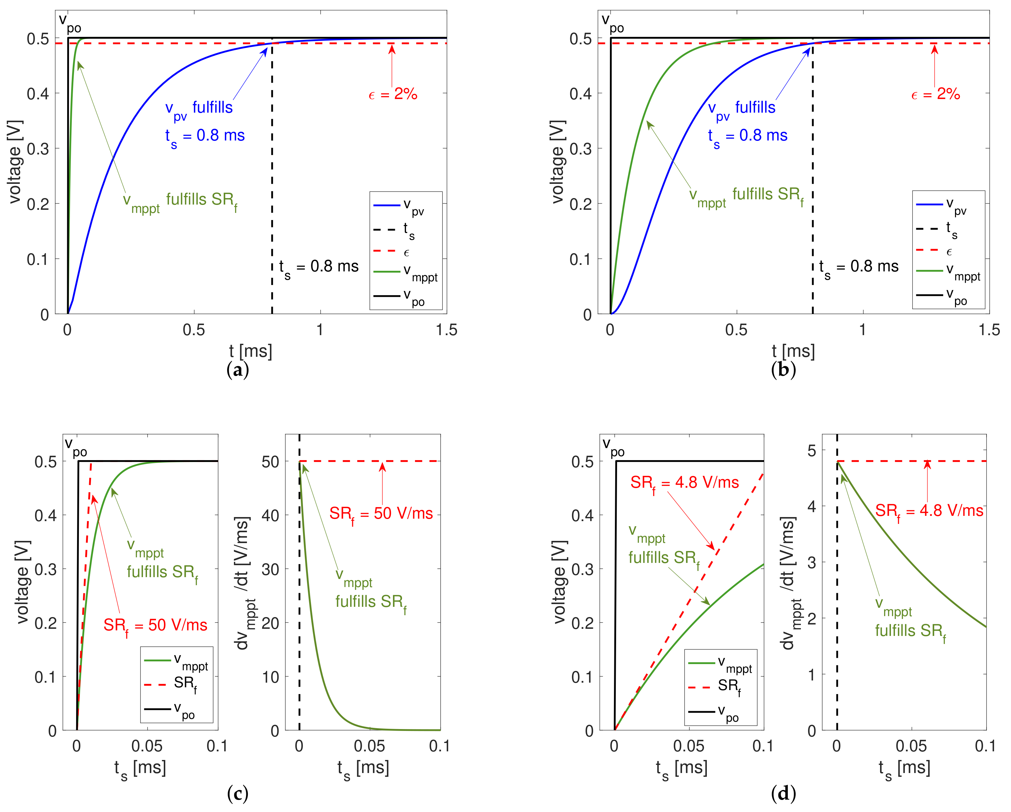
5.2. Reference Filter Design

Since the P & O reference v p o exhibits step changes with infinite derivatives, an additional block must be inserted into the MPPT block to limit the reference derivative, which is needed to ensure that both reachability conditions (24) and (26) are fulfilled. The block diagram of Figure 3 shows the internal structure of the MPPT block, which includes a filter to limit the derivative of the reference provided by the P&O algorithm ( v p o signal), thus providing a MPPT signal ( v m p p t ) with a derivative that ensures the global stability of the SMC.
This paper proposes a first-order filter to limit the maximum derivative of the MPPT reference v m p p t . Considering that positive and negative variations of the P&O signal v p o are steps and that the first-order filter provides the same output derivative for positive and negative inputs, the derivative of the MPPT reference will be the same for increments or decrements in the v p o signal. Therefore, the first step is to define the maximum filter derivative ( S R f ) that fulfills both S R p and S R n limits given in (24) and (26), which is calculated as follows:
S R f = max S R p , S R n
The transfer function G f of a first-order filter is reported in (32); such an expression also shows the Laplace representation of the v p o steps with amplitude Δ v p o and the Laplace calculation of the MPPT reference v m p p t .
G f = V m p p t ( s ) V p o ( s ) = Ω s + Ω V m p p t ( s ) = G f · Δ v p o s
Applying the inverse Laplace transformation leads to the time waveform of v m p p t ( t ) given in (33) and the time-derivative given in (34). The maximum value of d v m p p t d t ( t ) is obtained for t = 0 s , and such a maximum value must be set equal to S R f , which enables the calculation of the filter parameter Ω , as given in (35), to ensure a derivative of v m p p t lower than S R f for t > 0 .
v m p p t ( t ) = Δ v p o · 1 e Ω · t
d v m p p t d t ( t ) = Δ v p o · Ω · e Ω · t
Ω = S R f Δ v p o
Finally, designing the reference filter using (35) will ensure the SMC’s global stability.

5.3. Calculation of k 1

The calculation of the SMC parameter k 1 is performed using the closed-loop expression of v p v given in (30) and the v m p p t expression given in (32):
V p v ( s ) = k 1 C p v · s + k 1 · Ω s + Ω · Δ v p o s v m p p t
Applying the inverse Laplace transformation to (36) results in the following time-domain waveform of v p v :
v p v ( t ) = Δ v p o · 1 + Ω k 1 C p v Ω · e k 1 C p v · t k 1 C p v k 1 C p v Ω · e Ω · t
The previous closed-loop waveform of the PV voltage, as given in (37), shows that lim t v p v ( t ) = Δ v p o ; thus, the steady-state error is zero. In addition, parameter k 1 must be calculated to impose a desired settling time t s to the v p v waveform, which is measured when the PV voltage (37) reaches a given percentage of the final value Δ v p v , where the most common limit in engineering is ϵ = 2 % . Such a settling time must be less than the perturbation period T a of the P&O; otherwise, the P&O algorithm could become unstable, as demonstrated in [26,27]. Therefore, k 1 is calculated by solving (37) for v p v = Δ v p v · 1 ϵ and t = t s < T a to obtain the value given in (38), where W ( · ) is the Lambert-W function [28].
k 1 = 1 a 1 · W a 1 · e a 1 · ϵ a 2 a 2 ϵ a 2 ; a 1 = t s C p v , a 2 = ϵ + e Ω · t s Ω · C p v and t s < T a

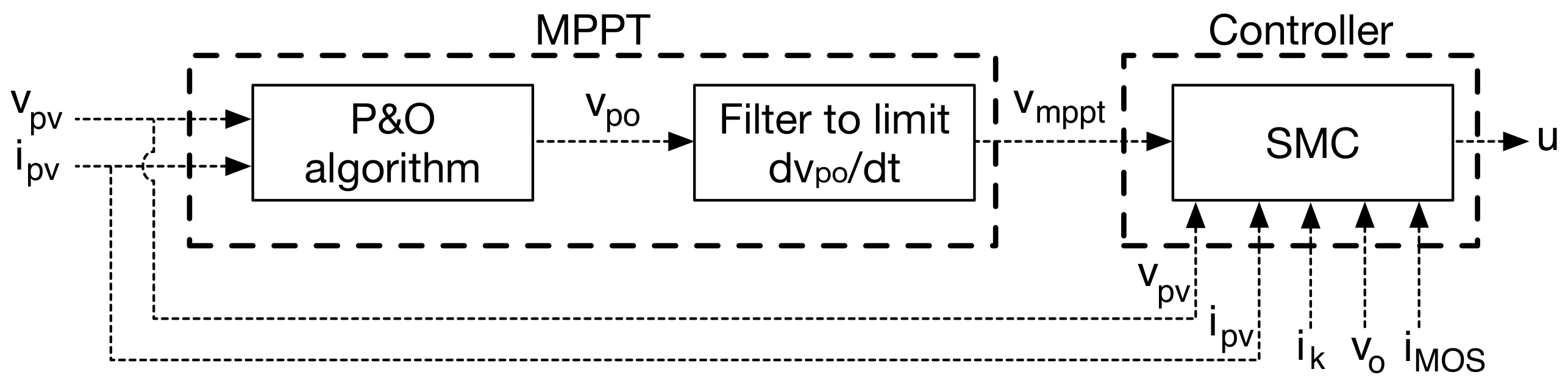
6. Implementation of the SMC and the MPPT Algorithm

The practical implementation of any SMC requires several steps:
  • Limit the switching frequency to avoid MOSFET saturation and reduce switching losses;
  • Derive a practical control law for the SMC;
  • Calculate both the switching function and the output signal in real-time.
Those topics are addressed in the following subsections.

6.1. Limiting the Switching Frequency

Theoretical sliding-mode controllers operate with infinite switching frequency [29]; hence, a widely adopted solution is to introduce a hysteresis band around the sliding surface, where the bandwidth defines the maximum switching frequency [30].
Figure 4 illustrates the hysteresis band effect on the switching frequency: the switching function derivative, given in (21), exhibits the derivatives imposed by the operating conditions; thus, increasing the width of the hysteresis band decreases the switching frequency because the switching function derivative will be a longer time in a given state (positive or negative).
Introducing a hysteresis band H , + H around the switching function ψ x (20) produces the practical sliding surface given below:
H < k 1 · v p v v m p p t + i p v k 2 · i m < + H
Taking into account that the design process provided in the previous sections ensures the global stability of the SMC, the average value of the PV voltage is equal to the MPPT reference, i.e., v p v = v m p p t . Similarly, the average value of the magnetizing current multiplied by the duty cycle is equal to the PV current, as given in (8), i.e., i m · d = i p v . On the other hand, both the PV voltage v p v and magnetizing current i m exhibit voltage δ v p v and current δ i m ripples, respectively, due to the switching action of the converter:
v p v = v p v + δ v p v i m = i m + δ i m
Therefore, the practical sliding surface defined in (39) can be rewritten as in (41), which considers the value k 2 = d , as previously defined in (29).
H < k 1 · δ v p v d · δ i m < + H
The ripples of the magnetizing current ( δ i m ) and PV voltage ( δ v p v ) are calculated from the switched Equations (1) and (2) using the flux-balance ( δ i m ) and charge balance ( δ v p v ), respectively. The δ i m value was calculated in the interval with u = 1 , with duration T s w · d , to use the shortest equation for the current derivative; similarly, the δ v p v value was calculated in the interval with u = 0 , with duration T s w · 1 d , which provides the shortest equation for the voltage derivative. The ripple expressions are reported as follows:
δ i m = v p v · d · T s w 2 · L m δ v p v = i p v · 1 d · T s w 2 · C p v
It is worth noting that the ripples defined in (42) can be used for a preliminary design of L m and C p v to obtain the desired values of δ i m and δ v p v , respectively. In that case, it would be necessary to define a given operating condition (i.e., irradiance and temperature) to determine v p v and i p v and define a given switching frequency and duty cycle in order to define T s w and d.
Substituting the previous expressions into (41) and considering the switching frequency F s w = 1 / T s w , the hysteresis limit H is calculated by (43) to ensure a maximum switching frequency F s w , where the duty cycle is calculated from (9) and depends on v p v , v o , L m , L k , and n.
H = 1 2 · F s w · k 1 · i p v · 1 d C p v v p v · d 2 L m
Finally, the maximum switching frequency is defined depending on the characteristics of the MOSFET and diode used for the construction of the flyback converter.

6.2. Control Law

The implementation of the practical sliding surface (39), which includes the hysteresis band H < ψ x < + H , requires the following control conditions:
  • Condition 1: u = 1 (MOSFET on, Diode off) imposes a negative switching function derivative d ψ x d t < 0 , as given in (14); hence, the switching function ψ x is decreasing. Moreover, from Figure 1, it is observed that u = 1 imposes i m = i M O S . When ψ x reaches the lower limit H , ψ x must increase to remain inside the hysteresis band. Therefore, the switching function derivative must be changed to a positive value d ψ x d t > 0 , which requires changing u = 0 according to (23).
  • Condition 0: u = 0 (MOSFET off, Diode on) imposes a positive d ψ x d t > 0 , as given in (14); hence, ψ x is increasing. Moreover, from Figure 1, it is observed that u = 0 imposes i m = n · i k . When ψ x reaches the upper limit + H , ψ x must be reduced to remain inside the hysteresis band; thus, the switching function derivative must be changed to a negative value d ψ x d t < 0 , which requires changing u = 1 according to (25).
The previous control behavior is formalized in the control law described below:
u = 0 if ψ x > + H with ψ x = k 1 · v p v v m p p t + i p v d · i M O S 1 if ψ x > H with ψ x = k 1 · v p v v m p p t + i p v d · n · i k
Such a control law is implemented using a hysteresis comparator, two adders, three subtractors, two multipliers, two gains, and a divider for the calculation of k 2 = d using (9). In addition, the MPPT filter can be implemented using an active filter based on the operational amplifiers. Figure 5 shows the block diagram for implementing the complete control system, including the MPPT block, the calculation of k 2 , the calculation of the switching function ψ x , and the hysteresis comparator that produces the MOSFET control signal u.

6.3. Summary of the Design Process

The design of both the SMC and MPPT first-order filter is based on the parameters defined for the P&O algorithm ( Δ v p v and T a ) and the maximum switching frequency ( F s w ). The design equations proposed in this paper for both the SMC and filter are summarized as follows:
1
The derivative limits of the MPPT reference ( S R p and S R n ) are calculated from (24) and (26) using k 1 ;
2
The filter derivative S R f is calculated from S R p and S R n using (31);
3
The value of Ω is calculated from S R f and Δ v p v using (35);
4
The value of k 1 is calculated from Ω and t s with (38);
5
The value of H is calculated from F s w and k 1 with (43).
The previous summary shows that steps 1, 2, 3, and 4 depend on each other; therefore, the simultaneous equation system formed by (24), (26), (31), (35) and (38) must be solved. Finally, the parameter H is calculated using (43). The following section illustrates this design process using a practical application example.

7. Design Example and Simulation Results

This section presents an application example to illustrate the design process of the proposed SMC under realistic conditions. Table 1 reports the electrical parameters adopted for the PV system in Figure 1, where the PV panel is a BP585 [11] and the transformer of the flyback converter is a Nascent 95073 [31]. Finally, the output voltage of the flyback converter is set to 220 V, which is within the voltage range adopted for single-phase microinverters based on full-bridge inverters in the second stage connected to a 110 V grid [6,7].

7.1. Numerical Analysis and Design

The parameters of the P&O algorithm, as reported in Table 1, were calculated following the procedures validated in [26,27], which are the starting point for the design procedure summarized in Section 6.3. Then, solving the simultaneous equation system formed by (24), (26), (31), (35) and (38) for a settling time lower than T a ( t s < 1.0 ms) results in the feasible k 1 and Ω values reported in Figure 6a, where the maximum Ω value is 725 krad/s, while the maximum value of k 1 is 11 A/V (out of the figure). The numerical analysis shows that high k 1 values reduce the settling time of the PV voltage, while high Ω values (i.e., Ω > 80 krad/s) do not affect, significantly, such a settling time. Figure 6a reports a first option for the SMC and filter parameters ( k 1 and Ω ) to regulate the application example of this section. This first option, named Option 1, is characterized by Ω = 100 krad/s and k 1 = 0.49 A/V, which ensures a settling time t s = 0.8 ms < 1 ms, where t s = 0.8 ms was selected to provide a 20 % safe margin under the perturbation period T a = 1 ms.
The left side of Figure 6a shows that low values of Ω have an impact on both the settling time and k 1 values; hence, Figure 6b shows a zoom for 4 krad/s Ω 10 krad/s, which confirms the impact of Ω on those qualities. In fact, such a figure shows that the same settling time is achievable with two couples of k 1 and Ω values, where increments in k 1 allow the reduction in Ω for the same t s value. For example, Figure 6b reports a second option for the SMC and filter parameters, named Option 2, which is characterized by Ω = 9.6 krad/s and k 1 = 0.61 A/V, which ensures the same settling time of Option 1 ( t s = 0.8 ms). It is remarkable that reducing Ω by 10.4 times only requires multiplying k 1 by 1.24 to obtain the same settling time with global stability. This condition is confirmed by the time responses depicted in Figure 7, where Figure 7a shows the time response of Option 1 (high Ω ) and Figure 7b shows the time response of Option 2 (low Ω ).
The time response of Option 1 (high Ω ) shows that the PV voltage fulfills the desired t s = 0.8 ms. However, even though the derivative of v m p p t fulfills the stability restriction, the high-value of Ω imposes a fast rise in v m p p t , and thus, a high voltage slew-rate ( S R f = 50 V/ms) is needed. The time response of Option 2 (low Ω ) shows that the PV voltage also ensures the desired t s = 0.8 ms, but the low value of Ω imposes a slow rise in v m p p t ; thus, a low voltage slew-rate ( S R f = 4.8 V/ms) is needed, and a cheaper operational amplifier can be used to implement the reference filter in comparison to Option 1. Such a slew-rate difference is confirmed in Figure 7c,d, which shows the maximum slew-rate acceptable and the waveform of v m p p t , and in both cases, S R f is fulfilled, but Option 1 exhibits a much higher voltage derivative.
Considering that both Option 1 and Option 2 produce the same PV voltage, but Option 2 requires a slower (and cheaper) hardware for the filter implementation, this example adopts Option 2: Ω = 9.6 krad/s, k 1 = 0.61 A/V, t s = 0.8 ms. In general, the solution with a lower Ω is desirable since a less restrictive slew rate is needed. Finally, the flyback converter will be constructed with a MOSFET and a diode supporting 100 kHz, which requires a hysteresis band with a peak amplitude lower than 0.47 A according to the design equation given in (43). Then, the hysteresis parameter is set to H = 0.5 A to provide a safe margin, which ensures a switching frequency lower than 95 kHz.
Using detailed circuital simulations, the following subsection validated the SMC and filter performance considering the selected parameters.

7.2. Circuital Simulations

The validation of the flyback-based PV system and the designed SMC is performed using detailed circuital simulations implemented in the power electronics simulator PSIM [32]. The PSIM environment allows the implementation of the power circuit described in Figure 1 using accurate models for each element (MOSFET, diode, transformer, etc.), and the control circuit reported in Figure 5 was implemented using adders, gains, comparators, and other non-linear circuits. Finally, the P&O circuit was implemented using a C-block, which enables the introduction of a C-code, with the P&O algorithm, into the PSIM simulation, thus emulating the classical P&O implementation based on microcontrollers programmed with the same C-code. Figure 8 shows the PSIM implementation of both the power circuit and the control system.
Figure 9 shows the results of the circuital simulations performed in PSIM, where the P&O algorithm provides step changes using the signal v p o . Two different PSIM simulations were conducted, where the first one considers a high irradiance ( S = 1000 W/m 2 ) reaching the PV panel, and the second one considers a low irradiance ( S = 200 W/m 2 ) condition; moreover, both conditions assume a PV module temperature of 25 °C (T = 25 °C). Thus, the PV system is tested under the extreme conditions considered in the design process. In this way, Figure 9a shows the PV voltage v p v waveform, which has the same dynamic response as the theoretical signal generated with Equation (37) and previously tested in Figure 7. Therefore, the circuital response of the PV voltage has the desired settling time t s = 0.8 ms for high-irradiance conditions, as is observed in Figure 9a. Similarly, Figure 9b shows the PV voltage v p v waveform for a low-irradiance condition, which describes the same dynamic response and settling-time, where the only difference is the smaller switching ripple, which is predicted by Equation (42), due to the lower PV current. In conclusion, the proposed SMC ensures the desired PV voltage response in any irradiance condition, which ensures the correct operation of the P&O algorithm.
Figure 9c,d confirms the correct operation of the SMC: the switching function ψ x defined in (44) produces the correct control signal u, which ensures that ψ x is always trapped inside the hysteresis band ( H < ψ x < + H ) and that both reachability and equivalent control conditions are fulfilled. Therefore, Figure 9c,d confirms that the SMC provides global stability for any irradiance condition.
Figure 10a shows the I–V and P–V curves of the BP585 PV panel adopted for this application example, where the MPP conditions are the following considering T = 25 °C:
  • S = 1000 W/m 2 : the MPP voltage is 18.4 V, the MPP current is 4.63 A, and the MPP power is 85 W.
  • S = 600 W/m 2 : the MPP voltage is 17.7 V, the MPP current is 2.77 A, and the MPP power is 49 W.
  • S = 200 W/m 2 : the MPP voltage is 16.2 V, the MPP current is 0.92 A, and the MPP power is 15 W.
A correct operation of the PV system under the previous irradiance values must reach those MPP conditions. Therefore, the system was tested under variable irradiance conditions to confirm the correct operation of the SMC and P&O algorithm. In this way, Figure 10b shows the simulation of the PV system operating at 1000 W/m 2 up to 13 ms, and at that time, the irradiance changes suddenly to 200 W/m 2 . Moreover, this simulation also considers a 35 % peak-to-peak perturbation in the output voltage v o , which is caused by the inverter operation at the second stage of a PV microinverter. The simulation confirms the correct operation of both the P&O algorithm and SMC since the PV power p p v is always at the MPP voltage for both irradiance conditions, except for the small time-interval between 13 ms and 18 ms, which is the time (5 ms) required by the P&O to track the new MPP condition. After the new MPP condition is reached, the PV voltage describes the stable three-point behavior of the P&O, which confirms the stable operation of the PV system.
Figure 10b also reports the duty cycle of the flyback converter, which is never saturated, and thus, the PV system is stable. This is expected since the simulations in Figure 9 confirm that the reachability conditions are fulfilled; hence, the equivalent control condition 0 < u e q = d < 1 is also fulfilled. Moreover, the duty cycle waveform confirms the global stability of the PV system even with perturbations on both the irradiance and the output voltage. Finally, the simulation also reports the switching frequency of the flyback converter, which is always below the designed maximum value (95 kHz). In conclusion, the circuital simulations presented in this section confirm the stability of the SMC under realistic conditions, which ensures that the P&O algorithm is able to track the optimal operating conditions of the PV panel (reference variations) even under varying irradiance levels (line variations) and with voltage oscillations at the output port (load varions), which are frequently caused by the inverter connection inside the microinverter.

8. Conclusions

An integrated design procedure for the sliding-mode control of the first-stage flyback that belongs to a PV system was presented and validated in this paper. The first stage of the microinverter was modeled through the differential equations of the state variables and the averaged model. In this case, specific attention was put on the SMC design; therefore, the basic concepts of the sliding-mode controller applied to power converters were presented. The establishment of the sliding surface was briefly but clearly presented to contribute to the application of the SMC approach. The transversality, reachability, and equivalent control tests were presented in detail with the same objective. Because the power extraction had to be implemented with a maximum power point tracking algorithm, the MPPT output was filtered to limit its derivative. This action was developed to achieve the reachability test, integrating the filter parameter estimation into the design procedure. The integrated design was presented as a list of steps and then validated in an application example. First, the PV module parameters, the flyback converter parameters, the perturbation amplitude and the perturbation period of the P&O algorithm, and the maximum switching frequency were presented. Then, a simultaneous equation system was solved to obtain the necessary SMC and MPPT parameters to achieve a specific error of the P&O voltage and a specific stabilization time. A circuital simulation of the PV system was carried out, and the simulation results showed that following the integrated design procedure, it is possible to obtain an SMC and an MPPT to control the flyback converter in a microinverter to connect PV modules with AC loads or even with the AC grid.

Author Contributions

Conceptualization, C.A.R.-P., A.J.S.-M. and J.D.B.-R.; methodology, C.A.R.-P., A.J.S.-M. and J.D.B.-R.; software, C.A.R.-P., A.J.S.-M. and J.D.B.-R.; validation, C.A.R.-P., A.J.S.-M. and J.D.B.-R.; writing—original draft preparation, C.A.R.-P., A.J.S.-M. and J.D.B.-R.; writing—review and editing, C.A.R.-P., A.J.S.-M. and J.D.B.-R. All authors have read and agreed to the published version of the manuscript.

Funding

This research and the APC were funded by Minciencias, Universidad Nacional de Colombia, Universidad del Valle, and Instituto Tecnológico Metropolitano under the research project “Dimensionamiento, planeación y control de sistemas eléctricos basados en fuentes renovables no convencionales, sistemas de almacenamiento y pilas de combustible para incrementar el acceso y la seguridad energética de poblaciones colombianas”, (Minciencias code 70386), which belongs to the research program “Estrategias para el desarrollo de sistemas energéticos sostenibles, confiables, eficientes y accesibles para el futuro de Colombia”, (Minciencias code 1150-852-70378, Hermes code 46771).

Institutional Review Board Statement

Not applicable.

Informed Consent Statement

Not applicable.

Data Availability Statement

The data used in this study are reported in the paper’s figures and tables.

Acknowledgments

The authors thank the Facultad de Minas (Sede Medellin) and Facultad de Ingeniería y Arquitectura (Sede Manizales) of the Universidad Nacional de Colombia.

Conflicts of Interest

The authors declare no conflict of interest.

References

  1. IEA. Snapshot of Global PV Markets 2021; Technical Report; International Energy Agency: Rheine, Germany, 2021. [Google Scholar]
  2. Petrone, G.; Ramos-Paja, C.A.; Spagnuolo, G. Photovoltaic Sources Modeling; John Wiley & Sons Ltd.: Chichester, UK, 2017. [Google Scholar] [CrossRef]
  3. Mehedi, I.M.; Salam, Z.; Ramli, M.Z.; Chin, V.J.; Bassi, H.; Rawa, M.J.; Abdullah, M.P. Critical evaluation and review of partial shading mitigation methods for grid-connected PV system using hardware solutions: The module-level and array-level approaches. Renew. Sustain. Energy Rev. 2021, 146, 111138. [Google Scholar] [CrossRef]
  4. Çelik, Ö.; Teke, A.; Tan, A. Overview of micro-inverters as a challenging technology in photovoltaic applications. Renew. Sustain. Energy Rev. 2018, 82, 3191–3206. [Google Scholar] [CrossRef]
  5. Enphase. 2021. Comparing Inverters: Make the Smartest Choice in Solar. Available online: https://www4.enphase.com/en-au/products-and-services/microinverters/vs-string-inverter (accessed on 26 November 2021).
  6. Microchip. Grid-Connected Solar Microinverter Reference Design Using a dsPIC® Digital Signal Controller-AN1338; Technical Report; Microchip: Chandler, AZ, USA, 2011. [Google Scholar]
  7. Manoharan, M.S.; Ahmed, A.; Seo, J.W.; Park, J.H. Power conditioning for a small-scale PV system with charge-balancing integrated micro-inverter. J. Power Electron. 2015, 15, 1318–1328. [Google Scholar] [CrossRef] [Green Version]
  8. Ahmed, M.E.S.; Orabi, M.; AbdelRahim, O.M. Two-stage micro-grid inverter with high-voltage gain for photovoltaic applications. IET Power Electron. 2013, 6, 1812–1821. [Google Scholar] [CrossRef]
  9. Trujillo, C.L.; Santamaría, F.; Gaona, E.E. Modeling and testing of two-stage grid-connected photovoltaic micro-inverters. Renew. Energy 2016, 99, 533–542. [Google Scholar] [CrossRef]
  10. Evran, F. Plug-in repetitive control of single-phase grid-connected inverter for AC module applications. IET Power Electron. 2017, 10, 47–58. [Google Scholar] [CrossRef]
  11. BP Solar. 2003. Datasheet BP 585. Available online: https://atlantasolar.com/pdf/BPSolar/BP585U.pdf (accessed on 26 November 2021).
  12. Trina Solar. Residential Module: Multi-Busbar Mono PERC Module. 2020. Available online: https://static.trinasolar.com/sites/default/files/Datasheet_DE06\X.05%28II%29_NA_2021_A.pdf (accessed on 26 November 2021).
  13. Garcerá, G.; González-Medina, R.; Figueres, E.; Sandia, J. Dynamic modeling of DC—DC converters with peak current control in double-stage photovoltaic grid-connected inverters. Int. J. Circuit Theory Appl. 2012, 40, 793–813. [Google Scholar] [CrossRef] [Green Version]
  14. Bagheri, F.; Guler, N.; Komurcugil, H. Sliding Mode Current Observer for a Bidirectional Dual Active Bridge Converter. In Proceedings of the IECON 2021—47th Annual Conference of the IEEE Industrial Electronics Society, Toronto, ON, Canada, 13–16 October 2021; pp. 1–6. [Google Scholar] [CrossRef]
  15. Jayalaksmi, N.S.; Gaonkar, D.N.; Naik, A. Design and analysis of dual output flyback converter for standalone PV/battery system. Int. J. Renew. Energy Res. 2017, 7, 1032–1040. [Google Scholar]
  16. Feng, J.; Wang, H.; Xu, J.; Su, M.; Gui, W.; Li, X. A Three-Phase Grid-Connected Microinverter for AC Photovoltaic Module Applications. IEEE Trans. Power Electron. 2018, 33, 7721–7732. [Google Scholar] [CrossRef]
  17. Raj, P.J.; Prabhu, V.V.; Premkumar, K. Fuzzy Logic-based Battery Management System for Solar-Powered Li-Ion Battery in Electric Vehicle Applications. J. Circuits Syst. Comput. 2021, 30, 2150043. [Google Scholar] [CrossRef]
  18. Dhiman, S.; Nijhawan, P. An improved PV system with auto-protection to inject active power into the power grid of marine ships. Indian J. Geo-Mar. Sci. 2020, 49, 1132–1142. [Google Scholar]
  19. Lopes Filho, G.; Franco, R.A.P.; Vieira, F.H.T. Maximum Power Point Tracking for Photovoltaic Panels Using Model Predictive Control and Incremental Conductance. Electr. Power Components Syst. 2021, 49, 345–360. [Google Scholar] [CrossRef]
  20. Dhiman, S.; Nijhawan, P. Design & analysis of improved bus-tied photovoltaic system for marine ships. Indian J. Geo-Mar. Sci. 2019, 48, 1963–1970. [Google Scholar]
  21. Loukriz, A.; Haddadi, M.; Messalti, S. Simulation and experimental design of a new advanced variable step size Incremental Conductance MPPT algorithm for PV systems. ISA Trans. 2016, 62, 30–38. [Google Scholar] [CrossRef]
  22. Messalti, S.; Harrag, A.; Loukriz, A. A new variable step size neural networks MPPT controller: Review, simulation and hardware implementation. Renew. Sustain. Energy Rev. 2017, 68, 221–233. [Google Scholar] [CrossRef]
  23. Komurcugil, H.; Biricik, S.; Bayhan, S.; Zhang, Z. Sliding Mode Control: Overview of Its Applications in Power Converters. IEEE Ind. Electron. Mag. 2021, 15, 40–49. [Google Scholar] [CrossRef]
  24. Babes, B.; Mekhilef, S.; Boutaghane, A.; Rahmani, L. Fuzzy Approximation-Based Fractional-Order Nonsingular Terminal Sliding Mode Controller for DC-DC Buck Converters. IEEE Trans. Power Electron. 2022, 37, 2749–2760. [Google Scholar] [CrossRef]
  25. Liu, J.; Laghrouche, S.; Harmouche, M.; Wack, M. Adaptive-gain second-order sliding mode observer design for switching power converters. Control. Eng. Pract. 2014, 30, 124–131. [Google Scholar] [CrossRef] [Green Version]
  26. Femia, N.; Petrone, G.; Spagnuolo, G.; Vitelli, M. Optimization of Perturb and Observe Maximum Power Point Tracking Method. IEEE Trans. Power Electron. 2005, 20, 963–973. [Google Scholar] [CrossRef]
  27. Femia, N.; Petrone, G.; Spagnuolo, G.; Vitelli, M. A technique for improving P&O MPPT performances of double-stage grid-connected photovoltaic systems. IEEE Trans. Ind. Electron. 2009, 56, 4473–4482. [Google Scholar] [CrossRef]
  28. Corless, R.M.; Gonnet, G.H.; Hare, D.E.G.; Jeffrey, D.J.; Knuth, D.E. On the LambertW function. Adv. Comput. Math. 1996, 5, 329–359. [Google Scholar] [CrossRef]
  29. Tan, S.C.; Lai, Y.M.; Tse, C.K. Sliding Mode Control of Switching Power Converters; CRC Press: Boca Raton, FL, USA, 2011; p. 368. [Google Scholar] [CrossRef]
  30. González Montoya, D.; Ramos-Paja, C.A.; Giral, R. Improved Design of Sliding-Mode Controllers Based on the Requirements of MPPT Techniques. IEEE Trans. Power Electron. 2016, 31, 235–247. [Google Scholar] [CrossRef] [Green Version]
  31. NASCENTechnology. LTCC High Voltage Flyback Transformer 95073, 95073-STX; NASCENTechnology Inc.: Watertown, SD, USA, 2013. [Google Scholar]
  32. PSIM. PSIM: The Ultimate Simulation Environment for Power Conversion and Motor Control; PSIM: Rockville, MD, USA, 2021; Available online: https://powersimtech.com/products/psim/capabilities-applications/ (accessed on 26 November 2021).
Figure 1. Electrical model of a flyback-based PV system as first the stage of a microinverter.
Applsci 12 01399 g001
Figure 2. P&O algorithm: flowchart, behavior, and waveforms.
Applsci 12 01399 g002
Figure 3. Block diagram of the MPPT block.
Applsci 12 01399 g003
Figure 4. Practical sliding surface for limited switching frequency.
Applsci 12 01399 g004
Figure 5. Implementation of the proposed control system.
Applsci 12 01399 g005
Figure 6. k 1 and Ω calculation to fulfill t s and S R f restrictions. (a) k 1 and Ω feasible values for t s < 1 ms. (b) k 1 feasible values with low Ω .
Applsci 12 01399 g006
Figure 7. Time response and v m p p t derivative of Option 1 (high Ω ) and Option 2 (low Ω ). (a) Time response of Option 1 (high Ω ): Ω = 100 krad/s, k 1 = 0.49 A/V, t s = 0.8 ms. (b) Time response of Option 2 (low Ω ): Ω = 9.6 krad/s, k 1 = 0.61 A/V, t s = 0.8 ms. (c) Option 1 (high Ω ) fulfills the v m p p t derivative restrictions for global stability. (d) Option 2 (low Ω ) fulfills the v m p p t derivative restrictions for global stability.
Applsci 12 01399 g007
Figure 8. Circuital scheme implemented in PSIM.
Applsci 12 01399 g008
Figure 9. Circuital simulation of the PV system. (a) PV voltage response at high irradiance (1000 W/m 2 ). (b) PV voltage response at low irradiance (200 W/m 2 ). (c) Switching function and control law at high irradiance (1000 W/m 2 ). (d) Switching function and control law at low irradiance (200 W/m 2 ).
Applsci 12 01399 g009
Figure 10. SMC and MPPT performance for variations on both the irradiance and output voltage. (a) I–V and P–V curves of the BP585 panel at 1000 W/m 2 , 600 W/m 2 , and 200 W/m 2 . (b) Circuit response to simultaneous perturbations.
Applsci 12 01399 g010
Table 1. Parameters for the design example.
PV Panel
    MPP voltage ( v m p p )18.5 V
    MPP power ( p m p p )85.5 W
    Short-circuit current ( i s C )5.0 A
    Open-circuit voltage ( v o C )22.1 V
Flyback Converter
    Input capacitor ( C p v ) 100 μ F
    Magnetizing inductor ( L m ) 75 μ H
    Leakage inductor ( L k ) 11 μ H
    Turn-ratio (n) 8.0
    Average output voltage ( v o )220 V
P&O Algorithm
    Perturbation amplitude ( Δ v p v )0.5 V
    Perturbation period ( T a )1 ms
Publisher’s Note: MDPI stays neutral with regard to jurisdictional claims in published maps and institutional affiliations.

