Communication

High-Q TeO2–Si Hybrid Microring Resonators

by
Khadijeh Miarabbas Kiani
*,
Dawson B. Bonneville
,
Andrew P. Knights
and
Jonathan D. B. Bradley
Department of Engineering Physics, McMaster University, 1280 Main Street West, Hamilton, ON L8S 4L7, Canada
*
Author to whom correspondence should be addressed.
Appl. Sci. 2022, 12(3), 1363; https://doi.org/10.3390/app12031363
Submission received: 12 January 2022 / Revised: 25 January 2022 / Accepted: 25 January 2022 / Published: 27 January 2022

Abstract

:
We present the design and experimental measurement of tellurium oxide-clad silicon microring resonators with internal Q factors of up to 1.5 × 10⁶, corresponding to a propagation loss of 0.42 dB/cm at wavelengths around 1550 nm. This compares to a propagation loss of 3.4 dB/cm for unclad waveguides and 0.97 dB/cm for waveguides clad with SiO2. We compared our experimental results with the Payne–Lacey model describing propagation dominated by sidewall scattering. We conclude that the relative increase in the refractive index of TeO2 reduces scattering sufficiently to account for the low propagation loss. These results, in combination with the promising optical properties of TeO2, provide a further step towards realizing compact, monolithic, and low-loss passive, nonlinear, and rare-earth-doped active integrated photonic devices on a silicon photonic platform.

1. Introduction

The impact of silicon photonics on the development of photonic integrated circuits (PICs) is considerable, because of device compatibility with complementary metal–oxide–semiconductor (CMOS) technology and the leveraging of decades of research stimulated by the microelectronics industry [1]. The miniaturization of photonic waveguides has emerged as one of the most prominent technology platforms for PICs in recent decades [2].
The reduction in propagation loss associated with silicon waveguides is an ongoing research area because loss is a key parameter for link budget management in on-chip optical networks and many important micro-photonic devices, as well as passive and active systems including sensors, filters, delay lines, and light sources [3,4,5,6]. One device structure for which propagation loss is particularly critical is the microring resonator (MRR). MRRs provide an efficient cavity which has a compact size, wavelength selectivity, tunability, scalability, and functional versatility [7], making them a prominent candidate for a variety of applications including lasers [8,9], optical sensors [10], nonlinear optics [11,12], quantum optics [13], (de-)multiplexing systems [14], optical filters [15], and optical modulators [16]. The loss in MRRs can be quantified by the cavity Q factor, which is typically limited to values on the order of 105 in standard 220 nm-high single-mode silicon MRRs around 1550 nm.
Several approaches have been explored for enhancing the Q factor in silicon MRRs, including minimizing light scattering at roughened sidewalls via shallow-etched or multi-mode waveguide designs and alternative fabrication methods based on selective oxidation, e-beam lithography, reactive ion plasma etching, inductively coupled plasma (ICP) etching, or low-pressure chemical vapor deposition (LPCVD). High-Q factor silicon MRRs fabricated using a selective oxidation process have been shown with intrinsic Q factors of 5.1 × 10⁵ [17] and 7.6 × 10⁵ [18], although challenges remain in the control of the fabrication process [19]. A silicon microring resonator with a Q factor of 1.7 × 10⁶ was demonstrated using a large cross-section multi-mode waveguide with a severely limited free spectral range (FSR) of 17.1 pm [20]. With a similar approach, a silicon microring resonator with a high Q of 1.3 × 10⁶ and larger FSR was proposed in [21], with a bend radius of 450 μm. A silicon MRR with an internal Q factor of 1.1 × 10⁶ and FSR of 0.208 nm and utilizing a multi-mode ridge waveguide was fabricated using a standard CMOS-compatible silicon-on-insulator (SOI) process [22]. A multi-mode ultrahigh quality factor racetrack resonator with a 1.6 µm width was proposed using a standard single-etching process with a quality factor of 2.3 × 10⁶ provided by a multi-project wafer foundry [23]. An internal quality factor of 2.2 × 10⁷, corresponding to a 2.7 dB/m propagation loss, was achieved in a silicon microring resonator with a radius of 2.45 mm cladded with silicon oxide [24] by oxidizing the wafer surface in a steam oxidation process and using a reflowing photoresist strategy. An intrinsic Q factor of 1.57 × 10⁶, corresponding to a waveguide loss of 0.35 dB/cm, was realized in a silicon MRR with a radius of 150 μm and an FSR of 0.845 nm using e-beam lithography with a top cladding of a glass-like compound from hydrogen silsequioxane (HSQ) covered with a silicon oxide layer [25]. Low-loss submicron silicon-on-insulator strip waveguides were reported with a 0.5 dB/cm loss at 1310 nm and a 30 μm bend radius, cladded with silicon oxide [26] using H2 plasma post-lithography treatment and H2 thermal annealing after silicon etching. More generally, propagation losses lower than 0.4 dB/cm for the C-band and 0.8 dB/cm for the O-band of silicon wire waveguides have been reported for waveguides with a 440 nm core width, 220 nm core height, and 2 μm-thick SiO2 cladding layer defined by a high-resolution immersion lithography process [27]. While all of these approaches to improving Q factors in silicon MRRs are promising for different applications, they either suffer from performance trade-offs (e.g., multi-mode operation, larger footprint, and/or significantly reduced FSR) or add fabrication cost and complexity.
In this paper, we demonstrate a silicon MRR with a Q factor of 1.5 × 10⁶ at 1550 nm, corresponding to a propagation loss of 0.42 dB/cm, fabricated with a standard foundry process, plus a low-temperature post-process deposition of a TeO2 cladding layer. In addition to enabling a straightforward and monolithic low-loss hybrid waveguide structure, TeO2 has promising optical properties for new functionalities in silicon photonic microsystems. TeO2 has been shown to be thermally and chemically stable, possess high nonlinearity, and low optical attenuation from visible to mid-infrared wavelengths (0.4~5 µm), and have a high refractive index (2.1 at 1550 nm) and low dispersion [28]. Furthermore, the unique site variability in the TeO2 glass matrix enables high rare-earth dopant solubility and leads to large emission bandwidths, motivating its application in integrated optical amplifiers and lasers [29,30,31], including the recent demonstration of a hybrid rare-earth laser directly on silicon with an internal quality factor of 5.6 × 10⁵ [32]. This low-loss platform has significant potential for linear, nonlinear, and active optical applications in silicon photonics.

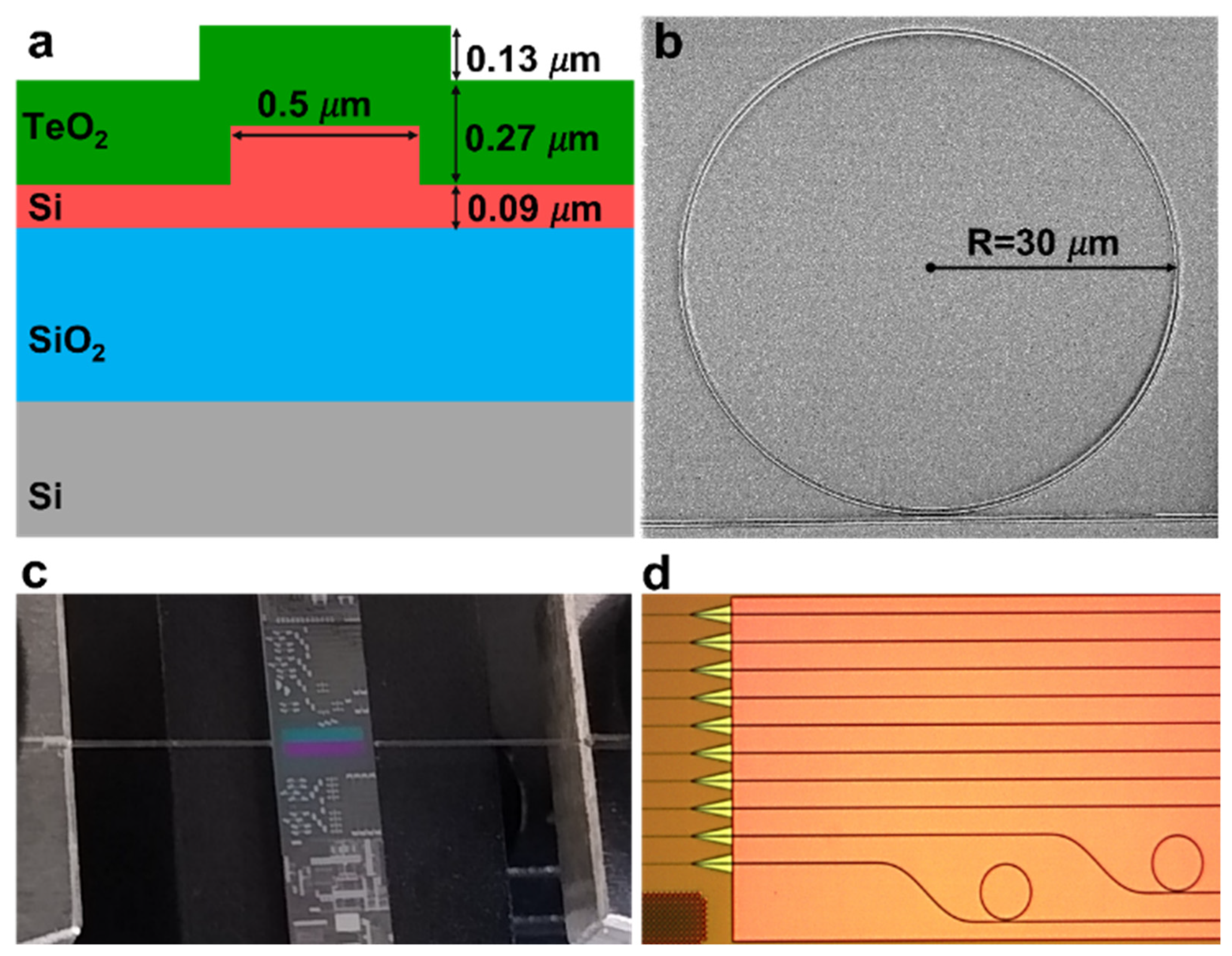
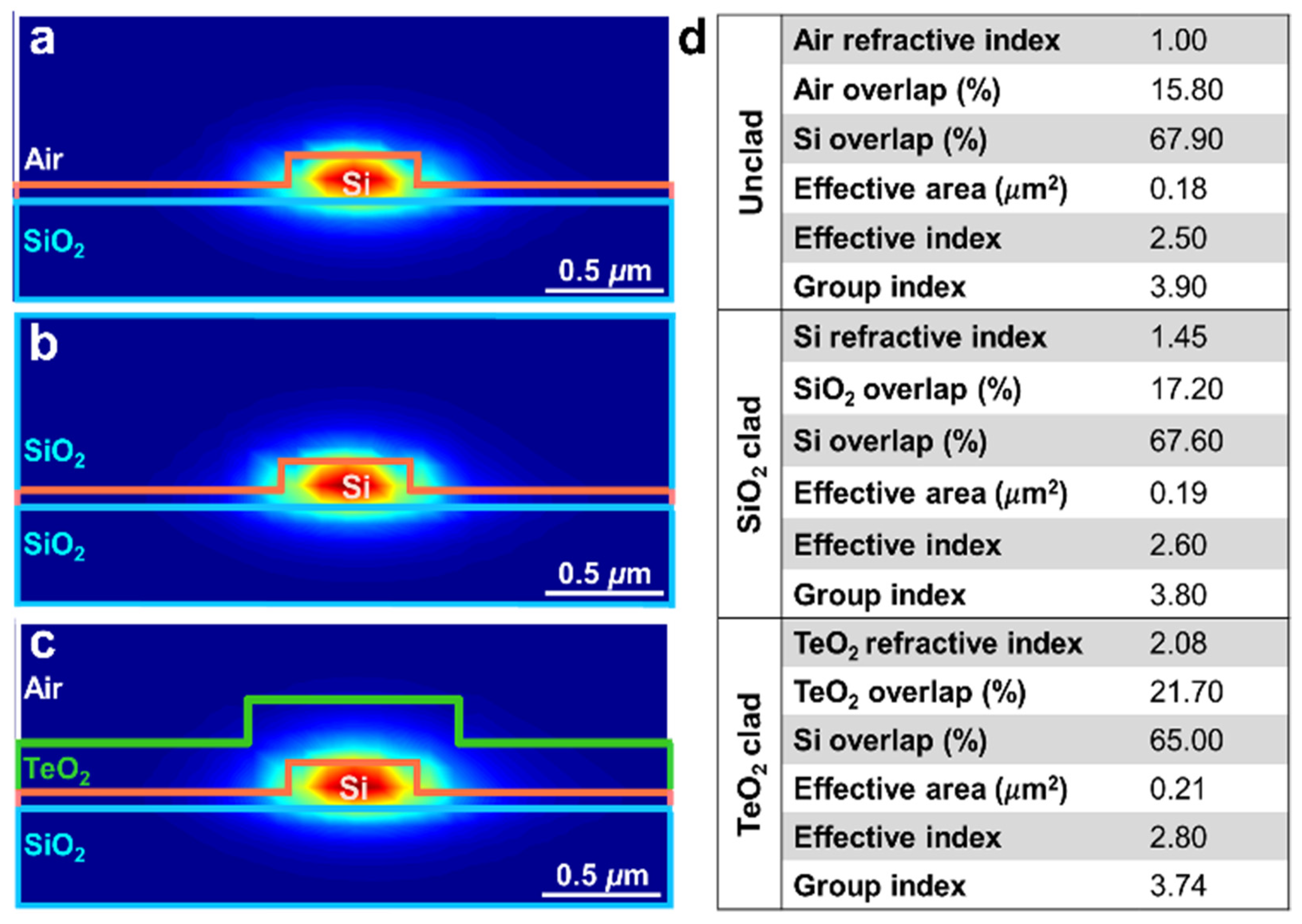
2. Microring Resonator Fabrication and Design

The microring resonator structure used in this work is displayed in Figure 1. It consists of an integrated silicon microring and bus waveguide coated with a thin film of tellurium oxide (TeO2). The silicon structure was fabricated in a silicon photonics foundry on a wafer-scale SOI platform with a 220 nm silicon layer thickness and consists of a 30 µm-radius silicon microring constructed using a 0.5 µm-wide waveguide. The bus waveguide is 0.4 µm wide, and the point coupling gap is 1.0 µm. The structure was cladded with SiO2, and subsequently, a window on top of the microring resonator was etched to the silicon layer for use in the post-processing TeO2 deposition or unclad device experiments. A set of devices with identical dimensions but without the SiO2 cladding etched was also fabricated for comparison. Deep etching was used for end-facet preparation and wafer dicing. For the TeO2-clad devices, the structure was coated with a 270 nm-thick TeO2 film deposited using a room-temperature reactive RF co-sputtering post-processing step with 145 W of tellurium target sputtering power, 2.8 mTorr chamber pressure, and 12 and 7.6 sccm of argon and oxygen flow, respectively. The substrate temperature was set at 20 °C. A top-view scanning electron microscope (SEM) image and the cross-section diagram of the TeO2-coated Si microring resonator are displayed in Figure 1a,b, respectively. Figure 1c,d show the image of the experimental setup and a microscopic image of the microring resonator with an open window structure.
The electric field profiles of the transverse-electric (TE)-polarized fundamental modes calculated using a finite element method (FEM) modesolver for the (cladding–core) TeO2–Si, SiO2–Si, and air–Si waveguides at a 1550 nm wavelength are displayed in Figure 2a–c, respectively. We also summarize the calculated optical properties of the TeO2–Si, SiO2–Si, and air–Si microring resonator structures in Figure 2d. The microring resonators and the bus waveguides were designed to achieve single-mode waveguide conditions at 1.55 to 2 μm wavelengths. The ring waveguide structure supports the TE-polarized and TM-polarized modes, and it has a low bending radiation loss at 1550 nm for TE only. The effective index of the TeO2-coated resonator is 2.8, which is almost 7.7 and 12% higher than that of the air- and SiO2-clad devices. For the TeO2-coated Si microring resonator, 21.7% of the optical power is confined in the TeO2 coating layer, while 65.0% is confined in the silicon layer. The rest of the optical power is confined in the lower SiO2 cladding. Slightly lower cladding confinement of 15.8 and 17.2%, respectively, is observed in the air- and SiO2-clad cases. The effective area is slightly larger in the TeO2-coated Si microring resonator than SiO2-coated and uncoated silicon microring resonators, although the mode is pulled upward more into the cladding, both of which can influence the ring–bus waveguide coupling.
The TeO2-coated resonator has a higher mode area of approximately 0.20 μm2 at 1.55 μm. The effective index increases for the TeO2 film cladding as the resonant mode becomes more confined in the TeO2 layer. The expansion of the optical mode at longer wavelengths decreases the effective index. The results show that approximately 60% of the mode power is confined in the Si region and 26% in the TeO2-cladded layer for the TeO2 cladding at a wavelength of 1.55 μm.

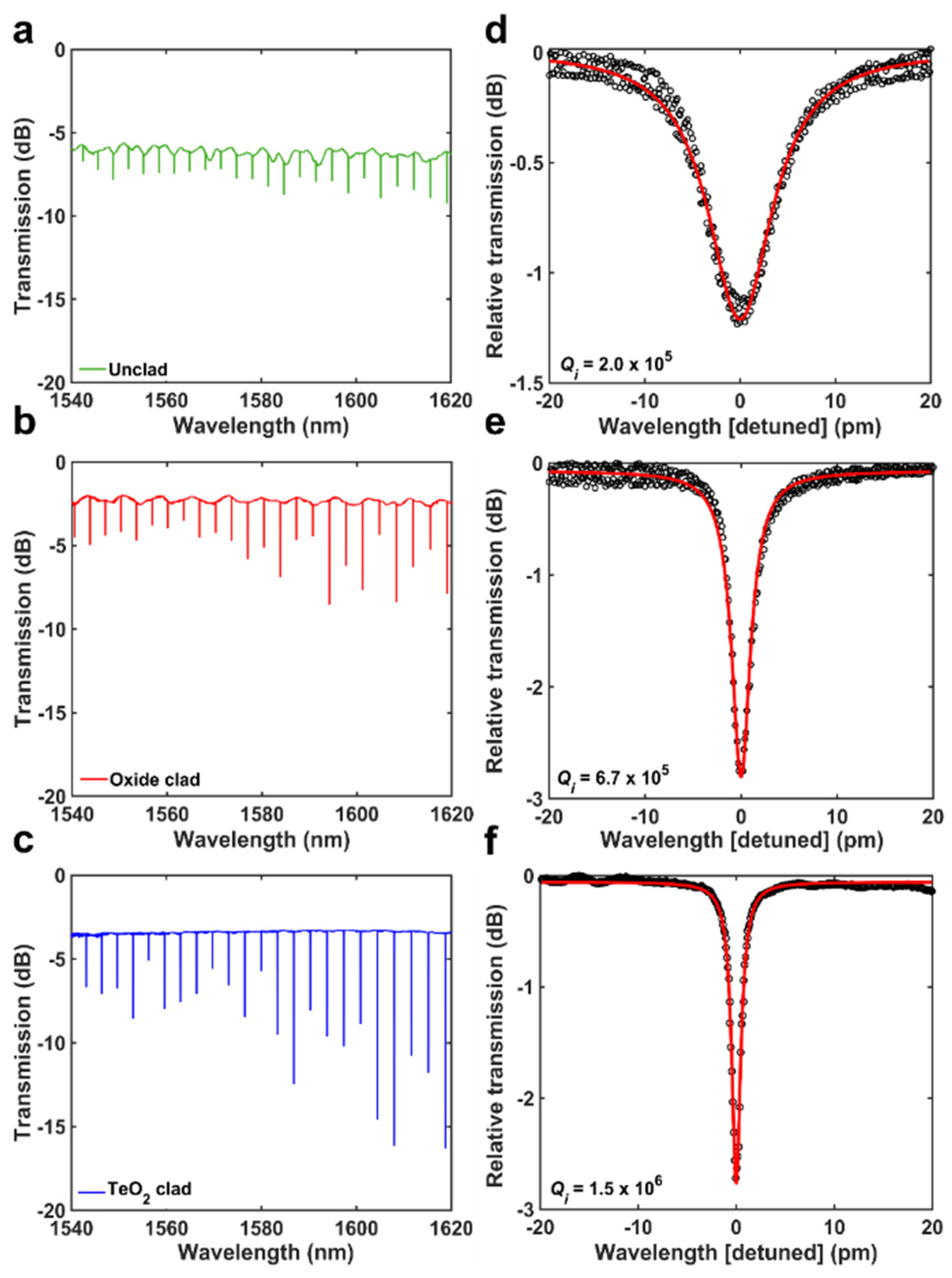
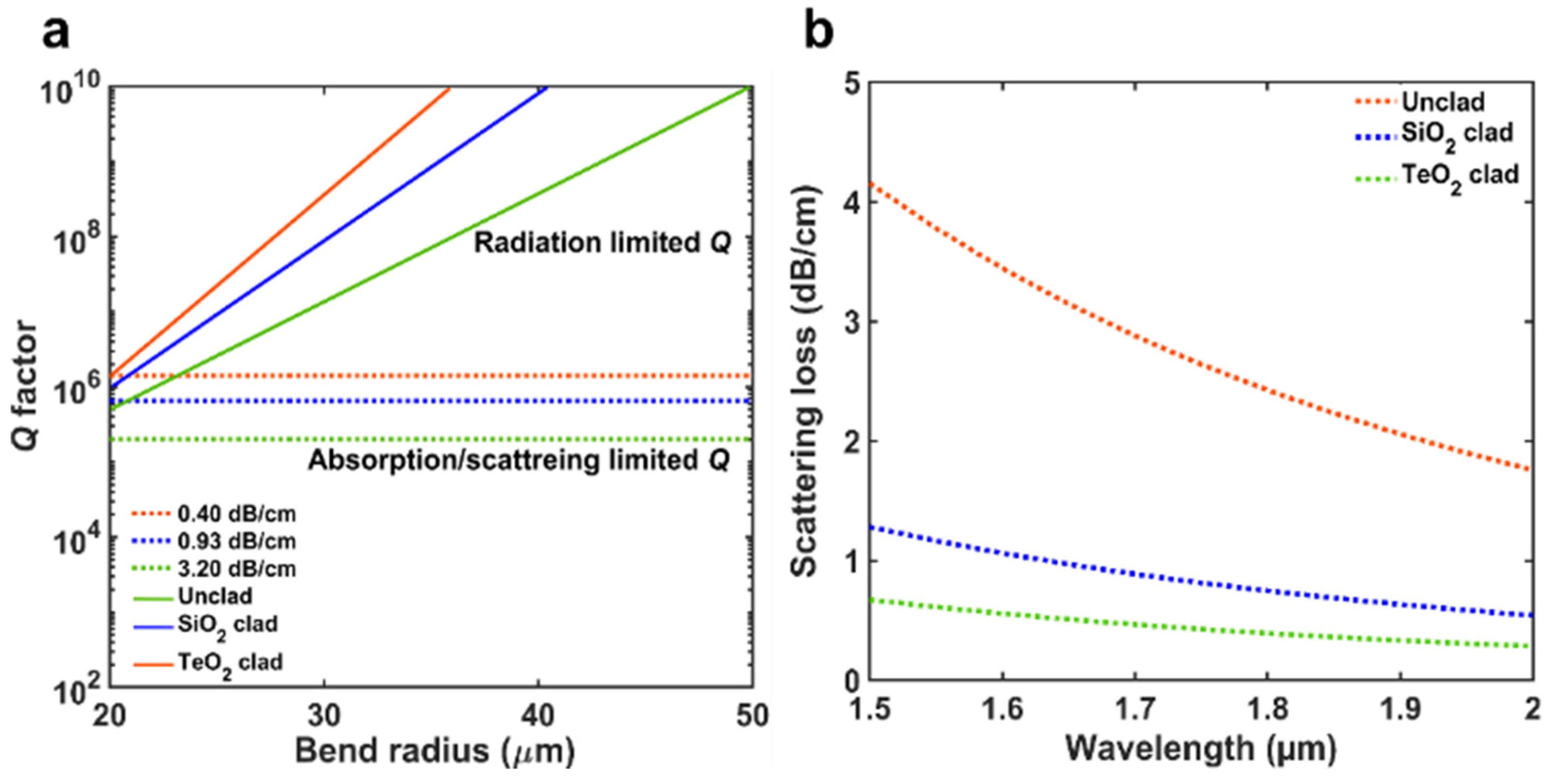
3. Microring Resonator Characterization

We used a fiber–chip edge coupling setup, a tunable Agilent 81640A 1510–1640 nm laser, and a fiber probe station to characterize the passive transmission properties of the silicon microring resonators. TE-polarized light from a 1550 nm tunable laser was launched into the chip through the polarization controller and lensed fiber, and the transmitted light across the chip was launched to the output lensed fiber connected to the Agilent power sensor. We observed TE single-mode resonances supported by the microring resonator, as shown in Figure 3a–c. For the TeO2-coated silicon microring resonator, we measured a free spectral range (FSR) of 3.7 nm at a wavelength of 1573 nm. The air- and SiO2-clad devices were under-coupled over the measured transmission range, while the TeO2-clad MRR was under-coupled at shorter wavelengths and became critically coupled above ~1600 nm. By fitting the transmission responses of the under-coupled resonator using a Lorentzian function (as indicated in Figure 3d–f), we obtained internal quality factors, Qi, of 2.0 × 10⁵ at 1542.43 nm, 6.7 × 10⁵ at 1587.28 nm, and 1.5 × 10⁶ at 1579.94 nm for the uncoated, SiO2-coated, and TeO2-coated silicon MRRs, respectively, corresponding to 3.4 dB/cm, 0.97 dB/cm, and 0.42 dB/cm propagation losses in the microring [33]. The results are summarized in Table 1, including the TeO2 film loss measured by prism coupling on a witness sample, showing low material loss, and fitted external and internal Q factors for the MRRs with different top claddings.
The total loss in the MRR can be expressed as the losses from the bulk materials, including contributions from the Si, SiO2, and TeO2 linear absorption and Si nonlinear (two-photon) absorption, radiation loss due to waveguide bends, and surface scattering losses related to the waveguide surface roughness and geometry. The bulk loss includes losses from impurities, internal defects, absorption loss due to chemical bonds, and nano- and micro-voids. Because of the high-quality silicon-on-insulator and SiO2 foundry materials, and low TeO2 film loss, we expected the bulk material loss contribution to be negligible. Furthermore, nonlinear optical loss was anticipated to be low due to the low power used in the transmission experiments.
We calculated the theoretical radiation loss and equivalent Q factor for the TeO2-coated silicon microring resonator structure using an FEM bent eigenmode solver, for varying bend radii, as shown in Figure 4a. The dashed lines in Figure 4a indicate the experimentally determined internal Q factors for the MRRs with different claddings. The calculated radiation-limited Q factors were measured to be 3 × 10⁸, 1 × 10⁸, and 1.7 × 10⁷ for the TeO2-clad, SiO2-clad, and unclad microring resonators, respectively, at a radius of 30 µm, corresponding to 0.002 dB/cm, 0.007 dB/cm, and 0.04 dB/cm propagation losses. The results show that the radiation loss was low (Q > 107) at the selected bend radius of 30 µm.
The surface scattering loss is the waveguide scattering loss per unit length and was calculated using the widely used Payne–Lacey model [34]. This model has been applied previously to 3D-SOI bent waveguides [35,36,37] such that
α S u r f a c e   S c a t t e r i n g = 4.34 σ 2 2 k 0 ( W 2 ) 4 n 1 f . g . η
where σ, k0, W, and n1 are the roughness, free-space wave vector, waveguide width, and core index, respectively. The function f is determined by the correlation length (Lc), while g is determined by the geometry of the waveguide and accounts for ridge-type waveguide structures such as the SOI ridge rings investigated here. Both σ and Lc are typically measured via atomic force microscopy or scanning electron microscopy of a waveguide. We assumed values of 1.0 nm and 50 nm for σ and Lc, respectively, based on previous measurements on SOI waveguides [35,36,37,38]. We also assumed the roughness of the TeO2 coating can be neglected based on previous AFM roughness measurements showing <1 nm root mean square (RMS) surface roughness on low-loss sputtered thin films [38]. Details of the expressions g and f can be found in the Payne–Lacey model [34]. The Payne–Lacey model was modified for bent waveguides and rings by adding a correction factor η [35] which allows us to accurately predict the loss of bent waveguides or resonators given the value of the sidewall roughness. The correction factor η is defined as the ratio of the mode overlap between bent and straight waveguides using an FEM simulation. In the Payne–Lacey bending model, η is considered 1 in the straight waveguide. We plot the sidewall scattering loss as a function of the wavelength in Figure 4b. The experimental loss obtained from the quality factor measurements of the MRRs follows the same trend as the Payne–Lacey model, which indicates that the losses in the different MRRs are largely influenced by the core cladding refractive index contrast and sidewall roughness [23]. These results show that the application of a high-refractive-index TeO2 top cladding can be considered promising for low-loss passive components as well as active devices such as monolithic amplifiers and lasers with improved performance on the SOI platform [32].

4. Conclusions

In summary, we have demonstrated a compact, single-mode TeO2–Si hybrid microring resonator with a 1.5 × 10⁶ internal Q factor corresponding to a 0.42 dB/cm propagation loss. The resonator was fabricated using a standard wafer-scale foundry process and a simple post-processing TeO2 deposition step at room temperature. We propose that these results on tellurium oxide-coated silicon microring resonators are promising for the fabrication of integrated on-chip low-cost and high-performance rare-earth-doped active devices such as amplifiers and lasers, as well as low-loss passive and nonlinear devices in silicon photonic platforms, with signal processing, light generation, microwave photonics, environmental and biological sensing, and communications applications.

Author Contributions

K.M.K. designed the device; K.M.K. and D.B.B. laid out the silicon chips. K.M.K. developed the low-loss tellurium oxide films on the silicon chips. K.M.K. performed the experimental characterization and analysis. K.M.K. wrote the original manuscript. A.P.K. and J.D.B.B. reviewed and edited the text. A.P.K. and J.D.B.B. supervised the project. All authors have read and agreed to the published version of the manuscript.

Funding

This research was funded by the Natural Sciences and Engineering Research Council of Canada (grant numbers RGPIN-2017-06423, STPGP 494306, and RTI-2017-00474), the Canadian Foundation for Innovation (CFI project number 35548), and the Ontario Research Fund (ORF project numbers 35548 and RE-09-051).

Institutional Review Board Statement

Not applicable.

Informed Consent Statement

Not applicable.

Data Availability Statement

The data presented in this study are available on request from the corresponding author.

Acknowledgments

We thank CMC Microsystems and the SiEPIC Program for facilitating the silicon photonics fabrication, and the Centre for Emerging Device Technologies (CEDT) at McMaster University for support with the reactive sputtering system.

Conflicts of Interest

The authors declare no conflict of interest.

References

  1. Thomson, D.; Zilkie, A.; Bowers, J.E.; Komljenovic, T.; Reed, G.T.; Vivien, L.; Marris-Morini, D.; Cassan, E.; Virot, L.; Fédéli, J.-M.; et al. Roadmap on silicon photonics. J. Opt. 2016, 18, 073003. [Google Scholar] [CrossRef]
  2. Baets, R.; Subramanian, A.Z.; Clemmen, S.; Kuyken, B.; Bienstman, P.; Le Thomas, N.; Roelkens, G.N.; Van Thourhout, D.; Helin, P.; Severi, S. Silicon Photonics: Silicon nitride versus silicon-on-insulator. In Proceedings of the Optical Fiber Communications Conference and Exhibition, Anaheim, CA, USA, 20–22 March 2016. [Google Scholar]
  3. Watts, M.R.; Shaw, M.J.; Nielson, G.N. Optical Resonators: Microphotonic Thermal Imaging. Nat. Photonics 2007, 1, 632. [Google Scholar] [CrossRef]
  4. Tran, M.A.; Huang, D.; Komljenovic, T.; Peters, J.; Malik, A.; Bowers, J.E. Ultra-Low-Loss Silicon Waveguides for Heterogeneously Integrated Silicon/III-V Photonics. Appl. Sci. 2018, 8, 1139. [Google Scholar] [CrossRef] [Green Version]
  5. Xiang, C.; Jin, W.; Guo, J.; Williams, C.; Netherton, A.M.; Chang, L.; Morton, P.A.; Bowers, J.E. Effects of nonlinear loss in high-Q Si ring resonators for narrow-linewidth III-V/Si heterogeneously integrated tunable lasers. Opt. Express 2020, 28, 19926–19936. [Google Scholar] [CrossRef] [PubMed]
  6. Biberman, A.; Bergman, K. Optical interconnection networks for high performance computing system. Rep. Prog. Phys. 2012, 75, 046402. [Google Scholar] [CrossRef]
  7. Xiao, S.; Khan, M.H.; Shen, H.; Qi, M. Multiple-channel silicon micro-resonator-based filters for WDM applications. Opt. Express 2007, 15, 7489–7498. [Google Scholar] [CrossRef] [PubMed]
  8. Salih Magden, E.; Li, N.; Purnawirman; Bradley, J.D.B.; Singh, N.; Ruocco, A.; Petrich, G.S.; Leake, G.; Coolbaugh, D.D.; Ippen, E.P.; et al. Monolithically-integrated distributed feedback laser compatible with CMOS processing. Opt. Express 2017, 25, 18058–18065. [Google Scholar] [CrossRef] [PubMed]
  9. Stern, B.; Ji, X.; Dutt, A.; Lipson, M. Compact narrow-linewidth integrated laser based on a low-loss silicon nitride ring resonator. Opt. Lett. 2017, 42, 4541–4544. [Google Scholar] [CrossRef] [PubMed]
  10. Sun, Y.; Fan, X. Optical ring resonators for biochemical and chemical sensing. Analytical and Bioanalytical Chemistry. Anal. Bioanal. Chem. 2011, 399, 205–211. [Google Scholar] [CrossRef] [PubMed]
  11. Ji, M.; Cai, H.; Deng, L.; Huang, Y.; Huang, Q.; Xia, J.; Li, Z.; Yu, J.; Wang, Y. Enhanced parametric frequency conversion in a compact silicon-graphene microring resonator. Opt. Express 2015, 23, 18679–18685. [Google Scholar] [CrossRef] [PubMed]
  12. Miarabbas Kiani, K.; Mbonde, H.M.; Frankis, H.C.; Mateman, R.; Leinse, A.; Knights, A.P.; Bradley, J.D.B. Four-wave mixing in high-Q tellurium-oxide-coated silicon nitride microring resonators. OSA Contin. 2020, 3, 3497–3507. [Google Scholar] [CrossRef]
  13. Grassani, D.; Azzini, S.; Liscidini, M.; Galli, M.; Strain, M.J.; Sorel, M.; Sipe, J.E.; Bajoni, D. Micrometer-scale integrated silicon source of time-energy entangled photons. Optica 2015, 2, 88–94. [Google Scholar] [CrossRef] [Green Version]
  14. La Notte, M.; Troia, B.; Muciaccia, T.; Campanella, C.E.; De Leonardis, F.; Passaro, V.M. Recent advances in gas and chemical detection by Vernier effect-based photonic sensors. Sensors 2014, 14, 4831–4855. [Google Scholar] [CrossRef] [PubMed]
  15. Rabus, D.G.; Hamacher, M.; Troppenz, U.; Heidrich, H. Optical filters based on ring resonators with integrated semiconductor optical amplifiers in GaInAsP-InP. IEEE. J. Sel. Top. Quant. 2002, 8, 1405–1411. [Google Scholar] [CrossRef]
  16. Dubray, O.; Seyedi, M.A.; Chen, C.H.; Charbonnier, B.; Descos, A.; Fiorentino, M.; Beausoleil, R.G.; Menezo, S. 30 Gbit/s PAM-4 transmission by modulating a dual silicon ring resonator modulator. In Proceedings of the Optical Interconnects Conference, San Diego, CA, USA, 9–11 May 2016. [Google Scholar]
  17. Luo, L.; Wiederhecker, G.S.; Cardenas, J.; Poitras, C.; Lipson, M. High quality factor etchless silicon photonic ring resonators. Opt. Express 2011, 19, 6284–6289. [Google Scholar] [CrossRef] [PubMed]
  18. Griffith, A.; Cardenas, J.; Poitras, C.B.; Lipson, M. High quality factor and high confinement silicon resonators using etchless process. Opt. Express 2012, 20, 21341–21345. [Google Scholar] [CrossRef] [PubMed]
  19. Dong, P.; Qian, W.; Liao, S.; Liang, H.; Kung, C.; Feng, N.; Shafiiha, R.; Fong, J.; Feng, D.; Krishnamoorthy, A.V.; et al. Low loss shallow-ridge silicon waveguides. Opt. Express 2010, 18, 14474–14479. [Google Scholar] [CrossRef] [PubMed]
  20. Guill, M.A.; Caverley, M.; Cretu, E.; Jaeger, N.A.F.; Chrostowski, L. Large-Area, High- Q SOI Ring Resonators. IEEE Photon. Conf. IPC 2014, 4, 336–337. [Google Scholar]
  21. Burla, M.; Crockett, B.; Chrostowski, L.; Azaña, J. Ultra-high Q multimode waveguide ring resonators for microwave photonics signal processing. In Proceedings of the International Topical Meeting on Microwave Photonics, Paphos, Cyprus, 26–29 October 2015. [Google Scholar]
  22. Zhang, Y.; Hu, X.; Chen, D.; Wang, L.; Li, M.; Feng, P.; Xiao, X.; Yu, S. Design and demonstration of ultra-high-Q silicon microring resonator based on a multi-mode ridge waveguide. Opt. Lett. 2018, 43, 1586–1589. [Google Scholar]
  23. Zhang, L.; Jie, L.; Zhang, M.; Wang, Y.; Xie, Y.; Shi, Y.; Dai, D. Ultrahigh-Q silicon racetrack resonators. Photon. Res. 2020, 8, 684–689. [Google Scholar] [CrossRef]
  24. Biberman, A.; Shaw, M.J.; Timurdogan, E.; Wright, J.B.; Watts, M.R. Ultralow-loss silicon ring resonators. Opt. Lett. 2012, 37, 4236–4238. [Google Scholar] [CrossRef] [PubMed]
  25. Nezhad, M.P.; Bondarenko, O.; Khajavikhan, M.; Simic, A.; Fainman, Y. Etch-free low loss silicon waveguides using hydrogen silsesquioxane oxidation masks. Opt. Express 2011, 19, 18827–18832. [Google Scholar] [CrossRef] [PubMed]
  26. Bellegarde, C.; Pargon, E.; Sciancalepore, C.; Petit-Etienne, C.; Hugues, V.; Robin-Brosse, D.; Hartmann, J.; Lyan, P. Improvement of Sidewall Roughness of Submicron SOI Waveguides by Hydrogen Plasma and Annealing. IEEE Photon. Technol. Lett. 2018, 30, 591–594. [Google Scholar] [CrossRef]
  27. Horikawa, T.; Shimura, D.; Mogami, T. Low-loss silicon wire waveguides for optical integrated circuits. MRS Commun. 2016, 6, 9–15. [Google Scholar] [CrossRef]
  28. Frankis, H.C.; Miarabbas Kiani, K.; Bonneville, D.B.; Zhang, C.; Norris, S.; Mateman, R.; Leinse, A.; Bassim, N.D.; Knights, A.P.; Bradley, J.D.B. Low-loss TeO2-coated Si3N4 waveguides for application in photonic integrated circuits. Opt. Express 2019, 27, 12529–12540. [Google Scholar] [CrossRef]
  29. Miarabbas Kiani, K.; Frankis, H.C.; Mbonde, H.M.; Mateman, R.; Leinse, A.; Knights, A.P.; Bradley, J.D.B. Thulium-doped tellurium oxide waveguide amplifier with 7.6 dB net gain on a silicon nitride chip. Opt. Lett. 2019, 44, 5788–5791. [Google Scholar] [CrossRef]
  30. Miarabbas Kiani, K.; Frankis, H.C.; Mateman, R.; Leinse, A.; Knights, A.P.; Bradley, J.D.B. Thulium-doped tellurium oxide microring lasers integrated on a low-loss silicon nitride platform. Opt. Mater. Express 2021, 11, 3656–3665. [Google Scholar] [CrossRef]
  31. Jha, A.; Richards, B.; Jose, G.; Teddy-Fernandez, T.; Joshi, P.; Jiang, X.; Lousteau, J. Rare-earth ion doped TeO2 and GeO2 glasses as laser materials. Prog. Mater. Sci. 2012, 57, 1426–1491. [Google Scholar] [CrossRef]
  32. Miarabbas Kiani, K.; Frankis, H.C.; Naraine, C.M.; Bonneville, D.B.; Knights, A.P.; Bradley, J.D.B. Lasing in a hybrid rare-earth silicon microdisk. Laser Photon. Rev. 2022, 16, 210034. [Google Scholar] [CrossRef]
  33. Preston, K.; Schmidt, B.; Lipson, M. Polysilicon photonic resonators for large-scale 3D integration of optical networks. Opt. Express 2013, 15, 17283–17290. [Google Scholar] [CrossRef]
  34. Payne, F.P.; Lacey, J.P.R. A theoretical analysis of scattering loss from planar optical waveguides. Opt. Quantum Electron. 1994, 26, 977–986. [Google Scholar] [CrossRef]
  35. Hagan, D.E.; Knights, A.P. Mechanisms for optical loss in SOI waveguides for mid-infrared wavelengths around 2 μm. J. Opt. 2017, 19, 025801. [Google Scholar] [CrossRef]
  36. Yap, K.P.; Delâge, A.; Lapointe, J.; Lamontagne, B.; Schmid, J.H.; Waldron, P.; Syrett, B.A.; Janz, S. Correlation of Scattering Loss, Sidewall Roughness and Waveguide Width in SiO2/Si Silicon-on-Insulator (SOI) Ridge Waveguides. J. Lightwave Technol. 2009, 27, 3999–4008. [Google Scholar]
  37. Shang, H.; Sun, D.; Yu, P.; Wang, B.; Yu, T.; Li, T.; Jiang, H. Investigation for Sidewall Roughness Caused Optical Scattering Loss of Silicon-on-Insulator Waveguides with Confocal Laser Scanning Microscopy. Coatings 2020, 10, 236. [Google Scholar] [CrossRef] [Green Version]
  38. Miller, J.W.; Chesaux, M.; Deligiannis, D.; Mascher, P.; Bradley, J.D.B. Low-loss GeO2 thin films deposited by ion-assisted alternating current reactive sputtering for waveguide applications. Thin Solid Films 2020, 709, 13816. [Google Scholar] [CrossRef]
Figure 1. (a) Cross-section profile of the TeO2-coated Si microring showing the microring structure. (b) Top-view SEM image of a TeO2-coated Si microring resonator. (c) Photograph of the coupling setup during measurement showing the SOI chip with window opening for TeO2 post-processing deposition. (d) Microscopic image of the open window microring resonator structure.
Applsci 12 01363 g001
Figure 2. Calculated electric field profile of the fundamental transverse-electric (TE)-polarized mode for (a) unclad, (b) SiO2-clad, and (c) TeO2-clad silicon microring resonators. (d) Calculated fractional optical intensity overlap factors and effective mode areas for the fundamental TE microring mode at 1550 nm wavelength.
Applsci 12 01363 g002
Figure 3. Measured TE transmission spectra for (a) uncoated, (b) SiO2-coated, and (c) TeO2-coated silicon microring resonators with a microring–waveguide gap of 1.0 μm. Close-up views of the under-coupled resonances for the (d) uncoated, (e) SiO2-coated, and (f) TeO2-coated silicon microring resonators showing an intrinsic quality factor, Qi, of 1.5 × 10⁶, corresponding to 0.42 dB/cm optical propagation loss for the TeO2-coated silicon microring resonator.
Applsci 12 01363 g003
Figure 4. (a) Calculated internal Q factor of uncoated-, SiO2-coated, and TeO2-coated silicon resonator waveguides versus bend radius. (b) Calculated scattering loss as a function of wavelength for microring resonators with air, SiO2, and TeO2 claddings based on the 3D Payne–Lacey model.
Applsci 12 01363 g004
Table 1. Measured properties of silicon microring resonators with different cladding materials.
Cladding MaterialCladding Thickness (nm)Film Loss @ 638 nm (dB/cm)Film Loss @ 1550 nm (dB/cm)Extinction Ratio (dB)External Q FactorInternal Q FactorPropagation Loss (dB/cm)
Uncladded------------1.22.8 × 1062.0 × 1053.4
SiO22000--------2.84.2 × 1066.7 × 1050.97
TeO22700.5 ± 0.20.1 ± 0.12.89.0 × 1061.5 × 1060.42
Publisher’s Note: MDPI stays neutral with regard to jurisdictional claims in published maps and institutional affiliations.

