Communication

A Wideband Microstrip-to-Waveguide Transition Using E-Plane Probe with Parasitic Patch for W-Band Application

1
Institute of Systems Engineering, Academy of Military Sciences, Beijing 100082, China
2
National Innovation Institute of Defense Technology, Academy of Military Sciences, Beijing 100082, China
*
Authors to whom correspondence should be addressed.
Appl. Sci. 2022, 12(23), 12162; https://doi.org/10.3390/app122312162
Submission received: 3 November 2022 / Revised: 22 November 2022 / Accepted: 25 November 2022 / Published: 28 November 2022

Abstract

:
The hollow metal waveguides are attractive components for millimeter-wave circuits owing to low loss. To integrate with the front-end circuit, a transition from microstrip line to waveguide is required. In this article, a microstrip-to-waveguide transition is presented in the W-band by using an E-plane probe with a parasitic patch. The probe is embedded into the waveguide along the center of the broad wall to excite the TE10 mode. A backshort-circuited waveguide with a quarter wavelength is used to obtain sufficient energy coupling and achieve good impedance matching. The additional parasitic patch can introduce a new resonance at a low frequency to enhance the working bandwidth. Hence, the proposed transition achieves wide working bandwidth and low insertion loss. For verification, a back-to-back transition is constructed and measured. The measured results indicate that the proposed transition has a wide working bandwidth covering the entire W-band. The measured reflection coefficient is below −13 dB from 70 to 110 GHz and the average insert loss is 1.1 dB. Attributed to wide working bandwidth and simple structure, the proposed transition is attractive for W-band circuit systems.

1. Introduction

Owing to the development of integrated circuits (ICs), the millimeter wave spectrum has been receiving more and more attention. Many applications in the millimeter-wave band are under development, such as 5G communication [1], 77/79 GHz automotive radars [2,3], wireless backhaul [4], and 94 GHz radar/imaging systems [5,6]. Benefiting from the low loss and high power capacity, the waveguide components are widely used in millimeter-wave systems, such as high-Q filters, horn antennas, power dividers, etc. However, waveguide components cannot be directly connected to the monolithic microwave integrated circuits (MMIC). The microstrip line is an essential component for interconnecting with the MMIC. Thus, a microstrip-to-waveguide transition is required to integrate the waveguide with the MMIC.
Various technologies have been explored for realizing microstrip to waveguide transition. In [7,8,9,10], these transitions using a multi-stage impedance transformer can achieve wide working bandwidth. For example, a microstrip-to-waveguide transition is presented in [8] by coupling energy from the microstrip line to the stepped ridge and subsequently to the rectangular waveguide. The transition achieves working bandwidth of 38% from 50 to 72 GHz and insertion loss below 0.4 dB. However, the disadvantage of this type of structure is that they have a large volume due to the multi-section waveguide or ridge for the impedance transformer. The transitions employing antipodal fin-line [11,12,13,14] are another type of broadband structure. However, they require a relatively long length to realize wide bandwidth. A microstrip-to-waveguide transition based on an H-plane split waveguide is proposed in [15]. The conversion from microstrip mode to TE10 mode of the waveguide is realized by a resonant cavity. The transition realizes a working bandwidth of 35%. In [16], the transition using quasi-Yagi antenna is designed and it achieves a bandwidth of 35%. However, the quasi-Yagi antenna requires a high dielectric constant substrate to achieve a shorter arm length for mounting to the waveguide. The E-plane probe-type transition has the characteristic of low insertion loss and wide impedance bandwidth. Several in-line transitions based on an E-plane probe or dipole are proposed in [17,18,19,20]. They achieve wide working bandwidth covering full-band and low insertion loss. Nevertheless, an extra bend waveguide will be required if the input and output ports need to be arranged vertically, which will cause additional loss and large volume. An E-plane probe vertical transition from the microstrip line to the waveguide is reported in [21]. The probe deviates from the center of the waveguide to obtain a good impedance matching, which will increase the difficulty of manufacturing and assembly.
In this work, an E-plane probe transition with a perpendicular arrangement is proposed in W-band. The probe is embedded along the center of the waveguide broad wall to excite the TE10 mode. To improve impedance matching, a parasitic patch is introduced to the E-plane probe. The introduction of the parasitic patch generates a new resonance mode. Therefore, both bandwidth and impedance matching can be improved. The proposed transition can achieve wide impedance bandwidth covering the full W-band with a reflection coefficient below −20 dB. Moreover, a back-to-back is designed and fabricated for verification. The experimental results prove a good performance of the transition.

2. Transition Structure and Design

2.1. Working Principle and the Design of Transition

E-plane probes are a class of typical structures for achieving mode conversion from the quasi-TEM mode of the microstrip line and the TE10 mode of the rectangular waveguide. Figure 1 shows electric field diagrams of modes to clarify the working principle. When the E-plane probe is embedded in the rectangular waveguide, it can be considered as a coaxial line surrounded by the adjacent waveguide walls. The cross-sectional electric field (E-field) of the probe is shown in Figure 1a. The E-field is generated between the probe and the waveguide wall above the probe. Figure 1b displays the cross-sectional E-field of rectangular waveguide TE10 mode. The wave vector (k) is along the z-direction. Therefore, to convert microstrip mode to waveguide mode, the extension direction of the E-plane probe should be parallel to the vector E-field of TE10 mode. This relationship can be described as
P e E w
where Pe and Ew are the extension direction of the E-plane probe and the vector E-field of TE10 mode, respectively. Figure 2 presents the E-field distribution of a backshort-circuited waveguide. It can be found that the E-field at the center reaches maximum at a quarter wavelength from the short-circuited surface. Thus, the above transition structure requires a backshort-circuited waveguide with a quarter wavelength for sufficient energy coupling and good impedance matching.
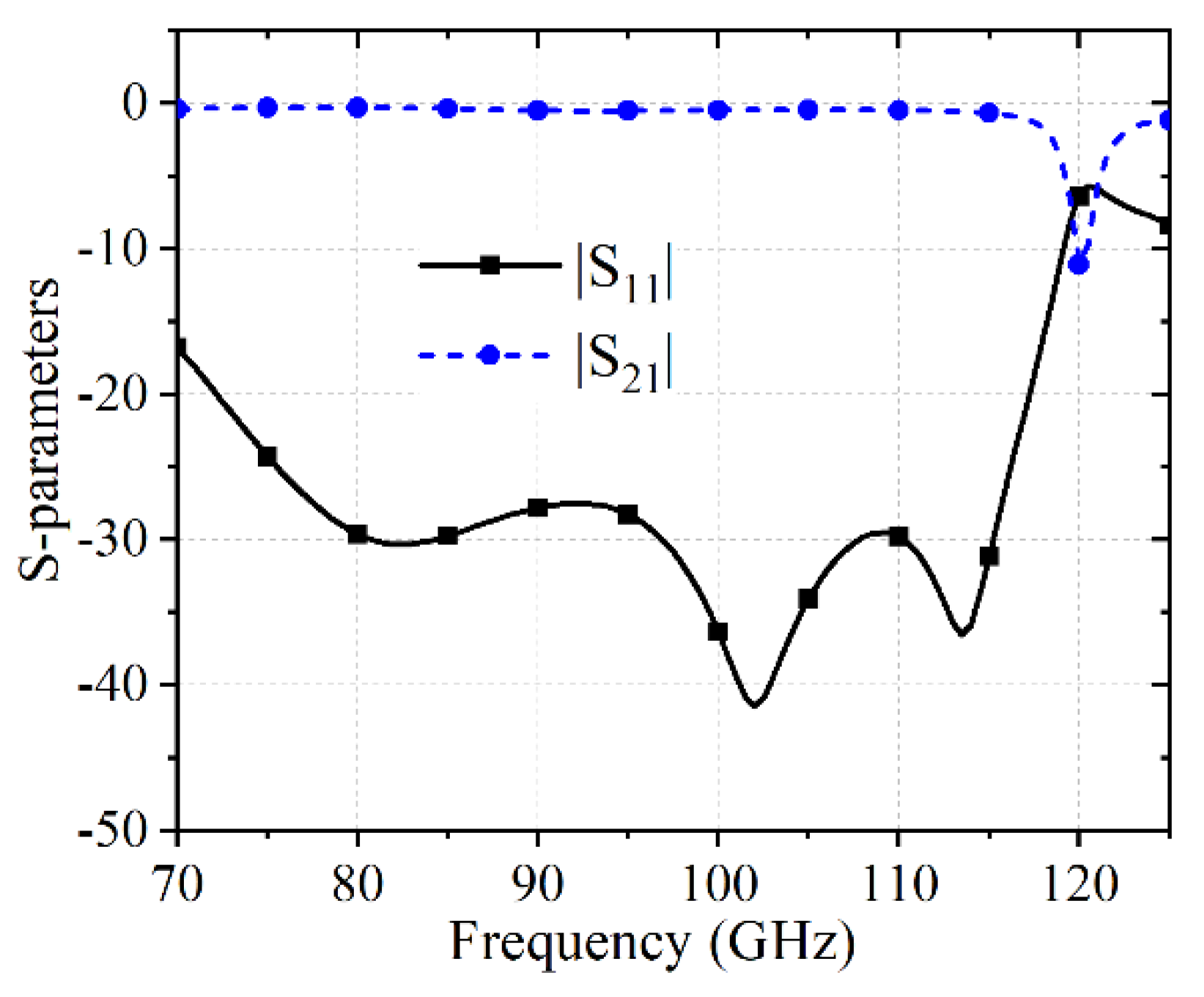
Based on the above operating mechanism, a microstrip-to-waveguide transition is designed in the W-band. Figure 3 shows the configuration of the proposed microstrip-to-waveguide transition. It consists of an input 50 Ω microstrip line, an E-plane probe with parasitic patch, a backshort-circuited waveguide, and an output WR 10 waveguide. The probe is connected to the end of the microstrip line and they are printed on a Ro 5880 substrate (permittivity ε r = 2.2, loss tangent δ = 0.0009) with the thickness of 0.127 mm. To suppress parallel plate modes and prevent the leakage of energy, the waveguide in the substrate metal is surrounded by metal vias. The E-plane probe is embedded along the center of the waveguide broadside to excite the TE10 fundamental mode. The backshort waveguide at the upper is usually λg/4 (λg is the operating wavelength at the center frequency). A groove is cut in the backshort waveguide to avoid contact between the microstrip line and the backshort waveguide. The transition is designed and optimized with the assistance of Ansys HFSS. Figure 4 shows the simulated S-parameters of the proposed transition. It can be seen that the reflection coefficient is less than −20 dB in the entire W-band. The transmission coefficient varies between −0.3 and −0.5 dB from 70 to 112 GHz. The optimized design parameters are given in Table 1.
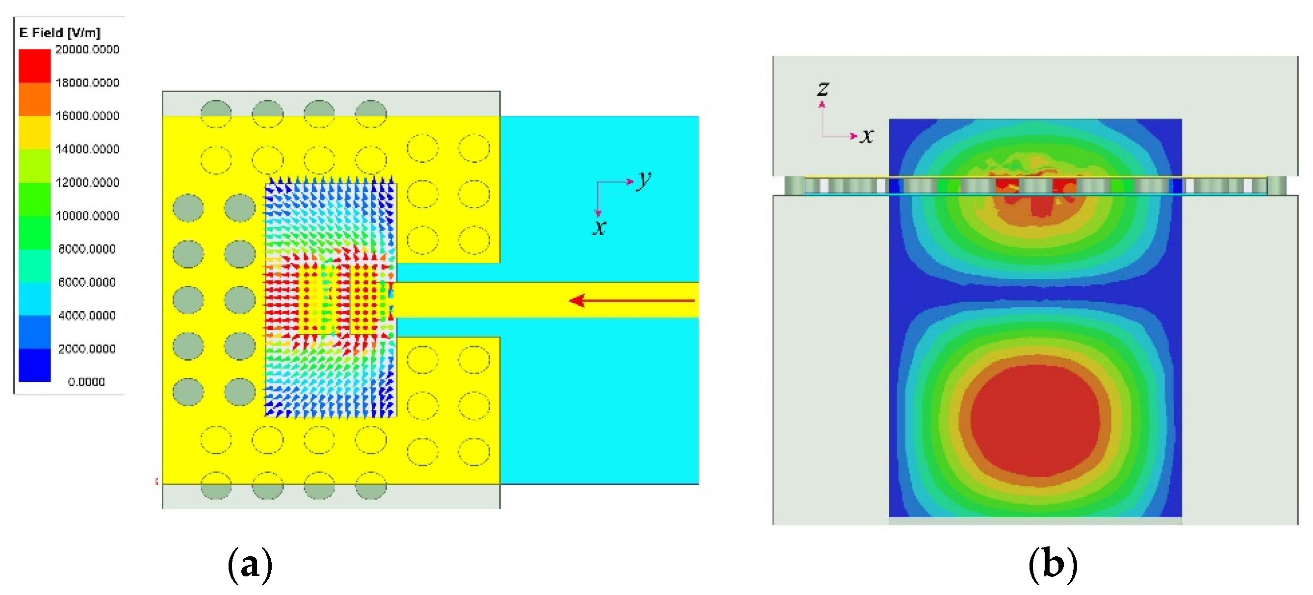
To verify the working principle, when the transition works at center frequency 90 GHz, the vector E-field on the probe and the cross-sectional E-field distribution in the rectangular waveguide are plotted in Figure 5. As shown in Figure 5a, the probe can couple energy to the parasitic patch through the gap. Thus, there is an intense E-field between the parasitic patch and probe. Then, a strong electric field is generated between the parasitic patch and the waveguide wall. The total E-field is along the –y-direction and it is similar to the E-field distribution of TE10 mode. As a result, it can be seen from Figure 5b that the TE10 mode is excited. The E-field distribution in Figure 5 verifies the correctness of the above working principle.

2.2. Parameter Analysis

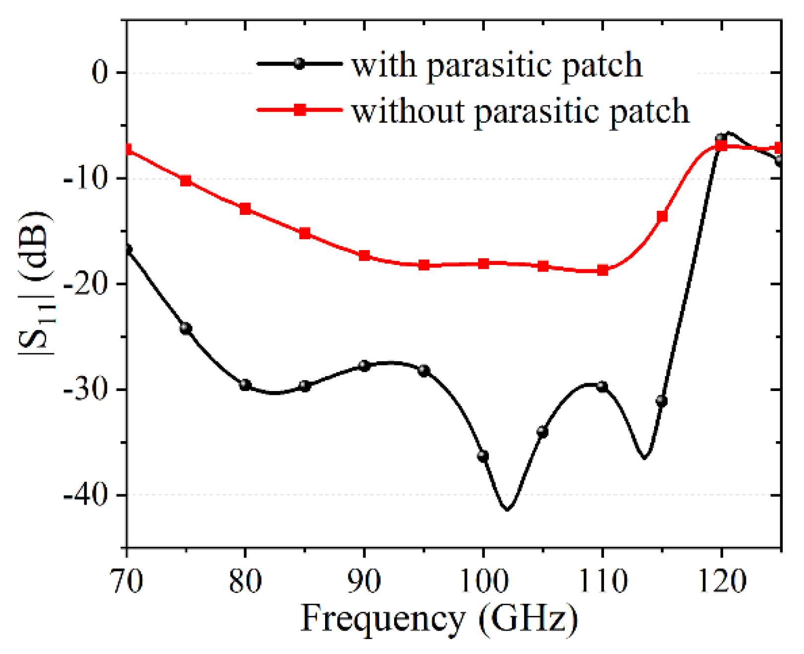
To better understand the design, several key parameters are studied. Figure 6 shows the effect of the probe with and without the parasitic patch on the reflection coefficient. It can be seen that the parasitic patch introduces a resonance at 80 GHz, which contributes to improving impedance matching and enhancing bandwidth. Compared with an alone probe, the probe with the parasitic patch can significantly improve the impedance matching in the whole W-band, especially in the lower frequency band. To further investigate the effect of the parasitic patch, the length of the parasitic patch is studied. Figure 7 shows the variation of the S-parameters with different lengths of the parasitic patch. The first resonant point is sensitive to the length l2. As the length l2 increases, the first resonant point moves to lower frequencies while the other resonant points are almost unchanged. However, a larger value of l2 will deteriorate the impedance matching at higher frequencies. Hence, a moderate value of l2 = 0.4 mm is selected to achieve a wideband impedance bandwidth covering the W-band. Figure 8 shows the influence of groove width on the performance of transition. It can be found that the second and third resonant points are affected by the width W2. As W2 increases, the second resonant point moves to higher frequencies while the third resonant point shifts toward lower frequencies. When the W2 is 0.9 mm, the second and third resonance points have the same resonant frequency. Meanwhile, the variation of groove width W2 has a significant effect on transmission zeros outside the passband. Although the transmission zero is far away from the desired frequency band, it moves to lower frequencies with the increase of W2. Hence, the groove width should be as small as possible when designing the transition.

3. Results and Discussion

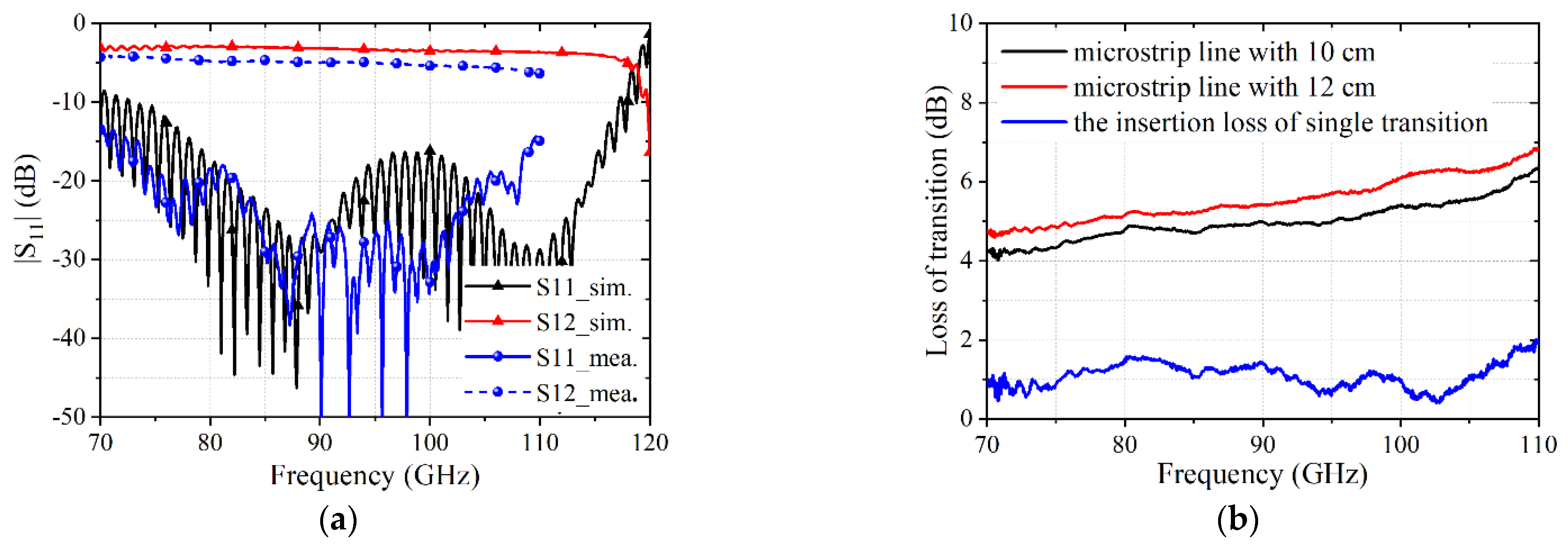
The simulated results of the proposed transition exhibit wide impedance bandwidth and low insertion loss. For experimental verification, a back-to-back microstrip-to-waveguide is designed and fabricated. Figure 9 shows the photograph of the fabricated prototype. All components of the transition are processed in blocks and then assembled with screws. The metal parts are made of aluminum, and the substrate part uses single-layer Roger RT/Duroid 5880. Agilent network analyzer N5245A and a pair of frequency expansion components are used to measure the S-parameters of the back-to-back transition. The measured and simulated results are shown in Figure 10a, where the length of the microstrip line is 10 cm. The measured results show that a reflection coefficient below −15 dB can be obtained in the entire W-band. Meanwhile, it can be observed that there is a good agreement between the simulated and measured reflection coefficients. The measured transmission coefficient is lower than the simulated one, especially in the higher frequency band. The deviation between transmission coefficients can be attributed to two aspects. On the one hand, the loss tangent of Ro 5880 provided by the manufacturer is measured at 10 GHz, which may not be accurate in W-band. The design experience indicates that the loss tangent rises with frequency. Thus, the loss tangent at W-band will be higher than the nominal one. On the other hand, the conductor loss cannot be ignored because the metal components are not gold-plated. To estimate the insertion loss of the proposed transition, the second back-to-back transition with the 12 cm length of the microstrip line is fabricated and measured. Figure 10b shows the measured insertion losses with different lengths of the microstrip line. After calculation, the average loss of the microstrip line is about 0.28 dB/cm in W-band. The calculated insertion loss of a single transition is shown in Figure 10b, with an average value of about 1.2 dB. The calculated insert loss for a single transition has a relatively high value due to the fact that the conductor loss is not eliminated.
A performance comparison of our work and some up-to-date transitions are summarized in Table 2. To achieve wide bandwidth, the transition in [8] with multi-stage ridge and transition in [11] with long antipodal slot line are designed, which results in a large size. The metal pins in [11] and additional branch waveguide in [17] increase the fabricated complexity. In [19], a microstrip-to-waveguide is designed on quartz substrate by using a quasi-Yagi antenna. However, the stub arrays and indented waveguide are required to suppress the rectangular cavity resonances, which makes whole structure more complex. The transition in [21] is similar to our work. However, the bandwidth and insertion loss of transition using common probe are not so satisfactory. This comparison verifies the advantages of the proposed transition in terms of bandwidth, compactness, and complexity. The insertion loss of the proposed transition is relatively high, but it may be improved by plating gold on the waveguide surface.

4. Conclusions

A wideband microstrip-to-waveguide transition is designed in W-band. The proposed transition is based on the E-plane probe to excite the TE10 mode of the waveguide. The working principle has been elaborated. In the design, a parasitic patch is introduced to the E-plane probe to obtain an additional resonance at a low frequency. The introduction of the parasitic patch can improve impedance matching and increase working bandwidth. The simulated results exhibit the excellent performance of the proposed transition. Moreover, for verification, a back-to-back transition was fabricated and measured. The measured results show that the proposed transition has a reflection coefficient below −13 dB from 70 to 110 GHz and an average insert loss of 1.1 dB. With good performance and a simple structure, the proposed transition is desirable for W-band application.

Author Contributions

Conceptualization, M.H. and C.W.; methodology, M.H.; software, C.W.; formal analysis, C.L.; investigation, S.X.; resources, J.M.; data curation, H.S.; writing—original draft preparation, M.H.; writing—review and editing, C.W.; visualization, M.H. and C.W.; supervision, H.S.; project administration, H.S.; funding acquisition, C.W. and C.L. All authors have read and agreed to the published version of the manuscript.

Funding

This research was funded by the National Natural Science Foundation of China under Grant 62104259 and Grant 62105370.

Data Availability Statement

Not applicable.

Conflicts of Interest

The authors declare no conflict of interest.

References

  1. Hong, W.; Jiang, Z.H.; Yu, C.; Zhou, J.; Chen, P.; Yu, Z.; Zhang, H.; Yang, B.; Pang, X.; Jiang, M.; et al. Multibeam Antenna Technologies for 5G Wireless Communications. IEEE Trans. Antennas Propag. 2017, 65, 6231–6249. [Google Scholar] [CrossRef]
  2. Ku, B.-H.; Schmalenberg, P.; Inac, O.; Gurbuz, O.D.; Lee, J.S.; Shiozaki, K.; Rebeiz, G.M. A 77–81-GHz 16-Element Phased-Array Receiver With ± 50° Beam Scanning for Advanced Automotive Radars. IEEE Trans. Antennas Propag. 2014, 62, 2823–2832. [Google Scholar] [CrossRef]
  3. Tan, Q.; Fan, K.; Yang, W.; Luo, G. Low Sidelobe Series-Fed Patch Planar Array with AMC Structure to Suppress Parasitic Radiation. Remote Sens. 2022, 14, 3597. [Google Scholar] [CrossRef]
  4. Fan, K.; Hao, Z.C.; Yuan, Q.; Luo, G.Q.; Hong, W. A Wideband High-Gain Planar Integrated Antenna Array for E-Band Backhaul Applications. IEEE Trans. Antennas Propag. 2020, 68, 2138–2147. [Google Scholar] [CrossRef]
  5. Chen, Z.; Zhang, Y.P.; Bisognin, A.; Titz, D.; Ferrero, F.; Luxey, C. An LTCC Microstrip Grid Array Antenna for 94-GHz Applications. IEEE Antennas Wirel. Propag. Lett. 2015, 14, 1279–1281. [Google Scholar] [CrossRef]
  6. Tamayo-Domínguez, A.; Fernández-González, J.M.; Sierra-Castañer, M. Monopulse Radial Line Slot Array Antenna Fed by a 3-D-Printed Cavity-Ended Modified Butler Matrix Based on Gap Waveguide at 94 GHz. IEEE Trans. Antennas Propag. 2021, 69, 4558–4568. [Google Scholar] [CrossRef]
  7. Zarba, G.; Bertin, G.; Besso, P. An optimised waveguide to microstrip transition at K band. In Proceedings of the 1996 26th European Microwave Conference, Prague, Czech Republic, 6–13 September 1996; pp. 836–838. [Google Scholar]
  8. Han, K.Y.; Pao, C.K. A V-band waveguide to microstrip inline transition. In Proceedings of the 2012 IEEE MTT-S International Microwave Symposium Digest, Montreal, QC, Canada, 17–22 June 2012; pp. 1–3. [Google Scholar]
  9. Pérez, J.M.; Rebollo, A.; Gonzalo, R.; Ederra, I. An inline microstrip-to-waveguide transition operating in the full W-Band based on a Chebyshev multisection transformer. In Proceedings of the 2016 10th European Conference on Antennas and Propagation (EuCAP), Davos, Switzerland, 10–15 April 2016; pp. 1–4. [Google Scholar]
  10. Zhang, Y.; Ruiz-Cruz, J.A.; Zaki, K.A.; Piloto, A.J. A Waveguide to Microstrip Inline Transition with Very Simple Modular Assembly. IEEE Micro. Wirel. Compon. Lett. 2010, 20, 480–482. [Google Scholar] [CrossRef]
  11. Zhang, Y.; Shi, S.; Martin, R.D.; Prather, D.W. Broadband SIW-to-Waveguide Transition in Multilayer LCP Substrates at W-Band. IEEE Micro. Wirel. Compon. Lett. 2017, 27, 224–226. [Google Scholar] [CrossRef]
  12. Bai, R.; Dong, Y.L.; Xu, J. Broadband Waveguide-to-Microstrip Antipodal Finline Transition without Additional Resonance Preventer. In Proceedings of the 2007 International Symposium on Microwave, Antenna, Propagation and EMC Technologies for Wireless Communications, Hangzhou, China, 16–17 August 2007; pp. 385–388. [Google Scholar]
  13. Mozharovskiy, A.; Artemenko, A.; Ssorin, V.; Maslennikov, R.; Sevastyanov, A. Wideband tapered antipodal fin-line waveguide-to-microstrip transition for E-band applications. In Proceedings of the 2013 European Microwave Conference, Nuremberg, Germany, 6–10 October 2013; pp. 1187–1190. [Google Scholar]
  14. Zhang, C.W. A novel W-band waveguide-to-microstrip antipodal finline transition. In Proceedings of the 2013 IEEE International Conference on Applied Superconductivity and Electromagnetic Devices, Beijing, China, 25–27 October 2013; pp. 166–168. [Google Scholar]
  15. Zaman, A.U.; Vassilev, V.; Zirath, H.; Rorsman, N. Novel Low-Loss Millimeter-Wave Transition from Waveguide-to-Microstrip Line Suitable for MMIC Integration and Packaging. IEEE Micro. Wirel. Compon. Lett. 2017, 27, 1098–1100. [Google Scholar] [CrossRef] [Green Version]
  16. Kaneda, N.; Qian, Y.; Itoh, T. A broad-band microstrip-to-waveguide transition using quasi-Yagi antenna. IEEE Trans. Microw. Theory Tech. 1999, 47, 2562–2567. [Google Scholar] [CrossRef]
  17. Xu, Z.; Xu, J.; Qian, C. Novel In-Line Microstrip-to-Waveguide Transition Based on E-Plane Probe T-Junction Structure. IEEE Micro. Wirel. Compon. Lett. 2021, 31, 1051–1054. [Google Scholar] [CrossRef]
  18. Wu, C.; Zhang, Y.; Li, Y.; Zhu, H.; Xiao, F.; Yan, B.; Xu, R. Millimeter-Wave Waveguide-to-Microstrip Inline Transition Using a Wedge-Waveguide Iris. IEEE Trans. Microw. Theory Tech. 2022, 70, 1087–1096. [Google Scholar] [CrossRef]
  19. Kim, J.; Choe, W.; Jeong, J. Submillimeter-Wave Waveguide-to-Microstrip Transitions for Wide Circuits Wafers. IEEE Trans. Terahertz Sci. Tech. 2017, 7, 440–445. [Google Scholar] [CrossRef]
  20. Tan, Q.; Fan, K.; Zhu, F.; Dai, X.; Qian, Y.; Luo, G.Q. A Wideband SICL-to-Waveguide Transition for Multilayer Planar Circuit Applications at V-Band. IEEE Micro. Wirel. Compon. Lett. 2022, 32, 1027–1030. [Google Scholar] [CrossRef]
  21. Sakakibara, K.; Hirono, M.; Kikuma, N.; Hirayama, H. Broadband and planar microstrip-to-waveguide transitions in millimter-wave band. In Proceedings of the 2008 International Conference on Microwave and Millimeter Wave Technology, Nanjing, China, 21–24 April 2008; pp. 1278–1281. [Google Scholar]
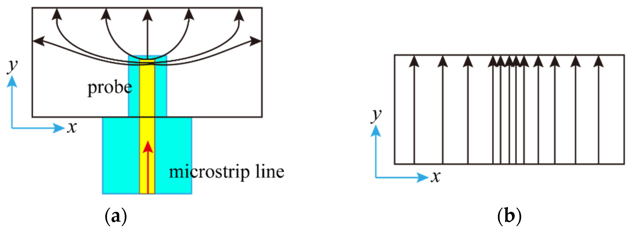
Figure 1. The electric field distribution of different structures. (a) The probe embedded in waveguide. (b) The TE10 mode of rectangular waveguide.
Applsci 12 12162 g001
Figure 2. The electric field distribution of short-circuited waveguide.
Applsci 12 12162 g002
Figure 3. The configuration of the proposed transition. (a) 3D view. (b) Top view.
Applsci 12 12162 g003
Figure 4. The simulated S-parameters of the proposed transition.
Applsci 12 12162 g004
Figure 5. The electric field distribution of the transition. (a) The vector E-field of the probe. (b) The cross-sectional E-field distribution in rectangular waveguide.
Applsci 12 12162 g005
Figure 6. Simulated reflection coefficient of the proposed transition with and without parasitic patch.
Applsci 12 12162 g006
Figure 7. The simulated S-parameters with different lengths of parasitic patch.
Applsci 12 12162 g007
Figure 8. The simulated S-parameters with different widths of groove.
Applsci 12 12162 g008
Figure 9. The designed back-to-back transition. (a) Photograph of the fabricated prototype. (b) Test scenario.
Applsci 12 12162 g009
Figure 10. The results of the proposed back-to-back transition. (a) Simulated and measured S-parameters. (b) The loss of transition with different lengths of microstrip line and the calculated insertion loss of single transition.
Applsci 12 12162 g010
Table 1. The dimensions of the proposed microstrip to waveguide transition. (Unit: mm).
w 1 w 2 w f l 1 l 2 g 1 g 2 h 1
0.750.80.380.250.40.20.10.5
h 2 s v d v w a w b
0.380.50.32.541.27
Table 2. Comparison among the transitions from the transmission line to rectangular waveguide.
Ref.[8][11][15][17][19][21]This Work
TechnologyStepped ridgeAntipodal slot lineSquare probeE-plane probe Quasi-Yagi antennaCommon probeProbe with patch
Working freq. (GHz)50–7270–11080–11075–110234–31466–9070–100
Imp. BW (%)36
(|S11| < −10 dB)
44
(|S11| < −11 dB)
31.5
(|S11| < −10 dB)
40
(|S11| < −10 dB)
29
(|S11| < −10 dB)
32.5
(|S11| < −20 dB)
44
(|S11| < −15 dB)
ε r / tan δ 9.4/0.0013.2/0.00459.9/N.A12.9/N.A3.78/N.A2.2/0.00092.2/0.0009
Insertion Loss (dB)<0.7<1.8<0.7<0.50.8 *<11.2 *
Sizelargelargecompactcompactcompactcompactcompact
Fabrication complexityhighlowhighhighhighlowlow
* indicates average insertion loss.
Publisher’s Note: MDPI stays neutral with regard to jurisdictional claims in published maps and institutional affiliations.