Article

Temperature Dependence Study of Electrical and Electro-Optical Performances of Midwave Infrared Ga-Free T2SL Barrier Photodetector

by
Maxime Bouschet
1,2,
Vignesh Arounassalame
3,
Anthony Ramiandrasoa
3,
Isabelle Ribet-Mohamed
3,
Jean-Philippe Perez
1,
Nicolas Péré-Laperne
2 and
Philippe Christol
1,*
1
Institute of Electronics and Systems (IES), University Montpellier, CNRS, F-34000 Montpellier, France
2
Lynred, BP 21, 38113 Veurey-Voroize, France
3
The French Aerospace Lab-ONERA, Chemin de la Hunière, F-91761 Palaiseau, France
*
Author to whom correspondence should be addressed.
Appl. Sci. 2022, 12(20), 10358; https://doi.org/10.3390/app122010358
Submission received: 21 September 2022 / Revised: 4 October 2022 / Accepted: 12 October 2022 / Published: 14 October 2022
(This article belongs to the Special Issue Design and Study of Type-2 Superlattice Photodetectors)

Abstract

:
In this paper, we report on temperature dependence performances of a midwave infrared (MWIR) Ga-free InAs/InAsSb type-II superlattice (T2SL) barrier (XBn) photodetector grown by molecular beam epitaxy on n-type GaSb substrate. The T2SL structure, with a 3 µm thick active region, was processed in a mesa device in order to perform dark current measurements and spectral photoresponse as a function of temperature. Analyses of these temperature dependence characterizations help us to improve the design of Ga-free T2SL MWIR XBn detectors.

1. Introduction

Combined with a unipolar barrier structure design called XBn [1], a Ga-free InAs/InAsSb type-II superlattice (T2SL) is currently under development for a high-performance midwave infrared (MWIR, 3–5 µm) quantum detector suitable for military, medical and spatial applications [2]. Ten years ago, InAs/InAsSb T2SL was considered as a promising material [3,4] for MWIR detection with a minority carrier lifetime over 5 µs at 77 K [5]. Nowadays, thanks to important progress achieved on MWIR detector structures grown by molecular beam epitaxy (MBE) [6,7,8,9,10], technological processes of devices [11,12,13,14,15,16,17,18,19,20,21,22,23] and focal plane array (FPA) [12,24,25,26,27] with temperature operation higher than 110 K, this Ga-free T2SL technology strongly competes with its MWIR counterpart imaging systems based on InSb and InAs/GaSb T2SL [26,27]. However, to enhance the device performances and therefore its operating temperature over 120 K to satisfy size, weight and power (SWaP) requirements, better knowledge of electrical and electro-optical properties a functions of temperature in the Ga-free T2SL structure and devices is necessary in the MWIR domain. Lately, specific measurements and studies have been performed to determine fundamental properties [28,29] or to extract the vertical hole mobility in n-type Ga-free T2SL structure [19,30,31,32]. Results showed a strong anisotropic transport behavior with hole vertical mobility lower than 10 cm2/V at 150 K [31] inducing low vertical minority carrier diffusion length that could penalize the quantum efficiency in the Ga-free T2SL XBn detector.
Temperature dependence investigation of dark current measurements and quantum efficiency is an efficient way to characterize an infrared photodetector, and consequently to understand the transport of minority carriers in the T2SL device. Indeed, in a well-designed XBn detector, the dark current should be diffusion-limited whatever the temperature, and the depletion region must be confined only to the barrier layer. If not, the identification of additional current mechanisms, such as generation–recombination (GR), trap-assisted tunneling (TAT) and leakage currents, is important to determine the reasons for malfunctioning. At a given temperature, the operating voltage (Vop), for which the photoresponse (PR) value saturates, must be as low as possible. In this XBn structure, the Vop value is directly linked to the presence of a valence band offset between the barrier layer (BL) and the absorbing layer (AL), impeding the transport of minority carriers. Moreover, the PR value and its evolution as a function of temperature is essential to determine the optimized AL thickness inducing the highest quantum efficiency (QE).
We studied the influence of temperature on the electrical and electro-optical performances of a MWIR Ga-free T2SL XBn detector, grown by MBE on n-type GaSb substrate, in order to improve the design and fabrication of the structure and device, compatible with an operating temperature as high as 150 K.

2. Materials and Methods

The Ga-free InAs/InAsSb T2SL structure, strained balanced to GaSb substrate, must be chosen in terms of superlattice period (p) and antimony (Sb) composition to address the full MWIR domain but also to optimize the absorption coefficient, as the InAs/InAsSb heterostructure presents a type II-b band offset where electrons are confined in the binary layer (InAs) while holes are strongly confined in the InAsSb alloy [4,11,29]. The chosen T2SL structure consists of InAs (4.17 nm)/InAs0.63Sb0.37 (1.42 nm). Two types of T2SL structure samples were grown on 2-inch n-type (Te-doped) GaSb (100) substrate by MBE using a 412 RIBER Machine.
The goal of first structure sample (Figure 1a) is to study material properties as a function of temperature. Such samples, consisting of a 3 µm thick InAs/InAsSb T2SL layer on GaSb substrate, are dedicated to absorption and photoluminescence (PL) measurements. From PL measurements, we can extract the peak position to verify the bandgap energy of the T2SL structure, the full-width-at-half-maximum (FWHM) and integrated intensity to evaluate the material quality, and the temperature-dependent spectra. PL measurements of these samples placed in a liquid nitrogen (LN2)-cooled JANIS cryostat, optically pumped with an 835 nm fiber-coupled GaAs diode laser, were collected using a Nicolet-870 Nexus Fourier transform infrared (FTIR) spectrometer. The absorption spectrum was deduced from the transmission measured by the FTIR spectrometer and the absorption coefficient was extracted from the ratio with the transmission measurement performed on the same GaSb substrate alone with no epilayers deposited on it.
The second structure of interest is the XBn T2SL detector structure (Figure 1b). From bottom to top, the XBn structure consists of a 400 nm Te-doped (n-type) GaSb buffer layer, which is followed by a 100 nm thick n-type doped InAs (4.17 nm)/InAs0.63Sb0.37 (1.42 nm) T2SL and by non-intentionally doped (nid) 3 µm thick AL (536 periods) made of the same T2SL structure. A BL is then made from 120 nm nid AlAs0.09Sb0.91, and finally, the contact layer (CL) of the structure is composed of an 80 nm thick nid T2SL. The AL, CL and BL are undoped, and the residual doping is expected to be n-type for the two first layers and p-type for the third one [18].
Prior to device fabrication, several material characterizations were routinely performed, such as high-resolution X-ray diffraction (HR-XRD) scanning to evaluate the structural quality of the XBn sample and its lattice mismatch with the GaSb substrate, atomic force microscope (AFM) images to assess the surface roughness and morphology, additional PL spectra and time-resolved photoluminescence (TRPL) measurements to extract the minority carrier lifetime. For TRPL measurements, a 1.55 µm laser pulse with a FWHM less than 1 ns was used to generate excess carriers. The power of the laser is tunable and measurements were performed at a given laser pulse fluence. The photoluminescence signal was detected with a HgCdTe photodiode from Vigo (PVMI-3 TE-8) and analyzed with a Yokogawa oscilloscope. Following the approach of Donetsky et al. [33], minority carrier lifetime as a function of temperature was extracted.
From epitaxial T2SL structures, circular mesa photodetectors with diameters ranging from 60 to 310 µm were fabricated using standard photolithography techniques. Mesa photodetectors were realized by isotropic wet chemical etching using a citric acid solution and with no use of specific surface treatment. Deep-etched mesa devices below the AL were performed and polymerized photoresist was spun after the wet etching to protect the mesa surface from ambient air. Metal coatings were finally applied on top of the mesa (n-type T2SL cap layer) and on the back of the n-type GaSb substrate, in Ti/Au (40/150 nm) and Pd/AuGeNi (5/200 nm), respectively.
Next, the samples were wire-bonded onto a pin leadless chip carrier (LCC) and placed in the LN2-cooled JANIS cryostat ready to perform electrical and electro-optical measurements. Dark current density–voltage (J-V) measurements (under a 0-degree field of view) were performed using a KEITHLEY 6517A Electrometer to apply the bias voltage and measure the current density delivered by the device. Capacitance–voltage (C-V) characterizations were carried out using a Boonton 72B coupled with a programmable source meter (Keithley 2400) and a programmable multimeter (Keithley 2000). The measurements were performed at fixed AC voltage (15 mV) and frequency (1 MHz). Photoresponse measurements were performed in front-side illumination using a VERTEX 70v FTIR spectrometer. The quantum efficiency (QE) was measured using a black-body source cavity CI Systems SR-200 with temperatures ranging from 973 K to 1273 K and a narrow bandpass filter [3 µm; 3.5 µm]. The QE value was then extracted from the slope of the photocurrent versus the incident flux [34].
Absorption, PL, TRPL, QE and dark current density measurements were performed as functions of temperature, and the results are discussed in the next section.

3. Results

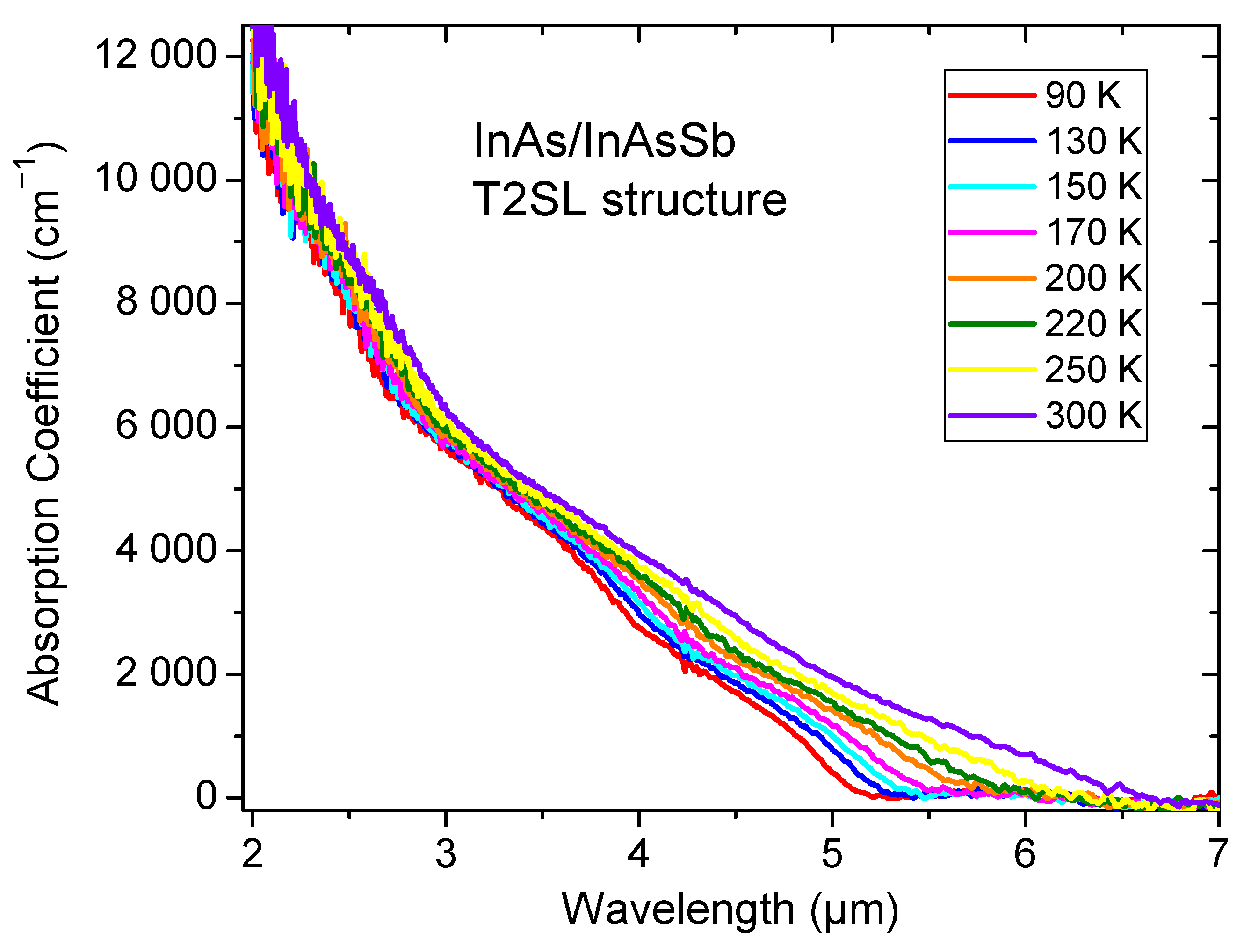
3.1. Absorption, Photoluminescence and Time-Resolved Photoluminescence Measurements

Figure 2 shows the absorption coefficient for temperature ranging from 90 K to 220 K. At λ = 3.4 µm, the absorption coefficient α reaches 4800 cm−1 at 150 K, in agreement with other values reported elsewhere [7,20,28]. The absorption band edge shows a wavelength red-shift with increasing temperature, while the absorption value remains relatively constant.
PL spectra, presented in Figure 3, display a shift in PL peak from 4.89 µm to 5.70 µm in the temperature range (77–250 K). Such values confirm that the Ga-free T2SL structure is relevant for the MWIR spectral domain.
The T2SL’s bandgap energy, extracted from the PL peak, as a function of temperature (Eg(T)) is shown in the inset of Figure 3, and a fitting curve (solid line) was plotted using the Einstein Oscillator model [8] through the equation Eg(T) = E0 – α × (TE/(exp(TE/T) − 1)), where α = 2.013 × 10⁻⁴ meV/K stands for the slope of the high-temperature linear asymptote, E0 = 258 meV stands for the energy gap at T = 0 K, TE = 117.6 K stands for the Einstein temperature and T is the absolute temperature. This fitting of the bandgap as a function of temperature will be used to analyze dark current density measurements performed on devices (see Section 3.3).
TRPL measurements were performed on the XBn T2SL structure (Figure 1b) to determine the minority carrier lifetime as a function of temperature (Figure 4). A lifetime value of 1 µs was extracted from these measurements for temperature ranging from 90 K to 220 K. As a consequence, since this value remains constant in this range of temperature, the minority carrier lifetime is limited by SRH processes [35]. Moreover, a lifetime value as high as 1 µs at 150 K validates the MBE growth of the Ga-free XBn InAs/InAs0.63Sb0.37 T2SL structure sample ready for device processing.

3.2. Quantum Efficiency Measurements

Figure 5a,b displays the QE as a function of temperature for two operating bias voltages Vb equal to −0.2 V and −0.4 V, respectively. The detector cut-off wavelength is 5 µm at 150 K, and a QE value higher than 50% is extracted (without anti-reflection coating (ARC)), which is a remarkable value considering the absorption coefficient and the low hole mobility in the T2SL structure [31,32]. Nevertheless, it may be observed that the QE values are strongly dependent on the applied voltage in the considered temperature range (77–220 K).
For Vb = −0.2V, we can observe (Figure 5a) that the 50% QE value is not reached for temperatures below 200 K. This may be due to the presence of an unwanted valence band offset (VBO) between the AL and BL which impedes the transport of hole minority carriers. This is not the case for Vb = −0.4V (Figure 5b), where this barrier seems to be overcome, resulting in higher QE values at low temperatures before saturation at 200 K.
Figure 6 displays the QE values measured at λ = 3.4 µm for different applied biases in the temperature range (77–220 K). The QE increases from 32% at T = 77 K and Vb = −0.4 V to reach 54% at T = 200–220 K and Vb = −0.3 V. This evolution with temperature is due to an increase in the hole minority carrier vertical diffusion length (along the growth axis), since absorption and lifetime measurements (Figure 2 and Figure 4, respectively) showed no significant evolution in this temperature range. Moreover, a slope of the QE can be observed, mainly at low temperature. This slope is a signature of a non-optimized device in the considered range of temperature. Indeed, if the AL thickness is longer than the vertical diffusion length of the minority carriers, some of the photo-generated carriers recombine before reaching the CL. Thus, an increase in the depletion width with the bias is necessary to promote the full collection of minority carriers. However, the QE begins to saturate at high temperature (Figure 6). Indeed, taking into account minority carrier lifetime and mobility values in the Ga-free T2SL structure [32], the vertical diffusion length increases with the temperature, allowing better collection of photo-generated carriers. At 150 K, a slight QE slope remains, while at 220 K, the QE completely saturates for biases lower than the operating bias (Vb= −0.4 V). A QE value higher than 55% highlights that the transport of hole minority carriers is optimized at this temperature, but not completely at the 150 K targeted temperature operation. Indeed, at this temperature, the hole vertical diffusion length was estimated at around 3 µm [32], in agreement with the chosen AL thickness.

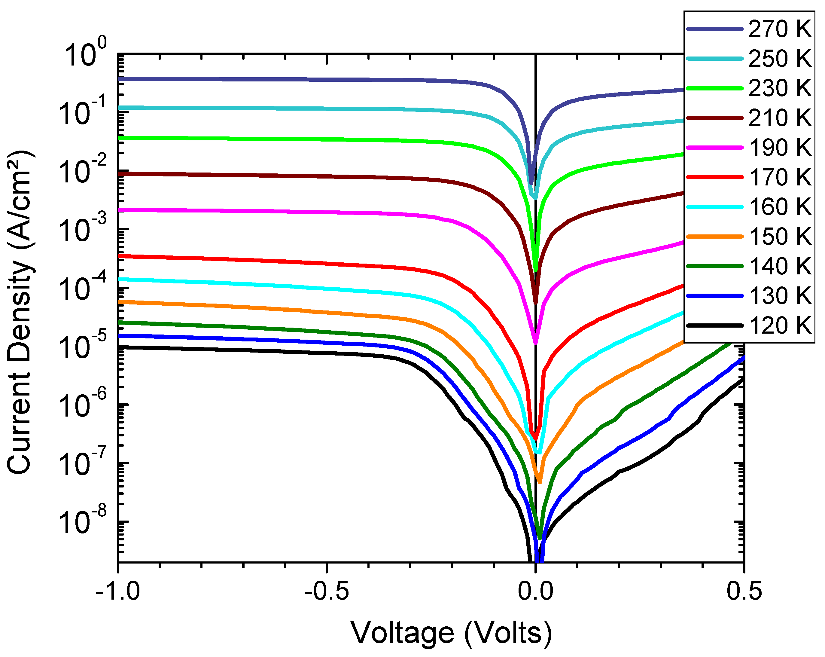
3.3. Dark Current–Voltage and Capacitance–Voltage Measurements

Figure 7 shows typical J-V characteristics carried out for a 210 µm diameter detector in the temperature range (120–270 K). At the 150 K targeted temperature operation, dark current density as low as 3.5 × 10⁻⁵ A/cm2 is recorded. Such a result must be improved, since when compared to the MCT state-of-the-art photodiode limited by diffusion dark current [36], the current is 20 times higher at the corresponding cut-off wavelength. Nevertheless, this value remains in agreement with the most recent results reported on Ga-free T2SL detectors [14,15,17,18,19,20,21].
From the dark J-V characteristics, transport regimes in the barrier detector can be identified by plotting the dynamic resistance area product RdA = (δJ/δV)−1, where A is the area of the device (210 µm diameter). Through the shape of the displayed curves in Figure 8, we can identify the main dark current regimes and analyze the QE spectra recorded (Figure 5).
The first significant bias value is the turn-on voltage (Von). This bias is located at the first RdA minimum and its value decreases when the temperature increases, from 260 mV to 85 mV in the temperature range (130–210 K). Below Von, the minority carriers are blocked due to the presence of the VBO in addition to the possible potential barrier due to the difference in doping between AL and CL. Above the reverse bias Von, the minority carriers can flow unimpeded through the barrier detector, and the quantum efficiency value becomes higher than 80% of its maximum value (Figure 6). We can remark that the higher the temperature, the lower the required voltage.
Next, the device reaches the operating voltage Vop. It is defined as the bias at which the maximum RdA product is obtained and is linked to the photoresponse spectra. At this particular Vop bias, the photonic current/quantum efficiency begins to saturate (Figure 6). At the targeted temperature of 150 K, Vop = −400 mV and the corresponding RdA product is equal to 2.5 × 10⁴ Ω.cm2 (Figure 8). Then, over Vop, the next visible RdA minimum VGR indicates the beginning of the generation–recombination (GR) regime. At this bias, the barrier is fully depleted and the depletion region expands into the absorber, which explains the appearance of the electric field-related GR current. Such behavior is only observed at low temperature since the device is diffusion current-limited for temperatures higher than 170 K.
Finally, extracted from J-V curves of Figure 7, dark current densities at Vop = −400 mV are reported as a function of 1/kBT (Arrhenius plot) in Figure 9, where kB is the Boltzmann constant.
A fit over the temperature range (150–270 K) using the expression A exp(–Ea/kB T) yields an activation energy Ea = 230 meV, which is approximately the T2SL energy bandgap (Eg) in this temperature range, signature of a diffusion-limited behavior. In the temperature range (120–150 K), the activation energy is 117 meV, approximately one half of the T2SL bandgap (Eg/2), indicating that the dark current is GR-limited, due to the presence of a depletion region extending into the AL.
To determine residual carrier concentrations, both in the nid p-type BL (Pres) and n-type AL (Nres), C-V measurements were performed [18]. From these measurements, a typical 1/C2 curve as a function of voltage at T = 150 K is shown in Figure 10. For biases below Von, the extracted slope leads to Pres = 2.7 × 1016 cm−3 in the BL while the slope at higher reverse voltage,(above the operating voltage Vop) leads to Nres = 3.2 × 1015 cm−3 in the AL. The residual doping, one order of magnitude higher in the BL, induces the presence of the electric field in the AL, even when no bias is applied.

4. Conclusions

The temperature dependence performances of MWIR Ga-free T2SL barrier photodetector have been reported.
At the expected temperature operation (T = 150 K), the quantum efficiency of the device, with no ARC, as high as 50% was achieved, but it is necessary to apply −400 mV (Vop) to reach this QE value. This means that there is a valence band barrier blocking the minority heavy hole carriers remaining at the AL/BL interface. A dark current density of the device as low as 3.5 × 10⁻⁵ A/cm2 was recorded. This result is on par with the state of the art, but the Arrhenius plot extracted from J-V measurements as a function of temperature shows that at temperatures lower than 150 K, the device is GR-limited, evidencing the presence of an unwanted electric field in the T2SL AL. Such a presence is consistent with C-V measurements showing higher residual doping in the BL.
The results obtained in this study highlight that the main problems are the presence of the electric field in the AL and a valence band offset at the BL–AL interface impeding the flow of minority carriers. To overcome these problems, a study of the AlAsSb BL must be conducted in terms of doping, thickness layer and alloy composition. This will be the subject of forthcoming investigations.

Author Contributions

M.B. and J.-P.P. fabricated the structures and devices; M.B., A.R. and V.A. performed the measurements; M.B., A.R., V.A., J.-P.P., I.R.-M., N.P.-L. and P.C. analyzed the data; M.B. and P.C. wrote the paper. All authors have read and agreed to the published version of the manuscript.

Funding

This work was partially funded by the French “Investment for the Future” program (EquipEx EXTRA, ANR 11-EQPX-0016) and by the French ANR under project HOT-MWIR (ANR-18-CE24-0019-01).

Institutional Review Board Statement

Not applicable.

Informed Consent Statement

Not applicable.

Data Availability Statement

The data that support the findings of this study are available from the corresponding author upon reasonable request.

Conflicts of Interest

The authors declare no conflict of interest.

References

  1. Klipstein, P. “XBn” barrier photodetectors for high sensitivity and high operating temperature infrared sensors. In Proceedings of the SPIE Defense and Security Conference, Orlando, FL, USA, 16–20 March 2008; Volume 6940, p. 69402U. [Google Scholar]
  2. Ting, D.Z.; Rafol, S.B.; Khoshakhlagh, A.; Keo, S.A.; Soibel, A.; Fisher, A.M.; Pepper, B.J.; Hill, C.J.; Gunapala, S.D.; Pagano, T.S. Type-II Superlattice Mid-Wavelength Infrared Focal Plane Arrays for CubeSat Hyperspectral Imaging. IEEE Photon. Technol. Lett. 2022, 34, 329–332. [Google Scholar] [CrossRef]
  3. Steenbergen, E.H.; Nunna, K.; Ouyang, L.; Ullrich, B.; Huffaker, D.L.; Smith, D.J.; Zhang, Y.-H. Strain-balanced InAs/InAsSb type-II superlattices grown by molecular beam epitaxy on GaSb substrates. J. Vac. Sci. Technol. 2012, 30, 02B107. [Google Scholar] [CrossRef]
  4. Lackner, D.; Steger, M.; Thewalt, M.L.W.; Pitts, O.J.; Cherng, Y.T.; Watkins, S.P.; Plis, E.; Krishna, S. InAs/InAsSb strain balanced superlattices for optical detectors:Material properties and energy band simulations. J. Appl. Phys. 2012, 111, 034507. [Google Scholar] [CrossRef]
  5. Olson, B.V.; Shaner, E.A.; Kim, J.K.; Klem, J.F.; Hawkins, S.D.; Murray, L.M.; Prineas, J.P.; Flatté, M.E.; Boggess, T.F. Time-resolved optical measurements of minority carrier recombination in a midwave infrared InAsSb alloy and InAs/InAsSb superlattice. Appl. Phys. Lett. 2012, 101, 092109. [Google Scholar] [CrossRef]
  6. Schuler-Sandy, T.; Klein, B.; Casias, L.; Mathews, S.; Kadlec, C.; Tian, Z.; Plis, E.; Myers, S.; Krishna, S. Growth of InAs–InAsSb SLS through the use of digital alloys. J. Cryst. Growth 2015, 425, 29–32. [Google Scholar] [CrossRef]
  7. Webster, P.T.; Riordan, N.A.; Liu, S.; Steenbergen, E.H.; Synowicki, R.A.; Zhang, Y.-H.; Johnson, S.R. Absorption properties of type-II InAs/InAsSb superlattices measured by spectroscopic ellipsometry. Appl. Phys. Lett. 2015, 106, 061907. [Google Scholar] [CrossRef] [Green Version]
  8. Webster, P.T.; Riordan, N.A.; Liu, S.; Steenbergen, E.H.; Synowicki, R.A.; Zhang, Y.-H.; Johnson, S.R. Measurement of InAsSb bandgap energy and InAs/InAsSb band edge positions using spectroscopic ellipsometry and photoluminescence spectroscopy. J. Appl. Phys. 2015, 118, 245706. [Google Scholar] [CrossRef] [Green Version]
  9. Haugan, H.J.; Mahalingam, K.; Szmulowicz, F.; Brown, G.J. Quantitative study of the effect of deposition temperature on antimony incorporation in InAs/InAsSb superlattices. J. Crystal Growth 2016, 436, 134–137. [Google Scholar] [CrossRef]
  10. Lu, J.; Luna, E.; Aoki, T.; Steenbergen, E.H.; Zhang, Y.-H.; Smith, D.J. Evaluation of antimony segregation in InAs/InAsSb type-II superlattices grown by molecular beam epitaxy. J. Appl. Phys. 2016, 119, 095702. [Google Scholar] [CrossRef] [Green Version]
  11. Durlin, Q.; Perez, J.P.; Rossignol, R.; Rodriguez, J.B.; Cerutti, L.; Delacourt, B.; Rothman, J.; Cervera, C.; Christol, P. InAs/InAsSb superlattice structure tailored for detection of the full midwave infrared spectral domain. In Proceedings of the SPIE Quantum Sensing and Nano Electronics and Photonics XIV, San Francisco, CA, USA, 29 January–2 February 2017; Volume 10111, p. 1011112. [Google Scholar]
  12. Rhiger, D.; Smith, E.P.; Kolosa, B.P.; Kim, J.K.; Klem, J.F.; Hawkins, S.D. Analysis of III–V Superlattice nBn Device Characteristics. J. Electron. Mater. 2016, 45, 4646–4653. [Google Scholar] [CrossRef]
  13. Ting, D.Z.; Soibel, A.; Khoshakhlagh, A.; Rafol, S.B.; Keo, S.A.; Höglund, L.; Fisher, A.M.; Luong, E.M.; Gunapala, S.D. Mid-wavelength high operating temperature barrier infrared detector and focal plane array. Appl. Phys. Lett. 2018, 113, 021101. [Google Scholar] [CrossRef]
  14. Soibel, A.; Ting, D.Z.; Rafol, S.B.; Fisher, A.M.; Keo, S.A.; Khoshakhlagh, A.; Gunapala, S.D. Mid-wavelength infrared InAsSb/InAs nBn detectors and FPAs with very low dark current density. Appl. Phys. Lett. 2019, 114, 161103. [Google Scholar] [CrossRef]
  15. Michalczewski, K.; Tsai, T.Y.; Martyniuk, P.; Wu, C.H. Demonstration of HOT photoresponse of MWIR T2SLs InAs/InAsSb photoresistors. Bull. Pol. Acad. Sci. Tech. Sci. 2019, 67, 141–145. [Google Scholar]
  16. Rhiger, D.; Smith, E.P. Carrier transport in the valence band of nBn III–V superlattice infrared detectors. J. Electron. Mater. 2019, 48, 6053–6062. [Google Scholar] [CrossRef] [Green Version]
  17. Wu, D.; Li, J.; Dehzangi, A.; Razeghi, M. Mid-wavelength infrared high operating temperature pBn photodetectors based on type-II InAs/InAsSb superlattice. AIP Adv. 2020, 10, 025018. [Google Scholar] [CrossRef] [Green Version]
  18. Zavala-Moran, U.; Bouschet, M.; Perez, J.P.; Alchaar, R.; Bernhardt, S.; Ribet-Mohamed, I.; De Anda-Salazar, F.; Christol, P. Structural, optical and electrical characterizations of midwave infrared Ga-free Type-II InAs/InAsSb superlattice barrier photodetector. Photonics 2020, 7, 76. [Google Scholar] [CrossRef]
  19. Wu, D.; Li, J.; Dehzangi, A.; Razeghi, M. High performance InAs/InAsSb Type-II superlattice mid-wavelength infrared photodetectors with double barrier. Inf. Phys. Technol. 2020, 109, 103439. [Google Scholar] [CrossRef]
  20. Soibel, A.; Ting, D.Z.; Fisher, A.M.; Khoshakhlagh, A.; Pepper, B.; Gunapala, S.D. Temperature dependence of diffusion length and mobility in mid-wavelength InAs/InAsSb superlattice infrared detectors. Appl. Phys. Lett. 2020, 117, 231103. [Google Scholar] [CrossRef]
  21. Dehzangi, A.; Wu, D.; McClintock, R.; Li, J.; Razeghi, M. Planar nBn type-II superlattice mid-wavelength infrared photodetectors using zinc ion-implantation. Appl. Phys. Lett. 2020, 116, 221103. [Google Scholar] [CrossRef]
  22. Bouschet, M.; Zavala-Moran, U.; Arounassalame, V.; Alchaar, R.; Bataillon, C.; Ribet-Mohamed, I.; De Anda-Salazar, F.; Perez, J.P.; Péré-Laperne, N.; Christol, P. Influence of pixel etching on electrical and electro-optical performances of a Ga-free InAs/InAsSb T2SL barrier photodetector for mid-wave infarred imaging. Photonics 2021, 8, 194. [Google Scholar] [CrossRef]
  23. She, L.; Jiang, J.; Chen, W.; Cui, S.; Jiang, D.; Wang, G.; Xu, Y.; Hao, H.; Wu, D.; Ding, Y.; et al. Mid-wave infrared p+-B-n InAs/InAsSb type-II superlattice photodetector with an AlAsSb/InAsSb superlattice barrier. Inf. Phys. Technol. 2022, 121, 104015. [Google Scholar] [CrossRef]
  24. Ariyawansa, G.; Joshua Duran, J.; Reyner, C.; Scheihing, J. InAs/InAsSb strained-layer superlattice mid-wavelength infrared detector for high-temperature operation. Micromachines 2019, 10, 806. [Google Scholar] [CrossRef] [Green Version]
  25. Deng, G.; Chen, D.; Yang, S.; Yang, C.; Yuan, J.; Yang, W.; Zhang, Y. High operating temperature pBn barrier mid-wavelength infrared photodetectors and focal plane array based on InAs/InAsSb strained-layer superlattices. Opt. Express 2020, 28, 17611–17619. [Google Scholar] [CrossRef]
  26. Ting, D.Z.; Rafol, S.B.; Keo, S.A.; Nguyen, J.; Khoshakhlagh, A.; Soibel, A.; Höglund, L.; Fisher, A.M.; Luong, E.M.; Mumolo, J.M.; et al. InAs/InASb Type-II superlattice mid-wavelength infrared focal plane array with significantly higher operating temperature than InSb. IEEE Photonics J. 2018, 10, 6804106. [Google Scholar] [CrossRef]
  27. Klipstein, P.C. Perspective on III–V barrier detectors. Appl. Phys. Lett. 2002, 120, 060502. [Google Scholar] [CrossRef]
  28. Rhiger, D.; Smith, E.P. Infrared absorption near the bandgap in the InAs/InAsSb superlattice. In Proceedings of the SPIE Infrared Sensors, Devices, and Applications X, Online, 9 September 2020; Volume 11503, p. 1150305. [Google Scholar]
  29. Krizman, G.; Carosella, F.; Bermejo-Ortiz, J.; Philippe, A.; Rodriguez, J.-B.; Perez, J.-P.; Christol, P.; de Vaulchier, L.-A.; Guldner, Y. Magneto-spectroscopy investigation of InAs/InAsSb superlattices for midwave infrared detection. J. Appl. Phys. 2021, 130, 055704. [Google Scholar] [CrossRef]
  30. Tsai, C.-Y.; Zhang, Y.; Ju, Z.; Zhang, Y.-H. Study of vertical hole transport in InAs/InAsSb type-II superlattices by steady-state and time-resolved photoluminescence spectroscopy. Appl. Phys. Lett. 2020, 116, 201108. [Google Scholar] [CrossRef]
  31. Casias, L.K.; Morath, C.P.; Steenbergen, E.H.; Umana-Membreno, G.A.; Webster, P.T.; Logan, J.V.; Kim, J.K.; Balakrishnan, G.; Faraone, L.; Krishna, S. Vertical carrier transport in strain-balanced InAs/InAsSb type-II superlattice material. Appl. Phys. Lett. 2020, 116, 182109. [Google Scholar] [CrossRef]
  32. Arounassalame, V.; Bouschet, M.; Alchaar, R.; Ferreira, R.; Carosella, F.; Ramiandrasoa, A.; Perez, J.-P.; Péré-Laperne, N.; Christol, P.; Ribet-Mohamed, I. Anisotropic transport investigation through different etching depths in InAs/InAsSb T2SL barrier midwave infrared detector. Inf. Phys. Technol. 2022, 126, 104315. [Google Scholar] [CrossRef]
  33. Donetsky, D.; Belenky, G.; Svensson, S.; Suchalkin, S. Minority carrier lifetime in type-II InAs/GaSb strained-layer superlattices and bulk HgCdTe materials. Appl. Phys. Lett. 2010, 97, 052108. [Google Scholar]
  34. Giard, E.; Taalat, R.; Delmas, M.; Rodriguez, J.-B.; Christol, P.; Ribet-Mohamed, I. Radiometric and noise characteristics of InAs-rich T2SL MWIR pin photodiodes. J. Eur. Opt. Soc. Rapid Publ. 2014, 9, 14022. [Google Scholar] [CrossRef] [Green Version]
  35. Olson, B.B.; Shaner, E.; Kim, J.; Klem, J.; Hawkins, S.; Flatté, M.; Boggess, T. Identification of dominant recombination mechanisms in narrow-bandgap inas/inassb type-II superlattices and InAsSb alloys. Appl. Phys. Lett. 2013, 103, 052106. [Google Scholar] [CrossRef]
  36. Tennant, W.E.; Lee, D.; Zandian, M.; Piquette, E.; Carmody, M. MBE HgCdTe technology: A very general solution to IR detection, described by “Rule 07”, a very convenient heuristic. J. Electron. Mater. 2008, 37, 1406–1410. [Google Scholar] [CrossRef]
Figure 1. Schematic view of the different epilayers stacking under study. (a) T2SL structure used for absorption and photoluminescence measurements. (b) XBn detector structure used for lifetime, dark current, capacitance–voltage and quantum efficiency measurements.
Applsci 12 10358 g001
Figure 2. Absorption coefficient versus wavelength of InAs (4.17 nm)/InAsSb (1.42 nm) T2SL at various temperatures.
Applsci 12 10358 g002
Figure 3. PL spectra of the Ga-free InAs/InAs0.63Sb0.37 T2SL structure between 28 K and 250 K. Inset shows the temperature dependence of the T2SL’s bandgap where the solid line is a fit curve using Einstein oscillator’s equation.
Applsci 12 10358 g003
Figure 4. TRPL signal of the Ga-free XBn InAs/InAs0.63Sb0.37 T2SL structure at 80 K, 150 K and 250 K. Inset shows the minority carrier lifetime values extracted from measurements.
Applsci 12 10358 g004
Figure 5. Front side illuminated spectral quantum efficiency taken at different temperatures (from 77 K to 220 K) and under two biases, Vb = −0.2 V (a) and Vb = −0.4 V (b).
Applsci 12 10358 g005
Figure 6. Quantum efficiency measured at λ = 3.4 µm as a function of the applied bias voltages for various detectors’ temperatures.
Applsci 12 10358 g006
Figure 7. Dark current density characteristics of XBn InAs/InAsSb T2SL detector at different temperatures from 120 K to 270 K.
Applsci 12 10358 g007
Figure 8. Differential resistance area (RdA) product as a function of the voltage for various detectors’ temperature. Positions of relevant voltages (Von, Vop, VGR) are identified (dotted line).
Applsci 12 10358 g008
Figure 9. Arrhenius plot extracted from J-V curves in dark conditions at Vop = −400 mV. Diffusion and generation–recombination dark current regimes are clearly identified.
Applsci 12 10358 g009
Figure 10. The 1/C2(V) characteristic extracted from C-V measurement at T = 150 K.
Applsci 12 10358 g010
Publisher’s Note: MDPI stays neutral with regard to jurisdictional claims in published maps and institutional affiliations.

