Article

Complementary Barrier Infrared Detector Architecture for Long-Wavelength Infrared InAs/InAsSb Type-II Superlattice

NASA Jet Propulsion Laboratory, California Institute of Technology, Pasadena, CA 91109-8099, USA
*
Author to whom correspondence should be addressed.
Appl. Sci. 2022, 12(24), 12508; https://doi.org/10.3390/app122412508
Submission received: 20 October 2022 / Revised: 29 November 2022 / Accepted: 30 November 2022 / Published: 7 December 2022
(This article belongs to the Special Issue Design and Study of Type-2 Superlattice Photodetectors)

Abstract

:
We describe the challenges for long- and very long-wavelength InAs/InAsSb type-II strained-layer superlattice infrared detectors, and provide an overview of progress in device architecture development for addressing them. Specifically, we have explored the complementary barrier infrared detector (CBIRD) that contains p-type InAs/InAsSb T2SLS absorbers for enhancing quantum efficiency, while also suppressing surface shunt current. We describe selected device results, and also provide references to additional results and more in-depth discussions.

1. Introduction

III–V semiconductor infrared focal plane arrays (FPAs) are known for their spatial uniformity, temporal stability, high operability, and affordability. Compared to bulk III–V semiconductor infrared photodiodes, III–V semiconductor type-II superlattice (T2SL) infrared detectors have wide-range cutoff wavelength adjustability, suppressed band-to-band tunneling [1], and reduced Auger recombination [2]. The InAs/Ga(In)Sb T2SL is well established as an infrared detector material, and has been described in detail in review articles [3,4,5]. The InAs/InAsSb (Gallium-free) type-II strained-layer superlattice (T2SLS) has emerged in recent years as an important infrared photodetector material also. Compared to the InAs/Ga(In)Sb T2SL, the InAs/InAsSb T2SLS is easier to grow, and has longer minority carrier lifetimes [6,7,8,9,10]. In the mid-wavelength infrared (MWIR) InAs/InAsSb, T2SLS FPA based on the nBn detector architecture [11] has demonstrated a 40–50 K operating temperature advantage over the market-leading InSb FPA, while retaining III-V semiconductor advantages such as affordability, uniformity, and high operability [12,13]. However, compared to the InAs/Ga(In)Sb T2SL, the InAs/InAsSb T2SLS also has some disadvantages; this makes extension to the long-wavelength infrared (LWIR) and very long-wavelength infrared (VLWIR) with good detector performance challenging. For our purposes, we take MWIR as 3–8 µm, LWIR as 8–12 µm, and VLWIR as >12 µm. In this paper, we present an overview of progress in (V)LWIR device architecture development at the NASA Jet Propulsion Laboratory (JPL), and provide additional references to more in-depth discussions. In Section 2, we discuss the (V)LWIR challenges for the InAs/InAsSb T2SLS. Section 3 describes detector architecture for addressing some of these challenges. Section 4 reports selected device results. Section 5 concludes with a discussion.

2. Challenges for (V)LWIR InAs/InAsSb T2SLS Detectors

In this section, we provide an overview of the challenges for (V)LWIR InAs/InAsSb T2SLS detectors due to (1) superlattice bulk properties and (2) InAs/InAsSb superlattice surface properties.

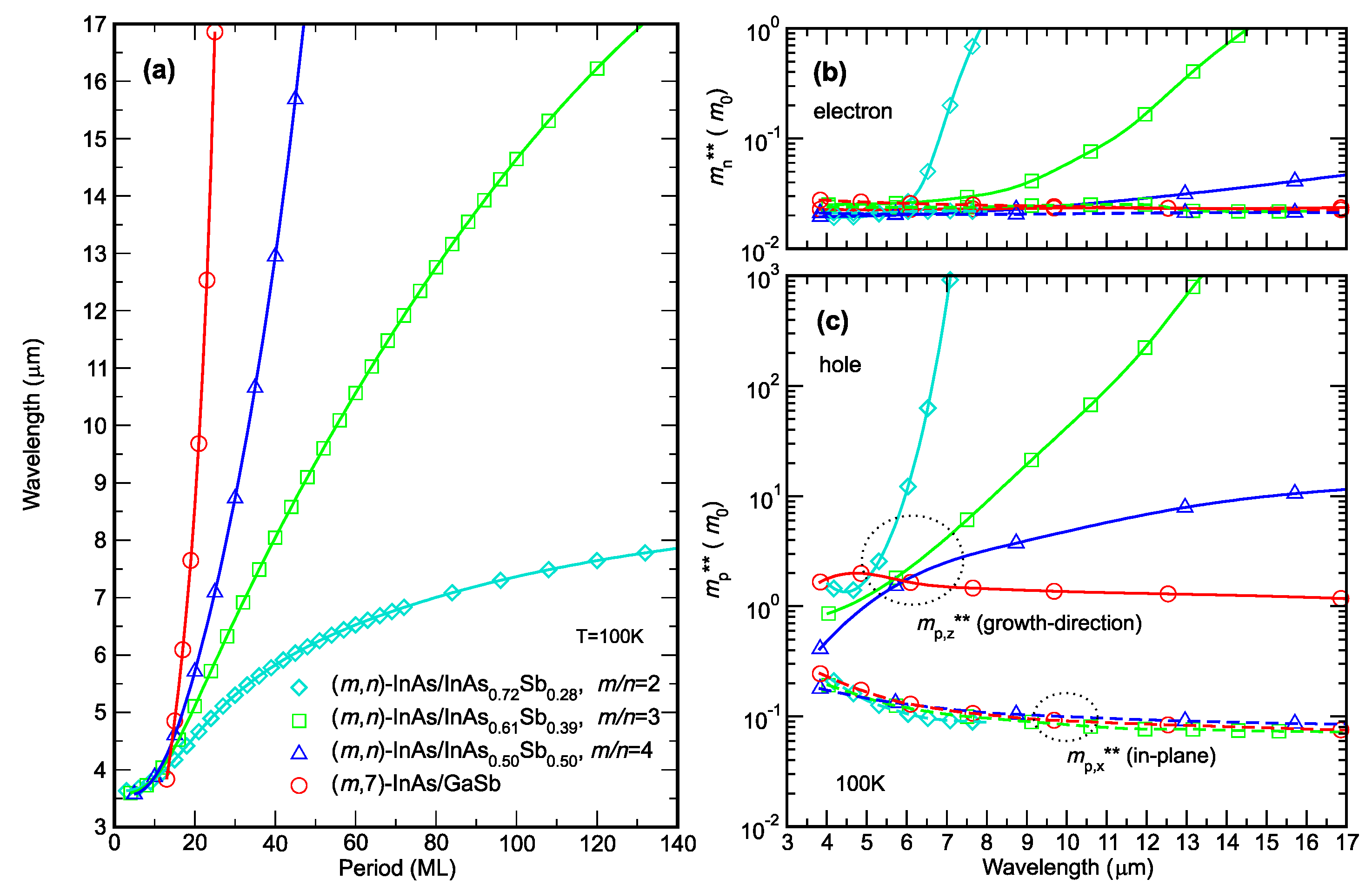
2.1. Challenges Related to (V)LWIR InAs/InAsSb T2SLS Bulk Properties

Two intrinsic properties of bulk InAs/InAsSb T2SLS present challenges for achieving good quantum efficiency (QE) in the (V)LWIR. First, InAs/InAsSb T2SLS has weaker absorption than the InAs/GaSb T2SL in the (V)LWIR [14,15], and therefore requires a thicker absorber layer to achieve comparable QE. Second, (V)LWIR InAs/InAsSb T2SLS has a short hole diffusion length, which affects devices that make use of n-type absorbers. We discuss these two issues in more detail below. An in-depth theoretical discussion on the challenges for (V)LWIR InAs/InAsSb T2SLS can be found in [16].
The smaller absorption coefficients of (V)LWIR InAs/InAsSb T2SLS can be traced to the fact that a longer superlattice period is required to achieve the same band gap (or equivalently the corresponding detector cutoff wavelength) than the InAs/GaSb T2SL. In a type-II superlattice, the band-edge electron and hole wavefunctions are localized in different layers. In the case of InAs/InAsSb, the lowest conduction sub-band wavefunction is in the InAs layers, while the highest valence sub-band wavefunction is in the InAsSb layers. Longer superlattice period leads to smaller electron–hole wavefunction overlap and weaker absorption coefficient. Therefore, the period required to reach a given band gap (Eg), or the corresponding cutoff wavelength (assumed as λcutoff = hc/Eg), is a simple but often informative quantity for a type-II superlattice. We used an enhanced effective bond orbital model (EBOM) [17,18,19] to calculate the superlattice band gap. Figure 1a shows the calculated cutoff wavelength as a function of superlattice period for three sets of (m,n)-InAs/InAsSb T2SLS (m and n respectively being the number of monolayers of InAs and InAsSb in each superlattice period) with different m/n ratios. The results for a set of (m,n)-InAs/GaSb T2SL with n = 7 are also plotted for comparison. The cutoff wavelength is derived from the calculated superlattice band gap using the relationship λcutoff [µm] = 1.24/Eg [eV]. For the InAs/InAsSb T2SLS, the InAsSb alloy composition for a family with a given m/n ratio is chosen to achieve strain balance with respect to the GaSb substrate; higher m/n ratio is associated with InAsSb alloy with higher Sb concentration (which is more compressively strained with respect to the GaSb substrate).
Figure 1a shows that InAs/InAsSb T2SLS with higher Sb fraction (larger m/n ratio) can reach a specified cutoff wavelength with shorter superlattice period, and is thus more favorable. Overall, in the MWIR range, all four sets of superlattices have fairly comparable periods. However, as the cutoff wavelength increases, the periodicity disadvantage of the InAs/InAsSb T2SLS with respect to the InAs/GaSb T2SL becomes more apparent, especially with lower Sb alloy fractions. This is one of the main challenges InAs/InAsSb T2SLS. We note that in Figure 1a, the highest InAsSb alloy Sb fraction that we used is 50%, and in principle, we can use InAs/InAsSb T2SLS with even higher Sb fractions. In fact, it has been shown that at an Sb fraction of 74%, the InAs/InAsSb T2SLS nearly matches the InAs/GaSb T2SL in the cutoff wavelength vs. superlattice period characteristics [16]. However, in practice, Sb segregation effects can negate the benefit of higher Sb fraction; see [16] for more detailed discussions.
The short hole diffusion length in (V)LWIR InAs/InAsSb T2SLS can be traced to the large hole conductivity effective mass along the growth direction. From the expressions for diffusion length ( L = D τ r ), diffusivity ( D = μ k B T / e ), and mobility ( μ = e τ c / m * * ) we can write the diffusion length along the ith direction as L i = [ ( k B T / m i * * ) τ r τ c , i ] 1 / 2 , where the roles of the conductivity effective mass m i * * , the minority carrier recombination lifetime τ r , and the collision (momentum relaxation) time τ c , i are delineated. It can be seen that larger conductivity effective mass leads to shorter diffusion length. We note that the conductivity effective mass differs from the band-edge curvature effective mass, and we therefore use a “double-starred” notation to emphasize the distinction between the conductivity effective mass and the band-edge curvature effective mass (typically with “single-starred” notation). The conductivity effective mass is a thermally averaged quantity that accounts for the anisotropy and non-parabolicity in the superlattice band structure, and is given, approximately, by the expression m i * * k B T / v i 2 , where v i is the band structure-derived group velocity along the ith direction. Detailed discussions on the conductivity effective mass are found in [20,21].
Figure 1b shows the calculated electron conductivity effective masses along the growth direction z (mn,z**) and the in-plane direction x (mn,x**) as functions of cutoff wavelengths for the same sets of superlattices, discussed in Figure 1a; Figure 1c shows the corresponding hole conductivity effective masses mp,z** and mp,x**. The numerical values of the various conductivity effective masses for a 5.7 µm cutoff and a 13 µm cutoff (m,n)-InAs/InAs0.5Sb0.5 T2SLS, (m/n) = 4, are tabulated in Table 1. In general, for the cutoff wavelength range shown in Figure 1, the electron conductivity effective mass mn,z** is quite small in InAs/InAsSb T2SLS with higher (~50%) Sb fraction since the wavefunctions of the lowest conduction sub-bands are only weakly confined in the relative shallow conduction band quantum wells. On the other hand, the hole conductivity effective mass mp,z** can be very large in the (V)LWIR superlattices where the InAsSb hole quantum wells are separated by wider InAs layer. Here, a higher Sb fraction reduces the InAs/InAsSb T2SLS period, and is therefore helpful in reducing the value of mp,z**. Nevertheless, for the InAs/InAsSb T2SLS, mp,z** can still be more than two orders of magnitude greater than mn,z** in the (V)LWIR, even with 50% Sb (see Table 1). Therefore, we expect the hole diffusion length to be much shorter than the electron diffusion length for (V)LWIR InAs/InAsSb T2SLS.
Another important aspect shown in Figure 1 is superlattice conductivity effective masses anisotropy. Figure 1b shows that while the growth direction and in-plane electron conductivity effective masses, mn,z** and mn,x**, respectively, are very similar at below 6 µm cutoff wavelength (λc), they begin to diverge as the cutoff wavelength increases. However, in InAs/InAsSb T2SLS with higher (~50%) Sb fraction, this difference between mn,z** and mn,x** can be kept reasonably small, even at λc = 13 µm (see Table 1). Therefore, electron conductivity effective mass anisotropy can be manageable. The picture is quite different for hole conductivity effective masses. As shown in Figure 1c, the difference between mp,z** and mp,x** for the InAs/InAsSb T2SLS is already very significant in the MWIR, and continues to grow as the cutoff wavelength increases. This anisotropy is greater for InAs/InAsSb T2SLS with lower Sb fraction alloys. However, even for the best case shown (InAs/InAsSb T2SLS with 50% Sb fraction) in Figure 1c, the (mp,z**/mp,x**) ratio is 11.5 at λc = 5.7 µm, and increases to 86.8 at λc = 13 µm (See Table 1). The case for the (m,7)-InAs/GaSb T2SL is better, with the (mp,z**/mp,x**) ratio remaining at a relatively constant value of ~1 order of magnitude over the λc = 5 µm to 17 µm range. The large hole conductivity effective mass anisotropy leads to hole mobility anisotropy. Having much larger in-plane than growth direction hole mobility can be very unfavorable from FPA crosstalk and modulation transfer function (MTF) considerations. This was explicitly demonstrated in the nBn FPA pixels simulations by Schuster [22]. We will provide additional comment on the crosstalk issue in Section 3, after describing our device architecture.
Here, we summarize the findings of this section. In the (V)LWIR, the InAs/InAsSb T2SLS has weaker absorption than the InAs/GaSb T2SL, and therefore requires a thicker absorber layer to achieve comparable QE. The growth direction hole conductivity effective mass of the (V)LWIR InAs/InAsSb T2SLS increases rapidly with cutoff wavelength, leading to low hole mobility and short hole diffusion length, which in turn limits the viable absorber thickness for n-type InAs/InAsSb T2SLS. In general, the attainable QE for (V)LWIR InAs/InAsSb T2SLS detectors with n-type absorber is limited, and also becomes progressively smaller as the cutoff wavelength increases. For the p-type superlattice absorbers, we can take advantage of the much smaller growth direction electron conductivity effective mass, and also the more favorable electron conductivity effective mass anisotropy characteristics. This suggests that we can address the (V)LWIR QE problem by using p-type absorbers, which provide higher mobility and longer diffusion lengths for minority carriers (electrons). It is worth noting that although the first published LWIR InAs/InAsSb T2SLS detector results [23] were for an nBn detector (with n-type absorber), earlier studies on LWIR InAs/GaSb T2SL detectors [24,25,26,27] mostly use p-type absorbers because of the well-known concerns for low growth direction hole mobility. The reason that the n-type (V)LWIR InAs/InAsSb T2SLS absorbers were considered at all was probably due to the success of the nBn detector architecture in general, and the success of the MWIR InAs/InAsSb T2SLS nBn detector in particular.

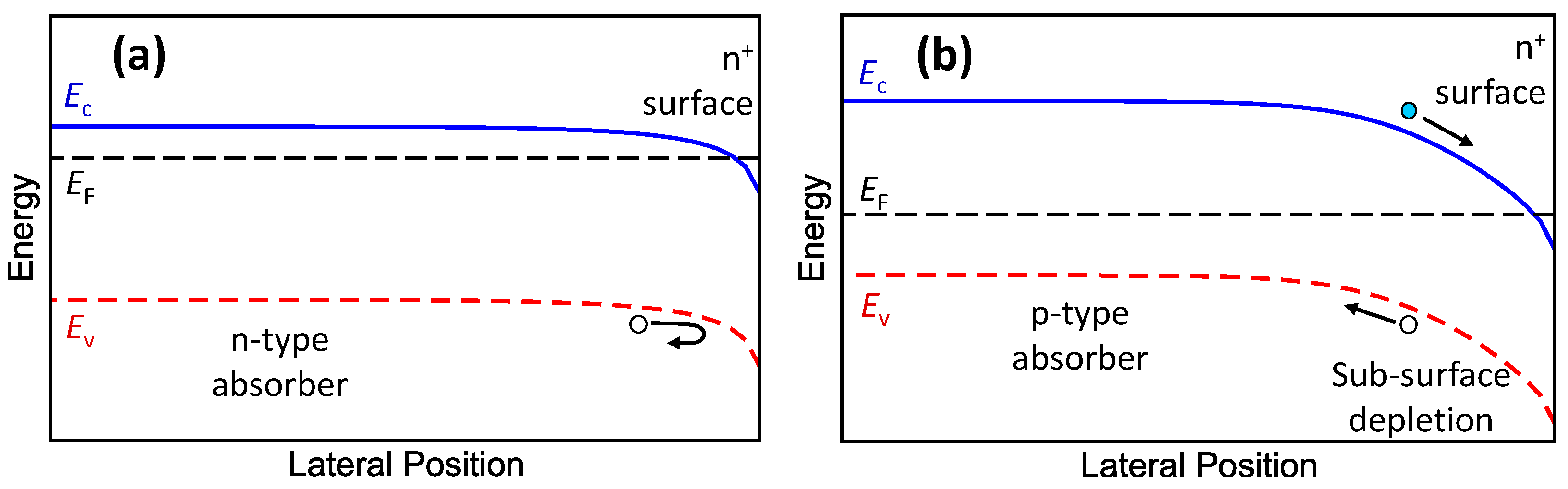
2.2. Challenges Related to InAs/InAsSb T2SLS Surface Properties

It has been known that the InAs surface Fermi level is actually above its conduction band edge, regardless of whether InAs is doped n-type or p-type [28,29]; the InAs surface inverts to n-type even if it is doped degenerate p-type [28]. For InAs/InAsSb T2SLS strain balanced on GaSb substrate, the typical net InAs fraction is ~90%, and therefore the surface of InAs/InAsSb T2SLS might be expected to show InAs-like behavior. Indeed, based on Schottky barrier height-derived band alignment data [30], and the calculated superlattice band edge positions [31], Sidor and co-workers concluded that both MWIR and LWIR InAs/InAsSb T2SLS surface Fermi levels are in the conduction band also [32].
In using p-type InAs/InAsSb T2SLS absorber for QE enhancement, we encounter two surface-related issues due to the fact that, regardless of doping type, the surface of the InAs/InAsSb T2SLS is always degenerate n-type. We provide a brief overview of these issues in this sub-section. Extensive discussions on surface related dark currents in antimonide-based detectors can be found in the references by Sidor, Savich, and Wicks [32,33].
We turn to p-type InAs/InAsSb T2SLS absorber for QE enhancement. The simplest p-type unipolar barrier detector structure is the pBp or the XBp [34,35]. The pBp is the analogue of the nBn, but with a p-type top contact, a unipolar hole barrier, and a p-type absorber. The layer structure of a pBp detector, along with that of an nBn detector, are illustrated in Figure 2. The pBp has been implemented successfully for (V)LWIR InAs/GaSb T2SL absorbers [36,37]. For the InAs/InAsSb T2SLS, there is an extra complication in that the surface of p-type InAs/InAsSb superlattice inverts to degenerate n-type. As illustrated in Figure 2b, the inverted surface provides a surface electron current path that is not blocked by the unipolar hole barrier, leading to electron surface leakage dark current (sidewall shunt current). We note from Figure 2a that the electron surface leakage path in the nBn is interrupted by the presence of the unipolar electron barrier, and therefore even for a fully reticulated nBn detector pixel, the sidewall shunt current is suppressed.
Another surface issue for the p-type absorber can be seen in Figure 3, where the energy band diagrams near the sidewall surface of n-type and p-type absorbers are illustrated. Figure 3a show that near the n-type absorber surface, the accumulated surface potential repels the minority carriers (holes) from the etched absorber surface, which consequently is relatively benign. However, for the p-type absorber, the surface band bending is problematic. As illustrated in Figure 3b, the degenerate n-type surface of the p-type absorber attracts minority carriers (electrons); the inverted surface also creates a surface pn junction with a sub-surface depletion region, and is subject to various surface dark current mechanisms [33,38].
The analysis in this sub-section shows that for the InAs/InAsSb T2SLS, the nBn or XBn [39,40] device architecture is robust against surface leakage and surface band bending; the only drawback is the limited (V)LWIR QE. On the other hand, the pBp can provide higher QE, but is subject to the electron surface leakage dark current, as well as surface-related dark current mechanisms associated with the surface pn junction. Incidentally, these same surface problems also affect the simple pn diode. Therefore, to make effective use of p-type, InAs/InAsSb T2SLS absorber for enhanced QE, alternative device architecture is needed.

3. The CBIRD Device Architecture

The complementary barrier infrared detector (CBIRD) is a non-equilibrium device [41,42,43], where, under reverse bias, the minority density is reduced to below equilibrium values through exclusion and extraction [44]. The CBIRD structure consists of an absorber surrounded on the two sides by a pair of complementary unipolar electron and hole barriers, and capped at the two ends with top and bottom contact layers. The CBIRD absorber can be n-type (n-CBIRD), p-type (p-CBIRD), or even a combination of p-type and n-type (pn-CBIRD). The CBIRD was originally implemented for p-type InAs/GaSb T2SL absorbers [45,46], but can be implemented readily for InAs/InAsSb T2SLS absorbers as well [47,48]. Figure 4 shows schematic layer diagrams for a set of generic n-CBIRD, p-CBIRD, and pn-CBIRD structures with InAs/InAsSb T2SLS absorbers. In each case, the etch-exposed absorber surface is degenerate n-type, but the electron surface leakage path is blocked by the unipolar electron barrier. We note that if the etch-exposed absorber surface is degenerate p-type, the hole surface leakage path would be similarly blocked by the unipolar hole barrier. The n-CBIRD illustrated in Figure 4a may be thought of as an nBn/XBn with a wide-gap emitter contact for reducing minority carrier injection. It has the same good dark current characteristics as the nBn/XBn, and is resilient with respect to surface issue as discussed in the last section. In the (V)LWIR, the attainable QE for n-CBIRD is limited by the short hole diffusion length. Absorber band gap grading, introduced by gradually varying the absorber superlattice period, can be used to create a built-in quasi-electric field that facilitates hole transport through drift in n-type absorber; this can provide a modest amount of QE enhancement. A more effective way to enhance QE is to take advantage of the thicker absorber afforded by the much longer electron diffusion length in the p-CBIRD, which is illustrated in Figure 4b. The drawback of the p-CBIRD is that it requires a deep etch through the p-type absorber and past the pn junction, as depicted in Figure 4b. The exposed sidewalls, which run over the entire length of the p-type absorber, is a source of surface-related dark currents unless good surface passivation can be implemented.
As an alternative to the p-CBIRD, we consider a CBIRD structure that incorporates both p-type and n-type absorber sections (pn-CBIRD) [47,48,49], as illustrated in Figure 4c. In the pn-CBIRD, a portion of the p-type absorber is replaced by an n-type absorber (for which the thickness is limited by the hole diffusion length). The n-type absorber can be either graded or non-graded. To delineated detector array pixels, we only need to etch past the absorber pn junction, as illustrated in Figure 4c. The shallower mesa etch in the pn-CBIRD reduces fabrication demands and also decreases the exposed surface area of the p-type absorber. A drawback of the pn-CBIRD compared to the p-CBIRD is that it contains a pn homojunction, which is a source of generation-recombination (G-R) and tunneling dark current.
In Section 2, we discussed how the anisotropy in superlattice hole conductivity effective mass could lead to FPA crosstalk and degraded MTF. If this issue is a concern for a pn-CBIRD FPA (e.g., FPA with smaller pixel pitch), we could choose to fully reticulate the pn-CBIRD pixels. This would expose the sidewalls of the n-type absorber section of the pn-CBIRD. However, as discussed earlier, the exposed n-type InAs/InAsSb T2SLS absorber surface is relatively benign from surface dark current considerations, so this would not be a problem. The same considerations apply to fully reticulated nBn and n-CBIRD pixels.
Here, we summarize the device architecture discussions. The CBIRD is a flexible architecture that can accommodate both n-type and p-type absorbers, and can suppress surface leakage dark current by interrupting the surface leakage path. Out of the three types of CBIRDs discussed in this section, the n-CBIRD is the most robust with respect to etched sidewall surfaces, and tends to have the best dark current characteristics. However, the attainable (V)LWIR QE in the n-CBIRD is limited. The p-CBIRD has enhanced QE due to longer electron diffusion length afforded by the p-type absorber, but requires a deep etch that exposes a large area of sidewall surface that inverts to degenerate n-type; the surface pn junction can be a source of surface-related dark current if not well passivated. The pn-CBIRD also has enhanced QE, but with a reduced inverted sidewall surface area. However, the pn-CBIRD contains a metallurgical pn junction which can be source of G-R and tunneling dark current. There are tradeoffs among the three types of CBIRDs, each with its own advantages and disadvantages.

4. Selected Device Results

We had previously presented (V)LWIR n-CBIRD, pn-CBIRD, and p-CBIRD device results in [47,48]. In this section, we examine device results from three additional LWIR InAs/InAsSb T2SLS CBIRD samples. The samples were grown on three-inch-diameter Te-doped GaSb (100) substrates in a Veeco Applied-Epi Gen III molecular beam epitaxy chamber equipped with valved cracking sources for the group V Sb2 and As2 fluxes. Square mesa photodiodes with Ti/Pt/Au contacts were fabricated using standard optical lithography for responsivity and dark current measurements. The devices were not passivated or treated with antireflection (AR) coating. Sb3583 is an n-CBIRD sample nominally consisting of a 0.36 µm thick n-type (1 × 1017 cm−3) T2SLS bottom contact; a 0.11 µm thick, not intentionally doped (n.i.d.) n-type T2SLS window layer; an n.i.d. n-type (estimated to be 1 × 1015 cm−3) T2SLS absorber; a 0.25 µm thick p-type (4 × 1016 cm−3) AlGaAsSb electron unipolar barrier; and a 0.15 µm thick p-type (1 × 1018 cm−3) T2SLS top contact. The absorber consists nominally of a 3 µm thick graded region followed by a 0.5 µm thick non-graded region (both are n-type). Sb3587 and Sb3589 are pn-CBIRD samples with the same basic structure, except that the absorber consists of a 3 µm thick graded n.i.d. n-type region followed by a 1.7 µm thick non-graded p-type (3 × 1015 cm−3) region.
Figure 5 shows (a) the measured dark JV characteristics at temperatures ranging from 30 K to 79 K, and (b) the spectral QE derived from back-side illuminated spectral responsivity measured at 50, 60, and 70 K under −0.1 V bias, for the n-CBIRD sample Sb3583. In general, the dark current characteristics of the Sb3583 n-CBIRD is fairly well behaved at below 0.3 V reverse bias. At 70 K and −0.1 V bias, the Sb3583 cutoff wavelength is 11.27 µm, and the dark current density is 1.24 × 10⁻⁵ A/cm2, which is a factor of 2.4 higher than that given by the Rule 07 [50]. At 60 K and −0.1 V bias, the dark current density is 1 × 10⁻⁶ A/cm2, which is a factor of 6.8 higher than that given by the Rule 07. The QE for the Sb3583 is modest; without AR coating, the QE at 8.6 µm is 15% at 70 K. In the backside-illuminated configuration, the light incidents from the GaSb substrate side. Without AR coating, approximately one-third of the light is reflected by GaSb; therefore, the maximum possible (external) QE is ~67%. Alternatively, we may estimate the internal QE by multiplying the QE shown in Figure 5b by 1.5.
Figure 6 shows the corresponding results for the pn-CBIRD sample Sb3587, which has a slightly longer cutoff wavelength of 11.75 µm at 70 K. The dark current characteristics of Sb3587 seem to show significant tunneling contribution. At 70 K and 60 K, the dark current densities under −0.1 V bias are 3.9 × 10⁻⁴ and 2.1 × 10⁻⁴ A/cm2, which are respectively 32 and 520 times higher than Rule 07. The 70 K QE for the Sb3587 at 8.6 µm without AR coating is 32%, which is noticeably higher than that of Sb3583.
We recall that the Sb3583 absorber consists of a 3 µm thick graded n-type section and a 0.5 µm thick non-graded n-type section, and that the Sb3587 absorber consists of a 3 µm thick graded n-type section and a 1.7 µm thick p-type section. The total absorber thicknesses for Sb3587 and Sb3583 are respectively 4.7 and 3.5 µm, with a thickness ratio of ~1.34. Normally, in devices where all the photo-generated carriers are effectively collected, we would not expect the QE ratio between the two samples to exceed the thickness ratio. Yet, the QE for Sb3587 is more than twice that of Sb3583. We believe the primary reason for this is that for these samples, the n-type absorber thickness is probably longer than the hole diffusion length, and therefore, the n-type absorber does not contribute to the QE effectively, as photo-generated carriers recombine before they are collected. This is supported by the observation from Figure 5b and Figure 6b that the QE for both devices decreases noticeably with decreasing temperature. If the hole diffusion length is longer than the n-type absorber over the 50–80 K temperature range where spectral QE measurements were obtained, we would expect the QE to stay relatively constant. For the pn-CBIRD sample Sb3587, in the p-type absorber section, the electron diffusion length is longer than the absorber thickness, so the photo-generated carriers are collected efficiently. Therefore, for Sb3587 the 1.7 µm thick p-type absorber section actually contributes proportionally more to the net QE than its 3 µm thick n-type absorber section. A possible secondary reason for Sb3583 having relatively worse QE performance than Sb3587 is that due to sample-to-sample variations, the hole diffusion length in Sb3587 could be somewhat longer than that in Sb3583. This would permit the n-type section of Sb3587 to contribute to the QE a little more effectively. In any case, the data suggest that the QE (and also the dark current) performance of both of these devices can be improved by decreasing the thickness of the n-type absorber.
The dark current characteristics of the pn-CBIRD Sb3587 is not as good as that for the n-CBIRD Sb3583. The presence of the homojunction between the p-type and n-type absorbers, as well as the surface pn junctions on the p-type absorber sidewalls, makes it more challenging to achieve good dark current characteristics, especially in (V)LWIR devices where the absorber band gap is small. This suggests we might expect pn-CBIRD devices to have better dark current characteristics if the absorber band gap is larger (shorter cutoff wavelength), and therefore less susceptible to tunneling. Figure 7 shows the device results for a pn-CBIRD with shorter cutoff wavelength. Sb3589 has a cutoff wavelength of 10 µm at 80 K, and its dark current characteristics appear to be much better behaved than those of the first pn-CBIRD sample Sb3587 (11.75 µm cutoff at 70 K). At 79 K and 70 K, with −0.1 V bias, the dark current densities of Sb3589 are 4.9 × 10⁻⁵ and 3.7 × 10⁻⁶ A/cm2, which are respectively 8.6 and 12.8 times higher than Rule 07. The QE at 7.5 µm is 33% at 79 K, without AR coating. In general, the pn-CIBRD can achieve significantly higher QE than the n-CBIRD, but at the expense of having worse dark current characteristics. Evidently, for pn-CBIRDs with shorter cutoff wavelengths, the tunneling dark current is reduced, and the dark current characteristics tend to be better.
Figure 8 shows the spectral-specific detectivity (D*) calculated from the spectral response for the three samples. The D* calculation includes the dark current shot noise, Johnson noise, and shot noise from the photocurrent in the spectral range shown in Figure 8 for 300 K background with f/2 condition.

5. Discussion

Although the three samples discussed in this paper all have reasonable detector performance, analysis on the Sb3583 n-CBIRD and the Sb3587 pn-CBIRD device results shows that in both samples, the n-type absorber thickness exceeds the hole diffusion length, resulting in sub-optimal QE. Discussions of additional (V)LWIR CBIRD devices, as well as results on FPAs fabricated from pn-CBIRDs, can be found in [47,48]. In particular, a comparison between a pair of n-CBIRD and pn-CBIRD samples with shorter cutoff wavelengths was presented; the hole diffusion length issue appears to be less problematic in these samples than for the Sb3583/Sb3587 pair discussed here. Comparison between a pair of VLWIR pn-CBIRD and p-CBIRD devices are also presented. Interested readers can find more details in these references. Overall, we find that the CBIRD architecture can accommodate (V)LWIR p-type T2SLS absorbers for QE enhancement over the nBn or XBn, while suppressing surface leakage currents due to the inverted sidewall surface of the p-type absorbers. The inverted surfaces of exposed p-type absorbers of the p-CIBRD and the pn-CBIRD still require good passivation to suppress surface pn junction-related dark currents. On the other hand, (V)LWIR devices that contain only n-type absorber, such as the nBn or n-CBIRD, have better dark current characteristics. (V)LWIR InAs/InAsSb T2SLS CBIRD FPAs are now being developed or deployed for NASA Earth Science applications such as sustainable land imaging [51] and hyperspectral imaging [52,53].

Author Contributions

Conceptualization, D.Z.T.; investigation, D.Z.T., A.S., A.K., S.A.K., S.B.R., A.M.F., C.J.H. and B.J.P.; writing—original draft preparation, D.Z.T.; writing—review and editing, D.Z.T. and A.S.; supervision, D.Z.T. and S.D.G.; funding acquisition, D.Z.T. and S.D.G. All authors have read and agreed to the published version of the manuscript.

Funding

The research described in this publication was carried out at the Jet Propulsion Laboratory, California Institute of Technology, under a contract with the National Aeronautics and Space Administration (80NM0018D0004).

Institutional Review Board Statement

Not applicable.

Informed Consent Statement

Not applicable.

Data Availability Statement

The data that support the findings of this study are available within the article.

Acknowledgments

The authors wish to thank L. Höglund, E. M. Luong, S. Bandara, J. Mumolo, J. K. Liu, R. E. DeWames, D. R. Rhiger, W. E. Tennant, A. D’Souza, M. A. Kinch, M. B. Reine, J. N. Schulman, M. Tidrow, S. Babu, P. Ghuman, E. Im, J. Hyon, N. Toomarian, and H. Manohara.

Conflicts of Interest

The authors declare no conflict of interest.

References

  1. Smith, D.L.; Mailhiot, C. Proposal for strained type II superlattice infrared detectors. J. Appl. Phys. 1987, 62, 2545–2548. [Google Scholar] [CrossRef]
  2. Grein, C.H.; Young, P.M.; Ehrenreich, H. Minority carrier lifetimes in ideal InGaSb/InAs superlattices. Appl. Phys. Lett. 1992, 61, 2905–2907. [Google Scholar] [CrossRef]
  3. Bürkle, L.; Fuchs, F. InAs/(GaIn)Sb superlattices: A promising material system for infrared detection. In Handbook of Infrared Detection Technologies; Henini, M., Razeghi, M., Eds.; Elsevier Science: Oxford, UK, 2002; pp. 159–189. [Google Scholar]
  4. Razeghi, M.; Mohseni, F. GaSb/InAs superlattices for infrared FPAs. In Handbook of Infrared Detection Technologies; Henini, M., Razeghi, M., Eds.; Elsevier Science: Oxford, UK, 2002; pp. 191–232. [Google Scholar]
  5. Ting, D.Z.-Y.; Soibel, A.; Höglund, L.; Nguyen, J.; Hill, C.J.; Khoshakhlagh, A.; Gunapala, S.D. Type-II Superlattice Infrared Detectors. In Semiconductors and Semimetals; Advances in Infrared Photodetectors; Gunapala, S., Rhiger, D., Jagadish, C., Eds.; Elsevier Academic Press: Cambridge, MA, USA, 2011; Volume 82, pp. 1–57. [Google Scholar]
  6. Donetsky, D.; Belenky, G.; Svensson, S.; Suchalkin, S. Minority carrier lifetime in type-2 InAs–GaSb strained-layer superlattices and bulk HgCdTe materials. Appl. Phys. Lett. 2010, 97, 052108. [Google Scholar] [CrossRef]
  7. Steenbergen, E.H.; Connelly, B.C.; Metcalfe, G.D.; Shen, H.; Wraback, M.; Lubyshev, D.I.; Qiu, Y.; Fastenau, J.M.; Liu, A.W.K.; Elhamri, S.; et al. Significantly improved minority carrier lifetime observed in a long-wavelength infrared III-V type-II superlattice comprised of InAs/InAsSb. Appl. Phys. Lett. 2011, 99, 251110. [Google Scholar] [CrossRef]
  8. Olson, B.V.; Shaner, E.A.; Kim, J.K.; Klem, J.F.; Hawkins, S.D.; Murray, L.M.; Prineas, J.P.; Flatté, M.E.; Boggess, T.F. Time-resolved optical measurements of minority carrier recombination in a mid-wave infrared InAsSb alloy and InAs/InAsSb superlattice. Appl. Phys. Lett. 2012, 101, 092109. [Google Scholar] [CrossRef]
  9. Hoglund, L.; Ting, D.Z.; Khoshakhlagh, A.; Soibel, A.; Hill, C.J.; Fisher, A.M.; A Keo, S.; Gunapala, S.D. Influence of radiative and non-radiative recombination on the minority carrier lifetime in midwave infrared InAs/InAsSb superlattices. Appl. Phys. Lett. 2013, 103, 221908. [Google Scholar] [CrossRef]
  10. Brown, A.E.; Baril, N.; Zuo, D.; Almeida, L.A.; Arias, J.; Bandara, S. Characterization of n-Type and p-Type Long-Wave InAs/InAsSb Superlattices. J. Electron. Mater. 2017, 46, 5367–5373. [Google Scholar] [CrossRef]
  11. Maimon, S.; Wicks, G.W. nBn detector, an infrared detector with reduced dark current and higher operating temperature. Appl. Phys. Lett. 2006, 89, 151109. [Google Scholar] [CrossRef]
  12. Ting, D.Z.; Soibel, A.; Khoshakhlagh, A.; Rafol, S.B.; Keo, S.A.; Höglund, L.; Fisher, A.M.; Luong, E.M.; Gunapala, S.D. Mid-wavelength high operating temperature barrier infrared detector and focal plane array. Appl. Phys. Lett. 2018, 113, 021101. [Google Scholar] [CrossRef]
  13. Ting, D.Z.; Rafol, S.B.; Keo, S.A.; Nguyen, J.; Khoshakhlagh, A.; Soibel, A.; Hoglund, L.; Fisher, A.M.; Luong, E.M.; Mumolo, J.M.; et al. InAs/InAsSb Type-II Superlattice Mid-Wavelength Infrared Focal Plane Array with Significantly Higher Operating Temperature than InSb. IEEE Photonics J. 2018, 10, 6804106. [Google Scholar] [CrossRef]
  14. Klipstein, P.C.; Livneh, Y.; Glozman, A.; Grossman, S.; Klin, O.; Snapi, N.; Weiss, E. Modeling InAs/GaSb and InAs/InAsSb Superlattice Infrared Detectors. J. Electron. Mater. 2014, 43, 2984–2990. [Google Scholar] [CrossRef]
  15. Vurgaftman, I.; Belenky, G.; Lin, Y.; Donetsky, D.; Shterengas, L.; Kipshidze, G.; Sarney, W.L.; Svensson, S.P. Interband absorption strength in long-wave infrared type-II superlattices with small and large superlattice periods compared to bulk materials. Appl. Phys. Lett. 2016, 108, 222101. [Google Scholar] [CrossRef]
  16. Ting, D.Z.; Khoshakhlagh, A.; Soibel, A.; Gunapala, S.D. Long Wavelength InAs/InAsSb Infrared Superlattice Challenges: A Theoretical Investigation. J. Electron. Mater. 2020, 49, 6936–6945. [Google Scholar] [CrossRef]
  17. Chang, Y.-C. Bond-orbital models for superlattices. Phys. Rev. B 1988, 37, 8215–8222. [Google Scholar] [CrossRef]
  18. Einevoll, G.T.; Chang, Y.-C. Effective bond-orbital model for acceptor states in semiconductors and quantum dots. Phys. Rev. B 1989, 40, 9683–9697. [Google Scholar] [CrossRef] [PubMed]
  19. Cartoixà, X.; Ting, D.Z.-Y.; McGill, T.C. Description of bulk inversion asymmetry in the effective-bond-orbital model. Phys. Rev. B 2003, 68, 235319. [Google Scholar] [CrossRef] [Green Version]
  20. Ting, D.Z.; Soibel, A.; Gunapala, S.D. Hole effective masses and subband splitting in type-II superlattice infrared detectors. Appl. Phys. Lett. 2016, 108, 183504. [Google Scholar] [CrossRef]
  21. Ting, D.Z.; Soibel, A.; Gunapala, S.D. Type-II superlattice hole effective masses. Infrared Phys. Technol. 2017, 84, 102–106. [Google Scholar] [CrossRef]
  22. Schuster, J. Assessment of the Modulation Transfer Function in Infrared Detectors With Anisotropic Material Properties: Type-II Superlattices. IEEE Trans. Electron Devices 2019, 66, 1338–1344. [Google Scholar] [CrossRef]
  23. Kim, H.S.; Cellek, O.O.; Lin, Z.-Y.; He, Z.-Y.; Zhao, X.-H.; Liu, S.; Li, H.; Zhang, Y.-H. Long-wave infrared nBn photodetectors based on InAs/InAsSb type-II superlattices. Appl. Phys. Lett. 2012, 101, 161114. [Google Scholar] [CrossRef]
  24. Nguyen, B.M.; Hoffman, D.; Wei, Y.; Delaunay, P.-Y.; Hood, A.; Razeghi, M. Very high quantum efficiency in type-II InAs∕GaSb superlattice photodiode with cutoff of 12 μm. Appl. Phys. Lett. 2007, 90, 231108. [Google Scholar] [CrossRef]
  25. Klipstein, P.C.; Avnon, E.; Azulai, D.; Benny, Y.; Fraenkel, R.; Glozman, A.; Hojman, E.; Klin, O.; Krasovitsky, L.; Langof, L.; et al. Type II superlattice technology for LWIR detectors. Proc. SPIE Infrared Technol. Appl. XLII 2016, 9819, 98190T. [Google Scholar] [CrossRef]
  26. Rhiger, D.R. Performance Comparison of Long-Wavelength Infrared Type II Superlattice Devices with HgCdTe. J. Electron. Mater. 2011, 40, 1815–1822. [Google Scholar] [CrossRef]
  27. Rogalski, A.; Martyniuk, P.; Kopytko, M. InAs/GaSb type-II superlattice infrared detectors: Future prospect. Appl. Phys. Rev. 2017, 4, 031304. [Google Scholar] [CrossRef]
  28. Mead, C.A.; Spitzer, W.G. Fermi Level Position at Semiconductor Surfaces. Phys. Rev. Lett. 1963, 10, 471–472. [Google Scholar] [CrossRef] [Green Version]
  29. Olsson, L.; Andersson, C.B.M.; Håkansson, M.C.; Kanski, J.; Ilver, L.; Karlsson, U.O. Charge Accumulation at InAs Surfaces. Phys. Rev. Lett. 1996, 76, 3626–3629. [Google Scholar] [CrossRef]
  30. Tiwari, S.; Frank, D.J. Empirical fit to band discontinuities and barrier heights in III–V alloy systems. Appl. Phys. Lett. 1992, 60, 630–632. [Google Scholar] [CrossRef]
  31. Flatté, M.E.; Grein, C.H. Ideal performance of and defect-assisted carrier recombination in MWIR and LWIR InAs/InAsSb superlattice detectors. Proc. SPIE 2015, 9370, 93700K. [Google Scholar] [CrossRef]
  32. Sidor, D.E.; Savich, G.R.; Wicks, G.W. Surface Leakage Mechanisms in III–V Infrared Barrier Detectors. J. Electron. Mater. 2016, 45, 4663–4667. [Google Scholar] [CrossRef]
  33. Sidor, D.E.; Savich, G.R.; Wicks, G.W. Surface conduction in InAs and GaSb. Proc. SPIE 2015, 9616, 242–248. [Google Scholar] [CrossRef]
  34. Maimon, S. Reduced Dark Current Photodetector. U.S. Patent 7,687,871, 30 March 2010. [Google Scholar]
  35. Klipstein, P.C. Depletionless Photodiode with Suppressed Dark Current and Method for Producing the Same. U.S. Patent 7,928,473, 2011. [Google Scholar]
  36. Nguyen, B.-M.; Bogdanov, S.; Pour, S.A.; Razeghi, M. Minority electron unipolar photodetectors based on type II InAs/GaSb/AlSb superlattices for very long wavelength infrared detection. Appl. Phys. Lett. 2009, 95, 183502. [Google Scholar] [CrossRef]
  37. Klipstein, P.C.; Avnon, E.; Benny, Y.; Berkowicz, E.; Cohen, Y.; Dobromislin, R.; Fraenkel, R.; Gershon, G.; Glozman, A.; Hojman, E.; et al. Development and Production of Array Barrier Detectors at SCD. J. Electron. Mater. 2017, 46, 5386–5393. [Google Scholar] [CrossRef]
  38. Marozas, B.T.; Hughes, W.D.; Du, X.; Sidor, D.E.; Savich, G.R.; Wicks, G.W. Surface dark current mechanisms in III-V infrared photodetectors [Invited]. Opt. Mater. Express 2018, 8, 1419–1424. [Google Scholar] [CrossRef]
  39. Klipstein, P.; Klin, O.; Grossman, S.; Snapi, N.; Lukomsky, I.; Aronov, D.; Yassen, M.; Glozman, A.; Fishman, T.; Berkowicz, E.; et al. XBn barrier photodetectors based on InAsSb with high operating temperatures. Opt. Eng. 2011, 50, 061002. [Google Scholar] [CrossRef] [Green Version]
  40. Klipstein, P.C. XBn barrier photodetectors for high sensitivity and high operating temperature infrared sensors. Proc. SPIE Infrared Technol. Appl. XXXIV 2008, 6940, 69402U. [Google Scholar] [CrossRef]
  41. Ashley, T.; Elliott, C. Nonequilibrium devices for infra-red detection. Electron. Lett. 1985, 21, 451–452. [Google Scholar] [CrossRef]
  42. Ashley, T.; Elliott, C.; Harker, A. Non-equilibrium modes of operation for infrared detectors. Infrared Phys. 1986, 26, 303–315. [Google Scholar] [CrossRef]
  43. Ashley, T.; Elliott, C.T. Operation and properties of narrow-gap semiconductor devices near room temperature using non-equilibrium techniques. Semicond. Sci. Technol. 1991, 6, C99–C105. [Google Scholar] [CrossRef]
  44. White, A. Generation-recombination processes and Auger suppression in small-bandgap detectors. J. Cryst. Growth 1988, 86, 840–848. [Google Scholar] [CrossRef]
  45. Ting, D.Z.-Y.; Hill, C.J.; Soibel, A.; Keo, S.A.; Mumolo, J.M.; Nguyen, J.; Gunapala, S.D. A high-performance long wavelength superlattice complementary barrier infrared detector. Appl. Phys. Lett. 2009, 95, 023508. [Google Scholar] [CrossRef]
  46. Ting, D.Z.-Y.; Soibel, A.; Khoshakhlagh, A.; Nguyen, J.; Höglund, L.; Keo, S.A.; Mumolo, J.M.; Gunapala, S.D. Exclusion, extraction, and junction placement effects in the complementary barrier infrared detector. Appl. Phys. Lett. 2013, 102, 121109. [Google Scholar] [CrossRef]
  47. Ting, D.Z.; Soibel, A.; Khoshakhlagh, A.; Keo, S.A.; Fisher, A.M.; Rafol, S.B.; Höglund, L.; Hill, C.J.; Pepper, B.J.; Gunapala, S.D. Long wavelength InAs/InAsSb superlattice barrier infrared detectors with p-type absorber quantum efficiency enhancement. Appl. Phys. Lett. 2021, 118, 133503. [Google Scholar] [CrossRef]
  48. Ting, D.Z.; Khoshakhlagh, A.; Soibel, A.; Keo, S.A.; Fisher, A.M.; Pepper, B.J.; Höglund, L.; Rafol, S.B.; Hill, C.J.; Gunapala, S.D. Long and Very Long Wavelength InAs/InAsSb Superlattice Complementary Barrier Infrared Detectors. J. Electron. Mater. 2022, 51, 4666–4674. [Google Scholar] [CrossRef]
  49. Ting, D.Z.; Soibel, A.; Khoshakhlagh, A.; Gunapala, S.D. Enhanced Quantum Efficiency Barrier Infrared Detectors. U.S. Patent 2019/0013427, 2019. U.S. Patent 10,872,987, 22 December 2020. [Google Scholar]
  50. Tennant, W.E. “Rule 07” Revisited: Still a Good Heuristic Predictor of p/n HgCdTe Photodiode Performance? J. Electron. Mater. 2010, 39, 1030–1035. [Google Scholar] [CrossRef]
  51. Ting, D.Z.; Rafol, S.B.; Keo, S.A.; Khoshakhlagh, A.; Soibel, A.; Fisher, A.; Hill, C.J.; Pepper, B.J.; Gunapala, S.D.; Allen, S.C.; et al. Development of type-II superlattice long wavelength infrared focal plane arrays for land imaging. Infrared Phys. Technol. 2022, 123, 104133. [Google Scholar] [CrossRef]
  52. Hyperspectral Thermal Emission Spectrometer Website. Available online: https://hytes.jpl.nasa.gov (accessed on 19 October 2022).
  53. Wright, R.; Nunes, M.; Lucey, P.; Flynn, L.; Gunapala, S.; Ting, D.; Rafol, S.; Soibel, S.; Ferrari-Wong, C.; Gabrieli, A.; et al. HYTI: Thermal hyperspectral imaging from a CubeSat platform. In Proceedings of the IGARSS 2019-2019 IEEE International Geoscience and Remote Sensing Symposium, Yokohama, Japan, 28 July–2 August 2019. [Google Scholar] [CrossRef]
Figure 1. (a) Calculated cutoff wavelengths for three families of InAs/InAsSb superlattices as functions of superlattice period in monolayers (MLs). The results for a set of InAs/GaSb superlattice is included for comparison, (b) electron conductivity effective masses along the growth direction z (mn,z**, solid lines) and in-plane direction x (mn,x**, dashed lines) plotted against cutoff wavelength for the same set of superlattices, and (c) the corresponding hole conductivity effective masses mp,z** and mp,x**.
Applsci 12 12508 g001
Figure 2. Schematic layer structure diagrams of (a) an nBn detector, and (b) a pBp detector.
Applsci 12 12508 g002
Figure 3. Energy band diagram illustrating band bending near the sidewall surface of (a) an n-type, and (b) a p-type InAs/InAsSb T2SLS. The surface is degenerate n-type in both cases.
Applsci 12 12508 g003
Figure 4. Schematic generic device layer diagrams for (a) an n-CBIRD, (b) a p-CBIRD, and (c) a pn-CBIRD.
Applsci 12 12508 g004
Figure 5. (a) Dark current density as a function of applied bias, measured at several temperatures, and (b) backside illuminated spectral QE, for an n-CBIRD detector fabricated from sample Sb3583.
Applsci 12 12508 g005
Figure 6. (a) Dark current density as a function of applied bias, measured at several temperatures, and (b) backside illuminated spectral QE, for a pn-CBIRD detector fabricated from sample Sb3587.
Applsci 12 12508 g006
Figure 7. (a) Dark current density as a function of applied bias, measured at several temperatures, and (b) backside illuminated spectral QE, for a pn-CBIRD detector fabricated from sample Sb3589.
Applsci 12 12508 g007
Figure 8. Spectral-specific detectivity (D*) at several temperature for non-anti-reflection coated detectors fabricated from Sb3583, Sb3587, and Sb3589.
Applsci 12 12508 g008
Table 1. Conductivity effective masses for an MWIR and a VLWIR (4n,n)-InAs/InAs0.5Sb0.5 T2SLS.
Carrier Typeλc (µm)mz** (m0)mx** (m0)mz**/mx**
electron5.70.02010.02050.982
electron13.00.03130.02121.48
hole5.71.530.13311.5
hole13.07.890.090886.8
Publisher’s Note: MDPI stays neutral with regard to jurisdictional claims in published maps and institutional affiliations.

