1. Introduction
Heat collecting elements utilize spectrally selective tailored metamaterials (deposited as multi-layered coatings on stainless steel tubular substrates) for absorbing solar energy and transferring it to thermo-vector fluids (e.g., molten salts, diathermic oil) which feed thermodynamic cycles to obtain high temperature heat or electrical power (CSP technology) [
1]. Various metamaterials have been developed and optimized for use in receiver plants operating at medium (673 K) and high (823 K) temperatures [
2]. In particular, cermet-based nitride multilayers containing tungsten nitrides as metallic component in an insulating matrix of aluminium nitride, both materials being deposited by reactive dc magnetron co-sputtering in an Ar-N
2 gas mixture [
3], have been used as absorbers in spectrally selective coatings of a receiver tube in molten salt plants, demonstrating very good performance in terms of photo-thermal conversion of solar energy [
4]. The choice of tungsten nitrides as constituents of double nitride cermet is due to their metallic behavior and to the scarce wettability of these compounds with the ceramic insulating AlN matrix, useful for spheroidizing the metallic component during the co-sputtering fabrication process and hence obtaining a good cermet. The whole process of “double nitride” formulation has been based on the chemistry of simultaneous nitridation of transition and earth alkaline metals [
5].
Tungsten nitrides being a large family of compounds, their properties depend on the exact stoichiometry [
6] and phase. Their crystal structure consists of a fcc sub-lattice of W atoms. Half the octahedral holes are filled with N atoms in the β-W
2N structure. All the octahedral holes are filled with nitrogen in the δ-WN structure. These arrangements produce a cubic crystal lattice for β-W
2N and a hexagonal lattice structure for δ-WN. Extra N atoms occur at grain boundaries between tungsten nitride crystallites. In
Table 1, various structure types and phases are reported.
As the receiver fabrication technology requires that the spectral selective coating works under a good vacuum at medium-to-high temperatures (673 K for diatermic oil plants, 823 K for molten salts ones), it needs a very high structural, physical and chemical stability in these conditions, without modification of the double nitride (AlN–WN) optical properties due to phase transitions of the constituents. In consideration of the fact that the cermet matrix AlN has already been well characterized [
7] and the influence of process parameter on fabrication of WN has been the topic of a previous work [
8], the aim of this paper is to add new studies on the thermal stability of tungsten nitride in vacuum. The thermal stability in air of thin films of tungsten nitrides and their characteristic nitrogen loss have been studied at temperatures of 473 K, 673 K and 873 K by Answar [
9] with the aim of using these materials as diffusion barriers in microelectronics or as electrodes in semiconductor devices, and by Abdelhameed and Jacob [
10] at temperatures of 1200 K for investigating nitrogen release.
Moreover, tungsten nitrides have been attracting a lot of attention in other applications, such as water reduction catalysts in hydrogen production water splitting processes; for promoting hydrogen evolution reactions (HER) in alkaline media, replacing the much more expensive platinum [
11]; as material for capacitive energy storage devices [
12]; and for plasma facing material for fusion applications [
13].
For example, in catalyst applications it is important to achieve a balance between electrical conductivity and energetics of absorption/desorption of reaction intermediates in HER activities, both being related (albeit inversely) to nitrogen content [
14]. In this field, it can also be interesting to increase the density of active sites and to test conductivity and stability at high temperatures. As shown in the work mentioned above [
8], which investigated the process parameters of tungsten nitrides’ sputtering deposition, it is possible to obtain different WN
x phases over a large composition range of x (from 0.5 to 2.0) and changes in electrical properties from conductive to insulating ones. Taking into account that the thermal stability of tungsten nitrides can be crucial for their use both in spectrally selective coatings for receiver tube of CSP plants and for other applications, this study presents a combined analysis of the structural, vibrational and optical properties of thin WN
x films after annealing at two different temperatures (470 °C and 580 °C), considered useful for the employment of such materials.
3. Results
The fabrication of tungsten nitrides by means of reactive sputtering has been the topic of a previous study on the influence of the deposition power and nitrogen content on the properties of thin films as they are grown. Large variation in the electrical resistivity as a function of the power supplied to the W target has been observed, in the direction of an increase of metallic character with power, as expected in different regimes of operating target during nitridation. The metallic character of WN films increases and the crystal content decreases with increasing deposition power from 300 to 700 W. In particular, from a structural point of view, the 300 W film is crystalline with a cubic distorted lattice of W
2N hosting nitrogen in interstitial sites. The 500 W target power determines a highly crystalline growth of W
2N with a small amount of amorphous phase. When power is increased to 700 W, an amorphous phase appears together with the W
2N phase. This behavior has been defined as an effect of re-sputtering phenomena that occur at higher powers. Stability being an important requisite of a solar thermodynamic coating, the object of previous work has been to select ideal experimental conditions for maximizing the content of a thermodynamically stable fcc phase of W
2N. In any case, the various phases—and in particular δ-WN and the porous nitrides brought about when nitrogen is in excess—seem to have better catalytic performance in HER [
15]. Moreover, there are material applications where different phases coexist, for example, the graded cermet AlN–WN, utilized as an absorber in the spectrally selective double nitride coating previously mentioned. In the optimized reactive co-sputtering cermet fabrication process, starting from 700 W (used for the cermet layer in proximity to the metallic back reflector) and arriving at 300 W (used in the fabrication of cermet of low metallic content in proximity to the antireflective layer) various powers are supplied to the W target. This means that different WN
x phases can be originated and extra N atoms can be entrapped in lattices and/or at grain boundaries of these graded double nitride absorbers. For the purpose of studying the stability of tungsten nitride particles inside graded cermet in operating conditions of receiver tubes, single tungsten nitrides films, WN
x, and thin films of AlN–WN cermet at three different powers (300 W, 500 W and 700 W) were produced, vacuum annealed and characterized. It is important to outline that the samples deposited at 300, 500, and 700 W were all of a similar thickness (about 100 nm).
Single WNx films were subjected to two consecutive thermal treatments, at 470 °C for 8 h and at 580 °C for 6 h in vacuum, and studied for the application of receiver tubes at medium (400 °C) and high (550 °C) temperatures, for the purpose of verifying the materials’ thermal stability and to promote gas-entrapped desorption.
The sheet resistance (
Figure 1) of the 300 W film increased after annealing, suggesting the film’s less conductive nature after annealing. In the 500 W and 700 W films, sheet resistance remained almost unchanged.
The UV–VIS–NIR reflectance spectra analysis of films before and after the two annealing steps (
Figure 2) shows that there were modifications in the optical films’ properties. Such modifications were produced by the first annealing in the case of 300 W and 500 W, and were progressive in the 700 W film. In particular, for 300 W, there was a 2% decrease in the NIR reflectance only, starting from 1500 nm, due to a decrease in its metallic character (maybe due to W oxidation). For the 500 W and 700 W films, the prevalent modification occurred around 1000 nm but the overall reflectance diminished after annealing, which can be explained by the nitridation and/or oxidation of metallic tungsten by means of gases entrapped in the lattice or at grain boundaries and their subsequent release.
The X-ray diffraction peaks of reactively sputtered tungsten nitride, WN
x produced at different deposition powers are shown in
Figure 3. Phases of the WN
x films before and after annealing at 470 °C and 580 °C were analyzed.
The “as grown” film produced at the lowest deposition power (300 W) exhibited a single fcc W2N phase whose crystallinity increased with annealing. At 500 W, a poorly ordered W2N phase mixed with an amorphous phase (identified by the deconvolution procedure as a broad peak around 2θ 37.7° and with a full width at half height (FWHM) at maximum of 5.2°) was observed, whereas at 700 W only a prevalent amorphous phase was present. The cubic β-W2N phase had a (111) preferred orientation. The material deposited at 300 W, having a high nitridation level, exhibited the highest 2θ shift in the diffraction peaks with regards to the ICDD database position, which may be due to the release of stresses. When the deposition power increases, this phenomenon is less noticeable.
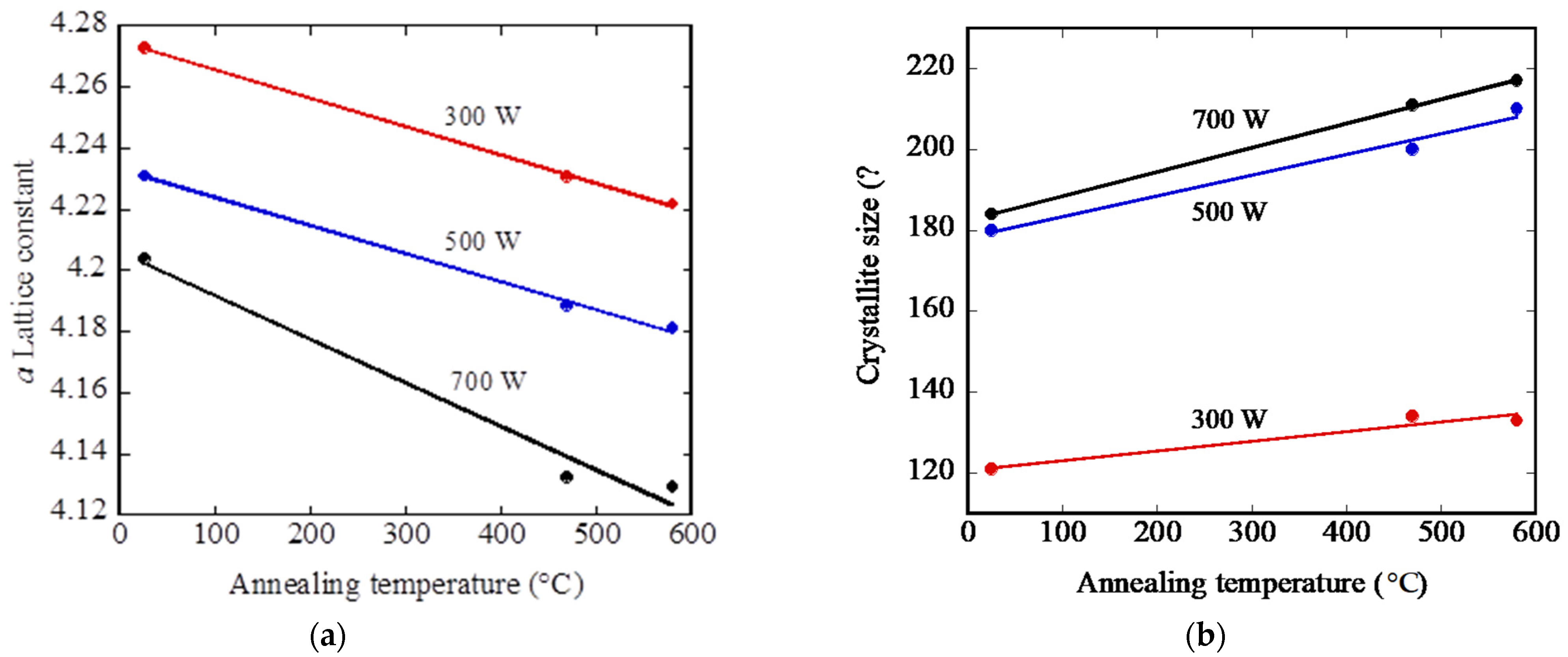
Related lattice parameters (see
Figure 4) were higher than the corresponding bulk value of the W
2N phase (4.126 Ǻ). The increase in the lattice constant can be attributed to the incorporation of excess nitrogen atoms that can occupy the vacant octahedral sites, resulting in the W
2N lattice’s expansion [
16]. The film deposited at lower deposition power consisted of small grains, whereas at higher deposition powers larger grains were present. Annealing of the deposited films resulted in an improved crystallinity of the W
2N grains and in a crystallization of the amorphous phase. The larger annealing effects on the crystallization could already observed at 470 °C; raising the temperature to 580 °C produced only a slight improvement in crystallinity.
At deposition powers of 300 and 500 W, only β-W2N was present after annealing, whereas for the material obtained at 700 W, a two-phase structure of W2N and bbc α-W appeared and the diffracted intensities increased at the higher annealing temperature. The modification seems to be progressive.
For the films obtained at a low deposition power (300 W), the preferential (111) orientation of the W
2N phase persisted after annealing, whereas when the deposition power was increased, the annealing produced not only large grains with a (111) preferential orientation, but also a further growth of grains with a (200) orientation. At a deposition power of 700 W, this effect was more pronounced. Interchanges from the preferred (111) direction to (200) have also been reported for thin niobium nitride films subjected to annealing [
17]. Nitrogen readily chemisorbs on the (200) planes but not on the N-terminated (111) planes, which reduces the flux of cations in the (200) compared to the (111) planes, resulting in the orientation of growth in the (200) direction.
Moreover, a shift of the diffraction lines towards a higher 2θ was observed after the annealing treatment for all the examined films. The shift in XRD diffraction lines, as well as the variation in intensity, could be due to the release of stresses.
The lattice constant decreased with increasing annealing temperature, indicating a relaxation of the structure due to the diffusion out of excess nitrogen atoms by means of a recrystallization process. After annealing at 580 °C, the a-lattice constant values changed from 4.273 Ǻ to 4.223 Ǻ, from 4.231 Ǻ to 4.181 Ǻ and from 4.204 Ǻ to 4.129 Ǻ for the films deposited at 300 W, 500 W and 700 W, respectively.
Only a slight change of crystallite size was observed when the annealing temperature was increased for each analyzed deposition power.
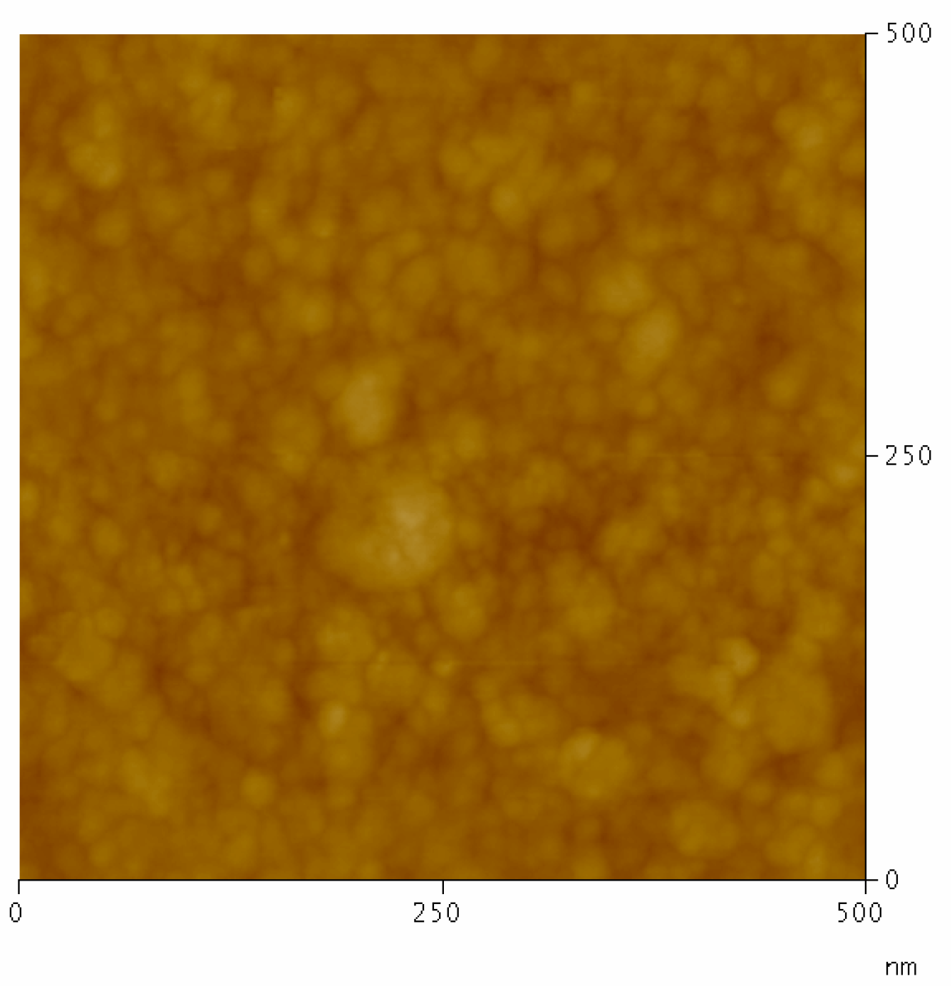
The surface morphology of the film deposited at 500 W after annealing at 580 °C is shown in
Figure 5. The surface appears smooth and consisted of rounded small grains, as expected for sputtered films, which generally tended to have a columnar microstructure.
Figure 6 shows the surface topography of the film deposited at 700 W before and after annealing treatments. After annealing at 580 °C, the amorphous film was fully crystallized and a segregation of coarse grains was evident. These grains were presumed to be α–W as it results from the X-ray diffraction shown in
Figure 3.
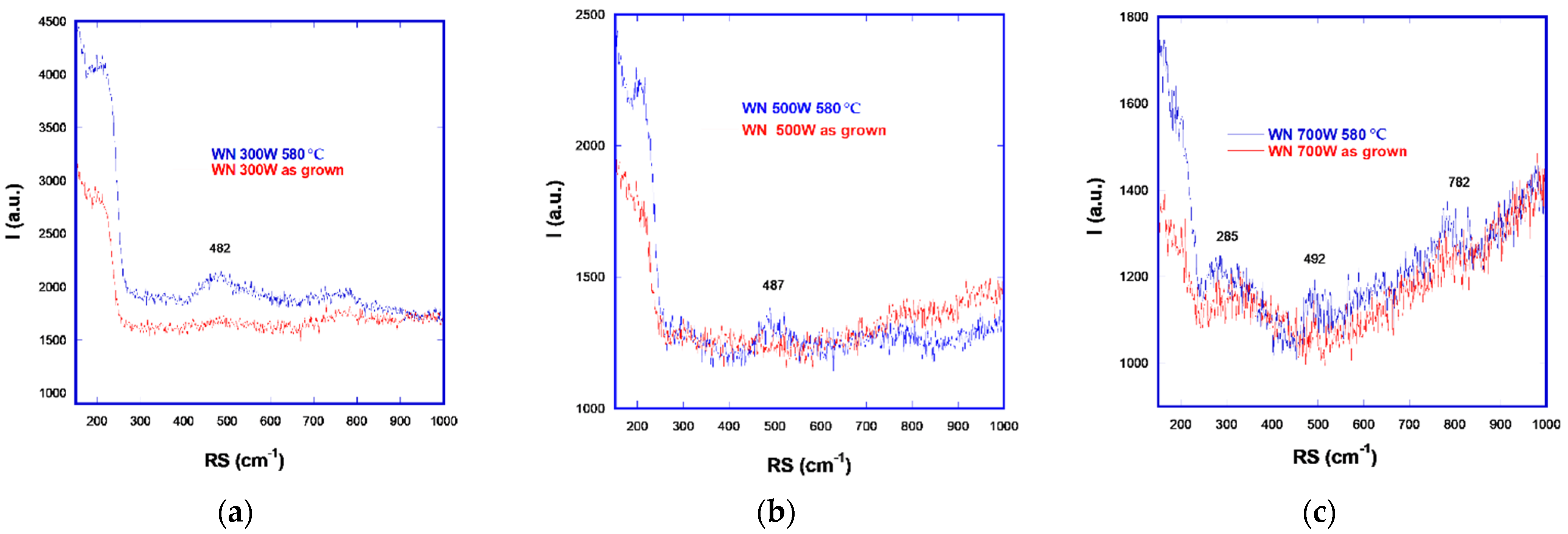
For metal nitrides that crystallize in cubic structures and ideal “perfect” crystals, first-order Raman scattering is forbidden because there is translational symmetry, q = 0, and all atoms are in centrosymmetric octahedral sites [
18]. Nevertheless, sputtered coatings are known to have vacancies that induce distortion in the structure and, as a consequence of this, the Raman spectrum is composed of broadened bands due to disorder and second-order processes. In analyzed samples there was Raman activity, so no stoichiometric cubic nitrides were present. Lattices were expanded by the effect of nitrogen adsorption. The Raman spectra of the as-grown films reported in
Figure 7 had three main regions:
With regard to the acoustic modes, their intensity is proportional to the dimensions of the crystallites. These bands should have two maxima; in Mo
2N they are reported to be 145 cm
−1 and 205 cm
−1 [
19] Acoustic bands of tungsten nitrides split after annealing into two maxima, as reported in
Table 2. In all the as-grown films, there was a unique broad band of low intensity. This behavior can be associated with an increase in crystallite size. In the 700 W film, after annealing the splitting was less accentuated with respect to the other films and a contribute at 187 cm
−1 was also present, testifying to the contribution of an amorphous phase.
The optical band located at 482 cm
−1 in the 300 W film, at 487 cm
−1 in the 500 W film and at 492 cm
−1 in the 700 W film is due to the stretching of the W-N bond. A film with a higher compressive stress shows a higher frequency shift of this band [
20]. The absence of sharp and well-defined peaks could be attributed to local disorder. With the increase in metallic character there Raman activity progressively decreases. Consistently with resistivity measurements, in the 300 W film, after annealing Raman activity increased, the film in fact became more resistive. The 500 W and 700 W films, acoustic bands aside, had an overall comparable Raman activity before and after annealing, consistent with having a similar metallic character.
As can be seen from the 700 W spectrum, after annealing there was a band at 270-280 cm
−1 RS that can be attributed to W-O bending, and a band at 780 cm
−1 that can be attributed to the W-O-W bonds stretching [
21]. The presence of such bands, indicative of an oxide phase, could be due to the presence of a tungsten phase originating from disproportion, as already discussed in relation to the XRD results. Metallic nanoparticles oxidize easily.
Figure 8 presents a comparison of FTIR reflectance before and after the two annealing steps for all films. The R% decrease is markedly more pronounced in the 500 W and 300 W samples that in the 700 W one.
FTIR reflectance in the higher-power film remained almost the same, while in both the other films it decreased after annealing. This took place because the content of W2N increases after annealing and the metallic amorphous tungsten nitride clusters crystallize, joining to the prevalent W2N phase lattice, which has a lower FTIR reflectance with respect to an amorphous phase without grain boundaries (which are able to scatter and reduce reflectance). In the high-power case, amorphous WNx crystallizes as W2N, which could diminish reflectance, but the concomitant formation of metallic tungsten, as also shown by the XRD spectra, balances this decrease by virtue of the higher FTIR reflectance of the metal, denoting an overall effect of reflectance invariance.
All the films contain simple and multiple tungsten–nitrogen bonds. For a trigonal bi-pyramidal geometry around tungsten, nitrogen ions acting as a ligands can occupy equatorial or axial sites, so the W-N bonds show short (equatorial) and long (axial) distances. The intense bands from 850 cm
−1 to 1200 cm
−1 reflect the stretching of the W-N bond, centered at 1097 cm
−1 in the 300 W and 500 W films and 1086 cm
−1 in the 700 W film. According to Wang and Andrews [
22], the signal at 1097 cm
−1 can be attributed to the W-N bond stretching in the complex (N-N)
xWN, where there is a triple bond W-N [
23]. The characteristic signature of the W
2N phase is stretching at 870 cm
−1, which was not perceived in our film joining in the aforementioned band. Of particular interest are the stretching frequencies of the bridging tungsten bonds evidenced in the inset of
Figure 9b. All the films before annealing had a characteristic strong band around 600 cm
−1 attributable to N-W-N stretching in W complexes with hosted nitrogen molecules, which is less pronounced after annealing, testifying to the evolution toward different N-W-N geometries and types of bond.
Bands located at 647 cm
−1 and 693 cm
−1, attributed to the bridging nitrogen W-N-W [
24], remained almost unchanged after annealing. In the 300 W and 500 W films at 1585 cm
−1, there was an N-H bending band. Moreover, at 1390 cm
−1, in all the films a scissoring vibration of N-H appeared. The three N-H stretching vibration bands, located at 3089 cm
−1, 3128 cm
−1 and 3253 cm
−1 in the 300 W, 500 W and 700 W films, respectively, did not change meaningfully after annealing. It is important to note that W hydrazinium complexes, of the kind W---N-NH
x, can play a role in the reduction pathway of N
2 to form nitrides.
FTIR analysis allows a general consideration of the tungsten nitridation process that takes place in plasma inside a sputtering chamber. Nitrogen reduction to form nitrides (breaking the strong N≡N and forming the azide ion [N=N=N]
−), from the chemical point of view, requires extreme conditions. The strong affinity between nitrogen and tungsten provides the driving force to form tungsten nitrides, as a result of a redox reaction between metal and molecular nitrogen. Nitrogen molecules are chemisorbed on tungsten and the triple bond is then progressively weakened. Further reduction of nitrogen proceeds with the formation of an “azo-complex”, where each nitrogen atom is bonded to metal atoms and the double bond is hence reduced to a nitride derivative. The whole process requires high temperatures or, as in the biochemical system of nitrogen fixation (where nitrogen is reduced to ammonia derivatives), the aid of an enzyme nitrogenase that uses molybdenum or tungsten cofactors [
25]. In a sputtering reactor, high vacuum conditions and ejection of reactive species from the target make nitride synthesis possible at relatively low temperatures. It is reasonable that processes at different powers should determine the formation of different-sized metallic clusters able to adsorb nitrogen and react with it. In fact the arrangement of metal atoms in a metallic cluster can exert a powerful influence on the surface chemical behavior with respect to the adsorption and dissociation of nitrogen. In other words, only a small amount of nitridation occurs by direct reaction with nitrogen-activated ions, while the greater part proceeds by a first stage of gas adsorption from different-sized metallic W clusters, followed by progressive reduction reactions. Hydrogen present in the sputtering chamber, or derived from water molecules, binds itself to the metal clusters and contributes to a minor extent to nitrogen reduction. Another aspect to be considered is that the amorphous W
xN, a solid solution of nitrogen in alpha tungsten, can itself be a target, especially at low target powers, and become sputtered itself. Once it has appeared on substrates, this amorphous phase can in turn adsorb other nitrogen and if the temperature is raised it can crystallize in W
2N, as already described for the 300 W and 500 W films, or can evolve, expelling excess nitrogen and producing metallic tungsten, like in the 700 W.
Annealing of the 700 W film at 470 °C resulted in a partial crystallization of the amorphous phase, forming a two-phase structure containing the thermodynamic one, W2N. Further annealing at 580 °C introduced a second modification: together with the W2N it a second crystalline phase, bcc W, appeared. These modifications progressed with time and temperature because they are based on redox reactions at the interfaces.
Another aspect of the evolution of tungsten nitrides after annealing can be observed when they are part of cermet materials (e.g., with AlN as the ceramic part in absorbing layers of the patented solar double nitride coatings described above [
4]). For fabricating a AlN–WN cermet, AlN material (cermet matrix) was produced at a constant cathode power, while WN
x phases dispersed in the matrix were produced by varying the cathode power (with a power value decreasing in a stepwise manner for each layer. When created in this way, a graded cermet has a high metallic content at the start and a low metallic content at the end of process. As for single materials, the same applies as for cermet and the nitridation stage of metallic W influences its stability: barely nitridated materials (700 W) after annealing can dismutate into W and W
2N, while an excess of nitrogen (300 W) undergoes crystalline readjustment with nitrogen release. For the purpose of verifying their stability inside the cermet, thin films of cermet nitrides deposited at the same three representative powers (700 W, 500 W and 300 W) were characterized by means of vibrational analysis before and after annealing. First of all, FTIR reflectance (
Figure 10) was found to depend on metallic content; in fact, cermet 700 W had the higher FTIR reflectance and cermet 300 W the lower FTIR reflectance.
After annealing, there was a decrease in FTIR reflectance for the 500 W and 700 W films, while the 300 W cermet was revealed to be stable (
Figure 11). This indicates that matrix protects metallic W
2N particles. Moreover, the NH stretching band at 3225 cm
−1 disappeared in relation to the proceeding of nitridation process. It is possible that for 700 W cermet film, inside the ceramic AlN matrix, W produced by dismutation was newly exposed to “activated” nitrogen and then newly nitridated.
Wetting experiments were performed to examine the role of electrostatic interactions on annealed WN
x-based thin films. In particular, by using the contact angle made by a droplet of two liquids, polar and nonpolar (water and di-iodomethane), on the solid surface of the samples’ basal plane, surface tension was measured, separating the London dispersion (D) and electrostatic components (P). In
Figure 12, the water contact angles (WCA°) of the three annealed WN
x samples are reported.
In
Table 3, the WCA° of various WN
x samples and AlN-based cermets are given, including those after annealing.
Surface energies, along with dispersive and electrostatic contributes, are reported in
Table 4. Moreover, a further comparison was useful for analyzing wetting behavior: the cermet 500 W before (C500-pre) and after (C500-post) annealing (for estimating the effect of thermal treatment). From the overall set of measurements, it can be outlined that:
- -
All annealed tungsten nitrides display a similar mild hydrophobic behavior, with a WCA° of around 70°, surface energies around 35 mN/m and a prevalent dispersive force but non-negligible polar contribution to wettability.
- -
AlN-based cermets containing tungsten nitride nanoparticles are much more hydrophobic with respect to single WN films in terms of the matrix behavior (AlN WCA° > 100°) with surficial energies due to prevalently dispersive forces.
A full and detailed analysis can be devoted in a future study to elucidate the frictional properties of tungsten nitrides’ basal plane for samples selected as potential electro-catalysts, as an alternative to platinum in HER water-splitting reactions.


