
Measuring the Positions of the Solder Pins of Electrical Connectors from the Side


Abstract
:Featured Application
Abstract
1. Introduction
2. Materials and Methods
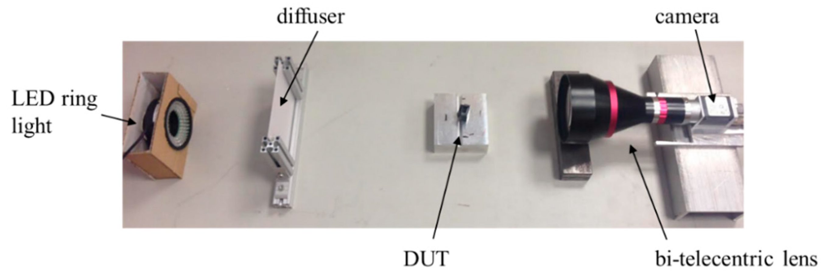
2.1. Machine Vision Systems
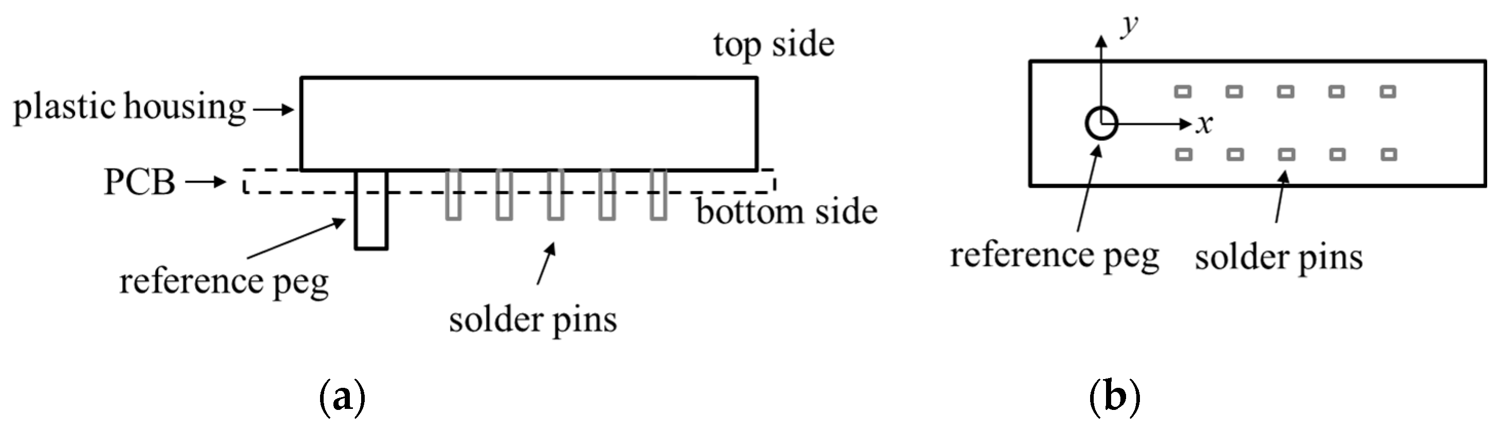
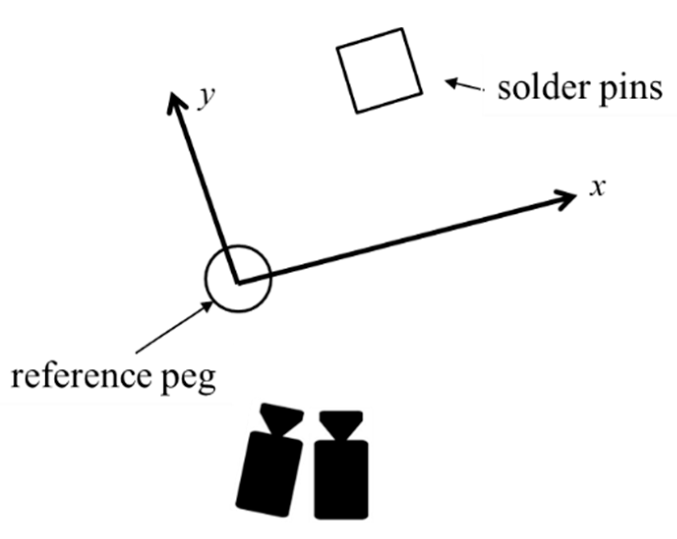
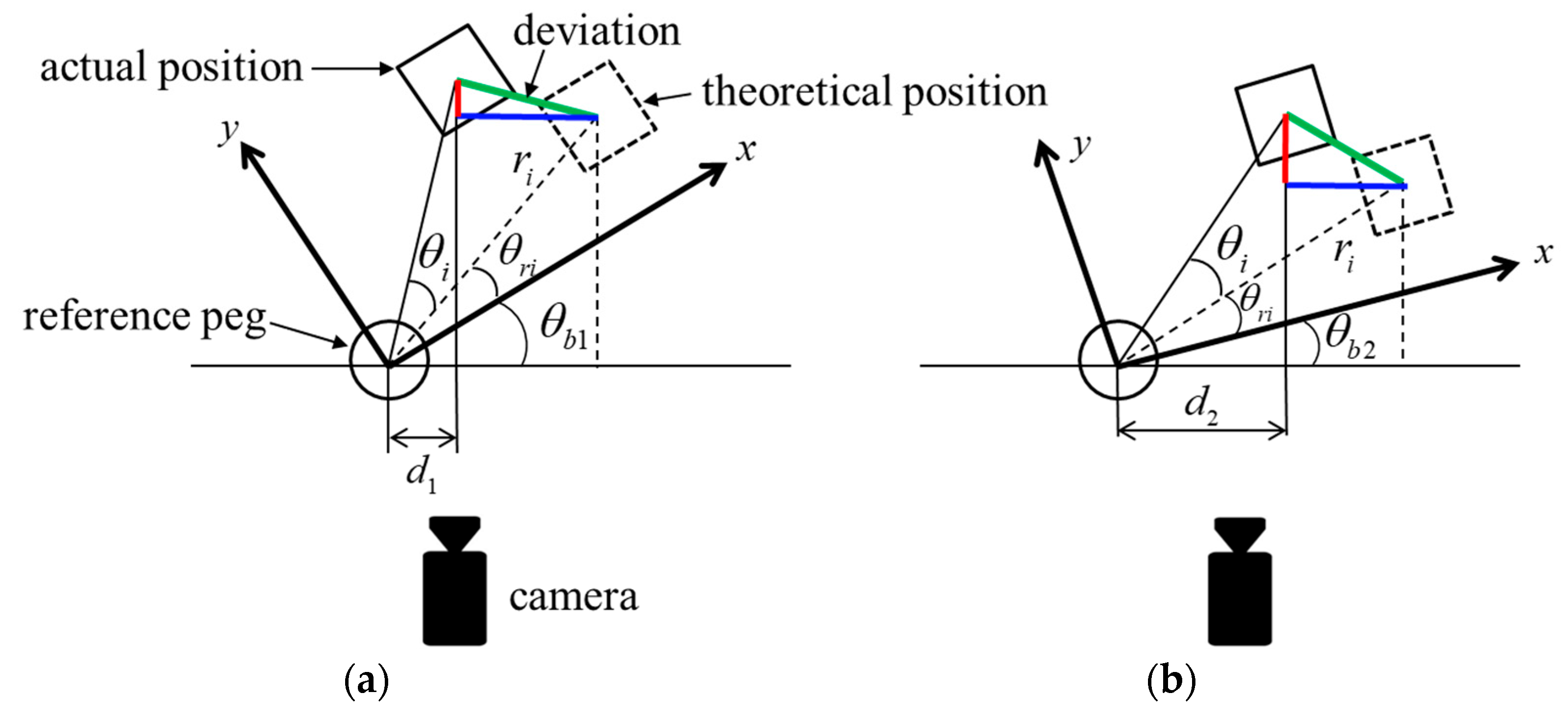
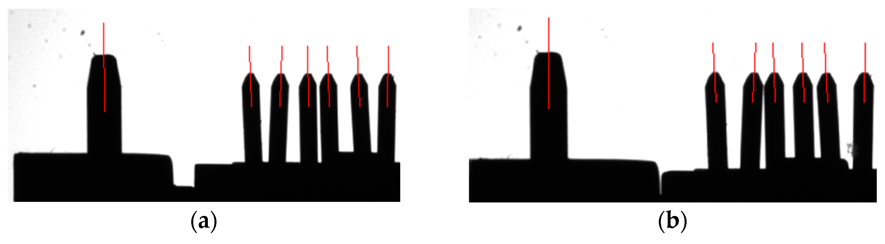
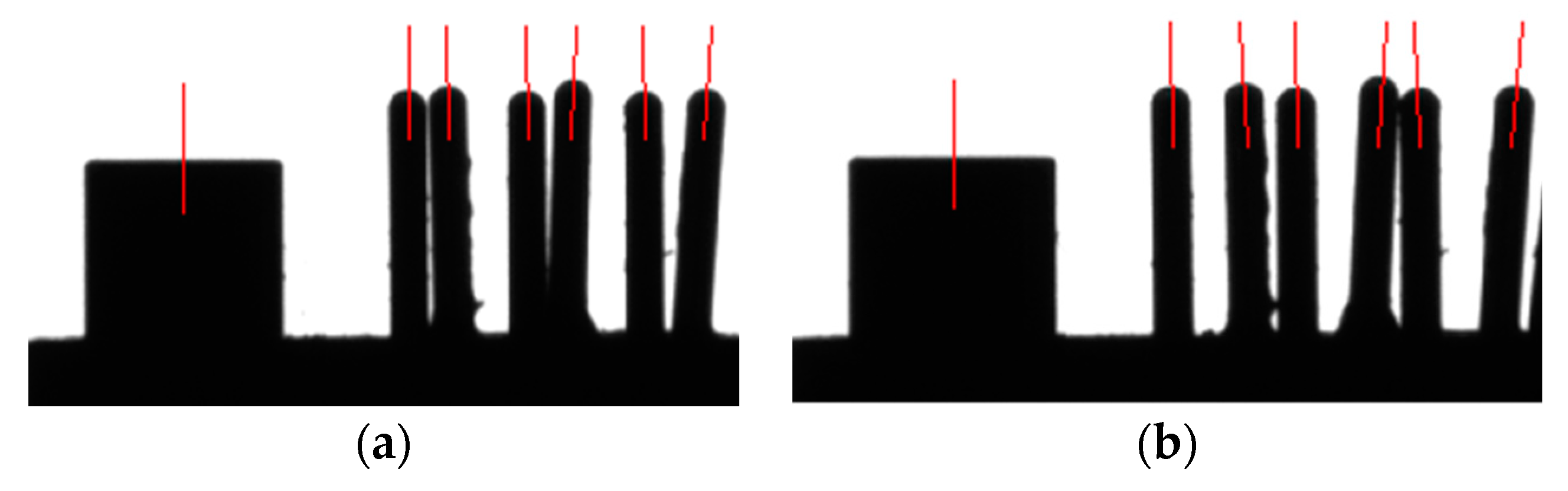
2.2. Measurement of Pins’ Positions from the Side
3. Results and Discussion
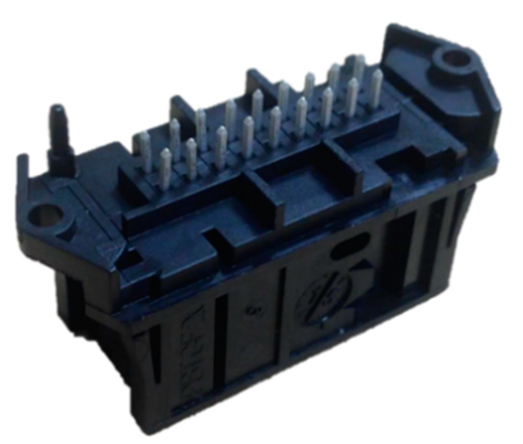
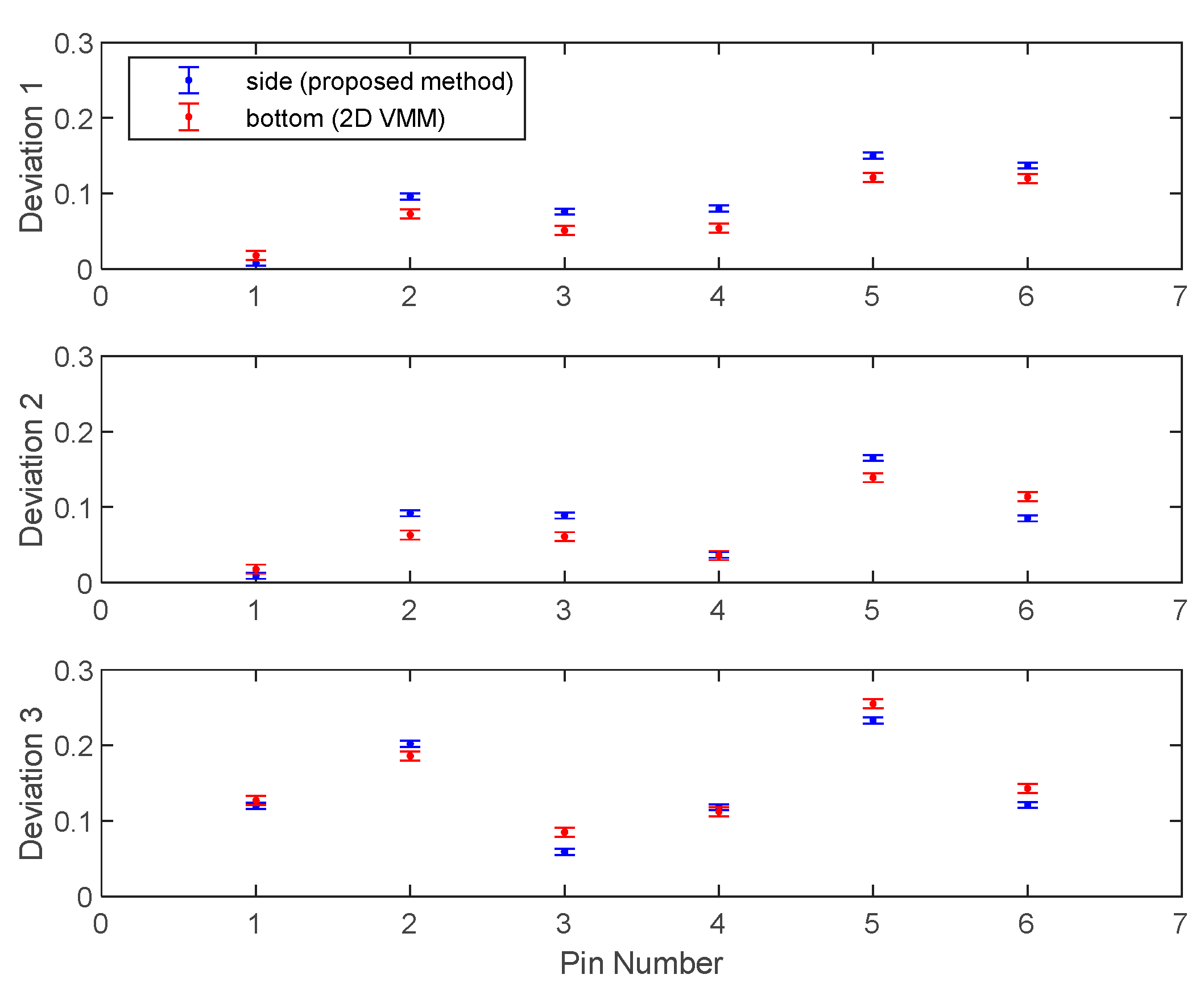
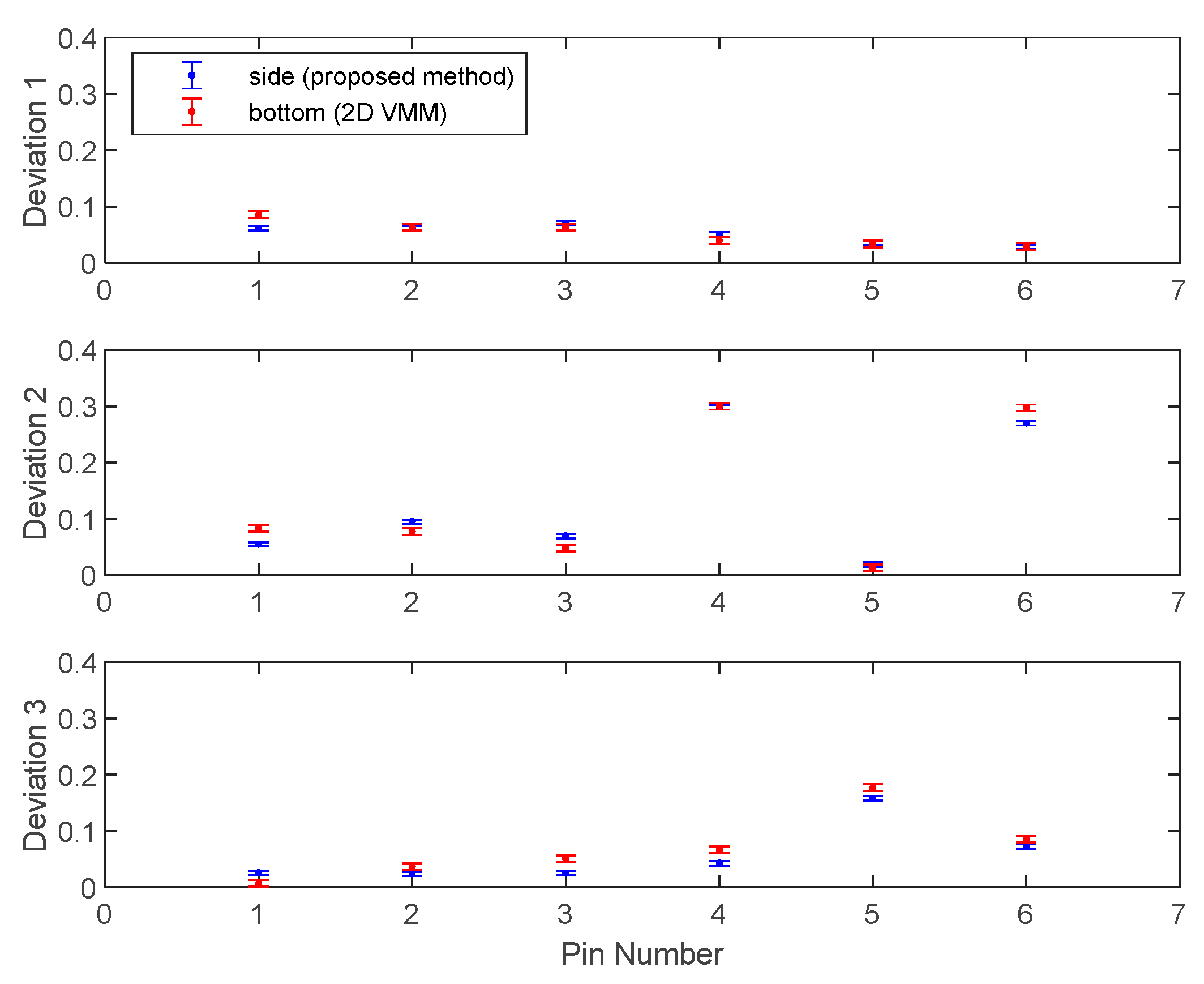
3.1. Case Study One
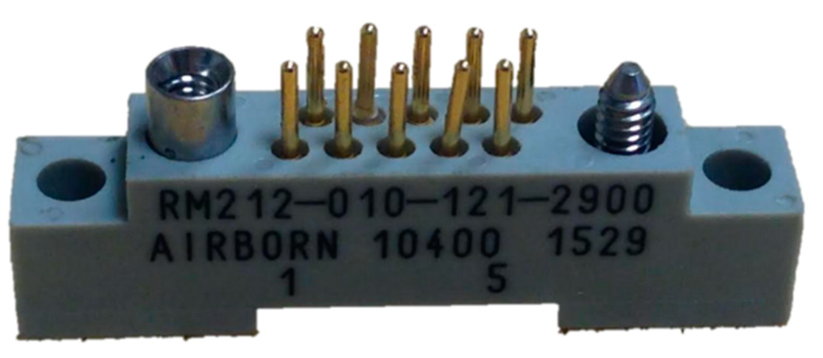
3.2. Case Study Two
3.3. Sources of Difference
4. Conclusions
Author Contributions
Funding
Institutional Review Board Statement
Informed Consent Statement
Data Availability Statement
Conflicts of Interest
References
- Zhao, D.; Feng, W.; Sun, G.; Peng, Y. High precision measurement system of micro-electronic connector based on machine vision. J. Appl. Sci. 2013, 13, 5363–5369. [Google Scholar] [CrossRef]
- Ebayyeh, A.A.R.M.A.; Mousavi, A. A Review and Analysis of Automatic Optical Inspection and Quality Monitoring Methods in Electronics Industry. IEEE Access 2020, 8, 183192–183271. [Google Scholar] [CrossRef]
- Shirmohammadi, S.; Ferrero, A. Camera as the instrument: The rising trend of vision based measurement. IEEE Instrum. Meas. Mag. 2014, 17, 41–47. [Google Scholar] [CrossRef]
- Liao, H.; Lim, Z.; Hu, Y.; Tseng, H. Guidelines of automated optical inspection (AOI) system development. In Proceedings of the 2018 IEEE 3rd International Conference on Signal and Image Processing (ICSIP), Shenzhen, China, 13–15 July 2018; pp. 362–366. [Google Scholar]
- Furukawa, Y.; Sakuma, H. Automatic detection of defects among small pins group—Inspection of connector-plug pins by the use of image processing associated with neural network. CIRP Ann. 1992, 41, 589–592. [Google Scholar] [CrossRef]
- Luo, G.; Fang, H.; Fang, Z.; Mu, G. Method for the deviation inspection of integrated circuit chip pin based on harr wavelet transform. Opt. Eng. 2000, 39, 1712–1716. [Google Scholar] [CrossRef]
- Kaitwanidvilai, S.; Saenthon, A.; Kunakorn, A. Pattern recognition technique for integrated circuit (IC) pins inspection using wavelet transform with chain-code-discrete Fourier transform and signal correlation. Int. J. Phys. Sci. 2012, 7, 1326–1332. [Google Scholar] [CrossRef]
- Huang, Y.; Pan, Q.; Liu, Q.; He, X.; Liu, Y.; Yu, Y. Application of improved Canny algorithm on the IC chip pin inspection. Adv. Mater. Res. 2011, 317–319, 854–858. [Google Scholar] [CrossRef]
- Qiao, H.; Yang, Y.; Fang, Z.L.; Liu, F.L. High-accuracy measurement of IC chip pin positions deviation based on subpixel techniques. J. Optoelectron. Laser 2002, 13, 949–952. [Google Scholar]
- Zhong, Q.; Zhang, X.; Chen, Z. Online coplanarity measurement of IC leads based on single camera vision system. Trans. Inst. Meas. Control 2016, 38, 1365–1380. [Google Scholar] [CrossRef]
- Zhong, Q.; Chen, Z.; Zhang, X.; Hu, G. Feature-based object location of IC pins by using fast run length encoding blob analysis. IEEE Trans. Compon. Packag. Manuf. Technol. 2014, 4, 1887–1898. [Google Scholar] [CrossRef]
- Ruan, Y.; Li, X.; Zhu, J. Measurement of connector terminal spacing based on machine vision. In Proceedings of the 2019 6th International Conference on Information Science and Control Engineering (ICISCE), Shanghai, China, 20–22 December 2019; pp. 371–374. [Google Scholar]
- Tay, C.J.; Kang, X.; Quan, C.; He, X.Y.; Shang, H.M. Height measurement of microchip connecting pins by use of stereovision. Appl. Opt. 2003, 42, 3827–3831. [Google Scholar] [CrossRef] [PubMed]
- Stroppa, L.; Cristalli, C. Stereo vision system for accurate 3d measurements of connector pins’ positions in production lines. Exp. Tech. 2017, 41, 69–78. [Google Scholar] [CrossRef]
- Zhao, D.; Kong, F.; Du, F. Vision-based adaptive stereo measurement of pins on multi-type electrical connectors. Meas. Sci. Technol. 2019, 30, 105002. [Google Scholar] [CrossRef]
- Beising, M. 5 important points when inspecting pins: Challenges for the 3D pin inspection with laser triangulation sensors. Opt. Photonik 2018, 13, 48–51. [Google Scholar] [CrossRef]
- Traxler, L.; Ginner, L.; Breuss, S.; Blaschitz, B. Experimental comparison of optical inline 3D measurement and inspection systems. IEEE Access 2021, 9, 53952–53963. [Google Scholar] [CrossRef]
- Li, S.; Zheng, P.; Zheng, L. An AR-assisted deep learning-based approach for automatic inspection of aviation connectors. IEEE Trans. Ind. Inform. 2021, 17, 1721–1731. [Google Scholar] [CrossRef]
- Nguyen, H.G.; Meiners, M.; Schmidt, L.; Franke, J. Deep learning-based automated optical inspection system for crimp connections. In Proceedings of the 2020 10th International Electric Drives Production Conference (EDPC), Ludwigsburg, Germany, 8–9 December 2020; pp. 1–5. [Google Scholar]
- Wu, W.; Li, Q. Machine vision inspection of electrical connectors based on improved Yolo v3. IEEE Access 2020, 8, 166184–166196. [Google Scholar] [CrossRef]
- LabVIEW. Available online: https://www.ni.com/en-us/shop/labview.html (accessed on 6 August 2022).
- BASLER. Available online: https://www.baslerweb.com/en/products/cameras/area-scan-cameras/ace/aca2500-14gm/ (accessed on 6 August 2022).
- ES Technology. Available online: http://www.esstartek.com/yellowpage/product_cg146472.html#487712 (accessed on 6 August 2022).
- Resson Technologies. Available online: https://www.resson.com.tw/en/products/detail/43 (accessed on 6 August 2022).
- TE Connectivity. Available online: https://www.te.com/usa-en/product-967618-2.html (accessed on 6 August 2022).
- AirBorn. Available online: https://www.airborn.com/board-mount/rectangular-plastic-vertical-board-mount-plug/product/294?partnumber=RM212-010-121-2900 (accessed on 6 August 2022).

| Deviation | Pin 1 | Pin 2 | Pin 3 | Pin 4 | Pin 5 | Pin 6 | |
|---|---|---|---|---|---|---|---|
| Sample 1 | side | 0.008 | 0.096 | 0.076 | 0.080 | 0.150 | 0.137 |
| bottom | 0.018 | 0.073 | 0.051 | 0.054 | 0.121 | 0.120 | |
| Sample 2 | side | 0.009 | 0.092 | 0.089 | 0.037 | 0.165 | 0.085 |
| bottom | 0.018 | 0.063 | 0.061 | 0.036 | 0.139 | 0.114 | |
| Sample 3 | side | 0.120 | 0.202 | 0.059 | 0.118 | 0.233 | 0.121 |
| bottom | 0.127 | 0.186 | 0.085 | 0.112 | 0.255 | 0.143 | |
| Deviation | Pin 1 | Pin 2 | Pin 3 | Pin 4 | Pin 5 | Pin 6 | |
|---|---|---|---|---|---|---|---|
| Sample 1 | side | 0.062 | 0.062 | 0.071 | 0.051 | 0.036 | 0.029 |
| bottom | 0.086 | 0.064 | 0.064 | 0.040 | 0.034 | 0.030 | |
| Sample 2 | side | 0.055 | 0.095 | 0.070 | 0.298 | 0.019 | 0.270 |
| bottom | 0.084 | 0.078 | 0.048 | 0.300 | 0.013 | 0.297 | |
| Sample 3 | side | 0.026 | 0.024 | 0.025 | 0.043 | 0.158 | 0.073 |
| bottom | 0.007 | 0.037 | 0.051 | 0.067 | 0.177 | 0.086 | |
Publisher’s Note: MDPI stays neutral with regard to jurisdictional claims in published maps and institutional affiliations. |
© 2022 by the authors. Licensee MDPI, Basel, Switzerland. This article is an open access article distributed under the terms and conditions of the Creative Commons Attribution (CC BY) license (https://creativecommons.org/licenses/by/4.0/).
Share and Cite
Lee, W.-c.; Huang, K.-C. Measuring the Positions of the Solder Pins of Electrical Connectors from the Side. Appl. Sci. 2022, 12, 8772. https://doi.org/10.3390/app12178772
Lee W-c, Huang K-C. Measuring the Positions of the Solder Pins of Electrical Connectors from the Side. Applied Sciences. 2022; 12(17):8772. https://doi.org/10.3390/app12178772
Chicago/Turabian StyleLee, Wei-chen, and Kuan-Chuan Huang. 2022. "Measuring the Positions of the Solder Pins of Electrical Connectors from the Side" Applied Sciences 12, no. 17: 8772. https://doi.org/10.3390/app12178772
APA StyleLee, W.-c., & Huang, K.-C. (2022). Measuring the Positions of the Solder Pins of Electrical Connectors from the Side. Applied Sciences, 12(17), 8772. https://doi.org/10.3390/app12178772