Article

Low-Frequency Terahertz Photonic Crystal Waveguide with a Lilac-Shaped Defect Based on Stereolithography 3D Printing

1
Tianjin Key Laboratory of Optoelectronic Detection Technology and System, School of Electronic and Information Engineering, Tiangong University, Tianjin 300387, China
2
Institute of Fluid Physics, China Academy of Engineering Physics, Mianyang 621900, China
3
Department of Laboratory Medicine, Southwest Hospital, Third Military Medical University (Army Medical University), Chongqing 400038, China
4
Key Laboratory of Opto-Electronics Information Technology (Ministry of Education), School of Precision Instruments and Opto-Electronic Engineering, Tianjin University, Tianjin 300072, China
*
Authors to whom correspondence should be addressed.
Appl. Sci. 2022, 12(16), 8333; https://doi.org/10.3390/app12168333
Submission received: 26 July 2022 / Revised: 14 August 2022 / Accepted: 16 August 2022 / Published: 20 August 2022
(This article belongs to the Special Issue Optoelectronic Materials, Devices, and Applications)

Abstract

:
Terahertz (THz) photonic crystal (PC) waveguides show promise as an efficient and versatile waveguiding platform for communication, sensing, and imaging. However, low-frequency THz PC waveguides with a low-cost and easy fabrication remain challenging. To address this issue, a THz PC waveguide with a lilac-shaped defect has been designed and fabricated by 3D printing based on stereolithography (SLA). The reflection and transmission characteristics of the proposed waveguide have been analyzed using the finite difference frequency domain (FDFD) method. The waveguide spectral response is further optimized by changing the distance of the lilac-shaped resonant cavities. Consistent with the results of numerical modeling, the measured results show that the waveguide performs a resonant reflection in the region of 0.2 to 0.3 THz and low-pass transmission in the 6G mobile communication window. Furthermore, in order to characterize the performance of the proposed waveguide, parameters have been analyzed, including the Q factor, resonant frequency, and bandwidth. This work supplies a novel pathway for the design and fabrication of a low-frequency THz PC waveguide with potential applications in communication, sensing, and imaging.

1. Introduction

Terahertz (THz) is electromagnetic radiation with a frequency in the range 0.1 to 10 THz, which lies in the gap between the microwave and infrared regions [1]. THz technology has been playing an increasingly important role in various fields, including wireless communication, security, biomedical applications, imaging, sensing, and spectroscopy [2,3,4]. Although THz waves have proven to be beneficial for many applications, most THz systems are based on free-space optics that are complex, delicate, and require frequent alignment [1]. To solve these issues, different types of THz waveguides have been proposed. Many of THz waveguides have been demonstrated for applications such as communication, sensing, and imaging. Notably, the THz band from 0.1 to 0.3 THz has been of significant research interest in recent years, as it is considered to be the main transmission band for 6G telecommunication; low-frequency THz waveguides working in the 6G mobile communication window are gaining immense demand [5]. Currently, the very limited design library of conventional waveguide structures substantially constraints their functionalities to mostly mere waveguiding. Researchers are still struggling to design and manufacture high-performance waveguides with a low-cost and easy fabrication [3].
A variety of waveguides have been explored, including metallic and dielectric waveguides [4,6,7,8,9,10,11,12]. Most metallic waveguides are only suitable for millimeter lengths [13], because of the strong trade-off between mode confinement and metallic loss [11,12]. Because of the existing surface plasmon polaritons (SPPs) [12], metallic PCs enable confinement of THz waves in the sub-millimeter scale. However, metallic PC waveguides are still inevitably accompanied by Ohmic losses, which limit the quality factors of resonance and compromise the efficiency of metallic-based devices [8]. In the past few years, a growing number of reports have shown that this problem could be solved by employing dielectric waveguides, which mostly rely on high-index and low-loss particles (such as silicon, SiO2, and TiO2) [7,9,10]. Consequently, interest in dielectric waveguides has increased with the application of dielectric antennas, resonators, polarizers, etc. [4,8,9,10,14]. Meanwhile, a number of researches have been focused on dielectric waveguides because of the wide variety of available materials and the greater flexibility of the waveguide design. Many dielectric waveguide structures, including planar [15], rectangular [16], circular [1], strip [17], and photonic crystal waveguides [10,18,19] have been investigated. Among them, photonic crystals can realize strong light confinement due to the nature of photonic band gaps, and show great potential in high-performance dielectric waveguides [10].
Currently, THz waveguides are mostly fabricated by photolithography, which requires multiple steps, including spin-coating, prebaking, the preparation of masks, exposure, etc. [20,21,22], leading to a long preparation cycle and a high cost [16,23]. In addition, most of these devices have a substrate, which significantly lowers the transmittance and causes internal interference. Therefore, it is of great significance that THz PC waveguides are fabricated in a simple, low-cost, and efficient way [16]. Furthermore, most of the related works are conducted at a microwave and millimeter wave; it remains challenging to obtain low-frequency THz PC waveguides with a low-cost and easy fabrication. Direct writing technology has been applied to create complex THz waveguides, such as microfluidic three-dimensional photonic crystals [24]. High-accuracy 3D printing based on stereolithography (SLA) [13,23,25,26,27] as an emerging technology shows great potential in high-performance dielectric waveguides, but it has not been applied in THz PC waveguides.
In this work, a THz PC waveguide with a lilac-shaped defect is demonstrated. This proposed waveguide is fabricated with a high-density photosensitive resin by 3D printing based on SLA. The reflection and transmission properties of the waveguide in the 6G mobile communication window have been investigated. The waveguide spectral response is optimized by changing the distance of the lilac-shaped resonant cavities. The waveguide performance in the range of 0.1 THz to 0.5 THz has been analyzed, including the Q factors, resonant frequency (fR), full width half max (FWHM), −60 dB bandwidth, and loss.

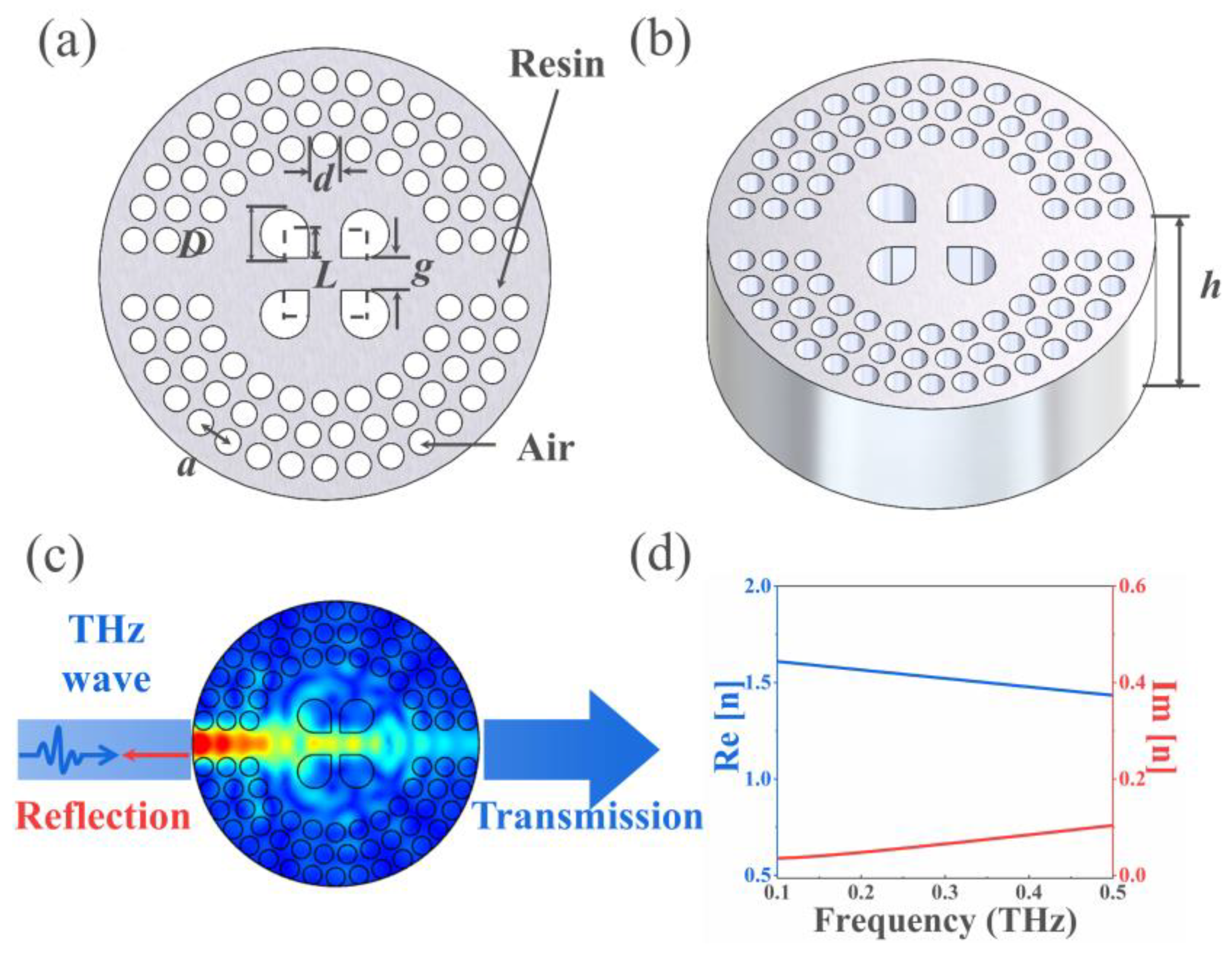
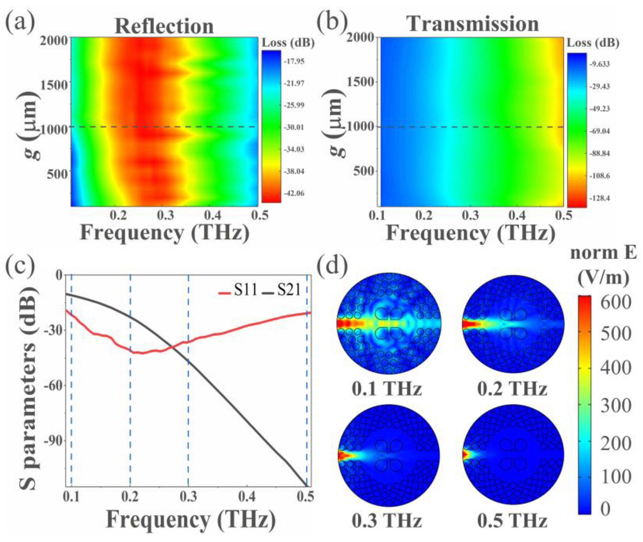
2. Design and Simulations

In this part, a low-frequency THz PC waveguide with a lilac-shaped defect is designed, as shown in Figure 1a,b. The symmetrical petal hollow core is induced in the waveguide structure to broaden the operation frequency bandwidth. For efficiently guiding the terahertz wave, the structural parameters are optimized to design a suitable structure. The lattice structure of the periodically arranged unit cells consists of air holes on the o-xy plane, which are described by the following [28,29]
x M , m = a M cos 2 m π 6 M
y M , m = a M sin 2 m π 6 M
where a is the lattice constant, M is the number of the air hole rings, and m (1 ≤ m ≤ 6M) is the number of the air holes in the Mth ring. The lilac-shaped resonant cavities are formed by four larger symmetrical air holes at the center, with the first, second, and third rings of the periodically arranged unit holes removed. Each resonant cavity consists of an intersection of one circular air hole with a diameter of D and one square air hole with a length of L. The gap distance between four petals of the lilac-shaped resonant cavities is defined as g. Initial values of the structure parameters are a = 1000 µm, d = 0.8 a = 800 µm, D = 1500 µm, L = 750 µm, and g = 500 µm. Meanwhile, the depth of the air holes in the z direction is much larger than a (h >> a).
In the simulation process, the optical characteristics of the THz PC waveguide were analyzed using COMSOL Multiphysics. The boundary condition was set to the scattering boundary condition to absorb energies. The physics-controlled mesh was applied to the model [29]. The process of the reflection and transmission characteristics of the proposed waveguide is shown in Figure 1c. The TE-polarized Gaussian form was injected into the waveguide from the left side and a monitor was set on the right side of the waveguide. Air holes were placed throughout the photosensitive resin background. In the simulation, the refractive index (RI) of the photosensitive resin used in the range of 0.1 to 0.5 THz were measured using the Terahertz Time-Domain Spectroscopy (THz-TDS) system (Menlo TeraSmart, Martinsried, Germany), which is shown in Figure 1d.
The gap distance (g) is an important parameter that can change the photonic bandgap of the photonic crystal; in particular, the guidance of the terahertz wave in the waveguide is caused by the photonic bandgap mechanism. Therefore, in order to explore the detailed functionality of the waveguide, the influence of the gap distance (g) has been simulated from 100 µm to 2000 µm in steps of 100 µm. The reflection map of the waveguide with different gap distances is shown in Figure 2a. As the gap distance increases from 100 µm to 2000 µm, the reflection loss performs a resonant dip in the frequency region of 0.2 to 0.3 THz. Correspondingly, as shown in Figure 2b, the transmission loss increases continually within 0.5 THz. For instance, when the gap distance is 1000 µm, the reflection loss (S11) and transmission coefficient (S21) are shown in Figure 2c. The band-stop behavior of the proposed waveguide is analyzed by the reflection loss. The resonant frequency of the band-stop is approximately at 0.23 THz with a transmission loss of about −44 dB. The transmission coefficient shows the low-pass behavior. To better understand the reflection and transmission effect, the simulated electric field patterns at different frequencies are analyzed in Figure 2d when g is 1000 µm. It is observed that the THz wave can smoothly pass through this waveguide within 0.2 THz and it is reflected mostly higher than 0.3 THz.

3. Experiment and Results

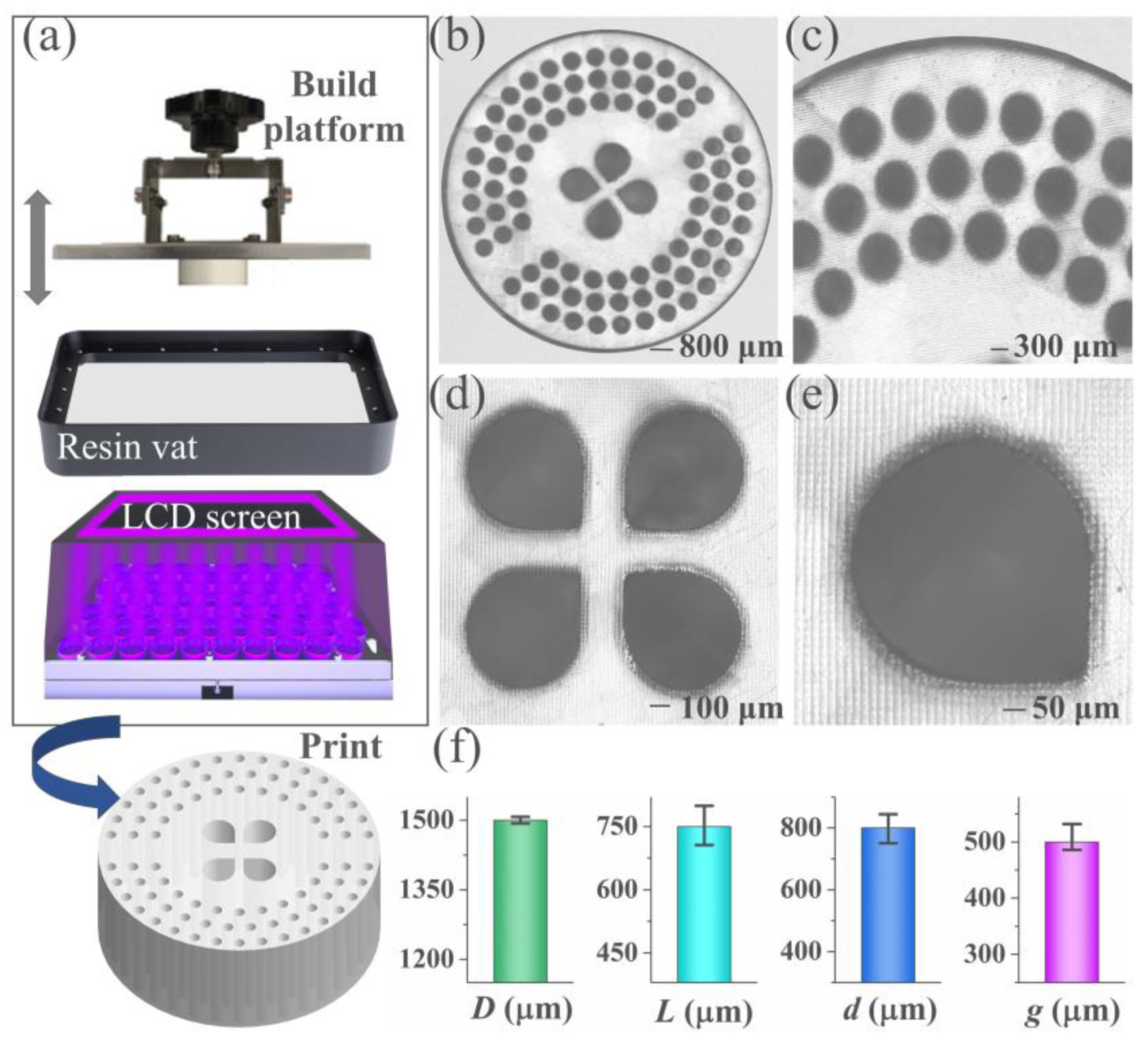
3.1. Fabrication of the Proposed Waveguides

The exact reproduction of the designed structure requires tremendous efforts to optimize the parameters of the facility. Fortunately, 3D printing is a process of making prototype parts directly from computer models, which opens up almost unlimited possibilities for rapid prototyping [13]. In this study, waveguides with the gap distance (g) set as 500 µm, 1000 µm, and 2000 µm, respectively, were printed using the SLA 3D printing mechanism. Figure 3a shows an overview of the entire 3D printing methodology [25,26]. Figure 3b–e shows a cross-section of the optical electron microscopy (OEM) images of the waveguide (e.g., the gap distance g is 500 µm). The fabricated error of the waveguide structure was measured using a microscope camera to evaluate the accuracy of the dimensions [27]. The OEM results proved that the morphology of the 3D-printing was consistent with the design. According to the measurement result, as shown in Figure 3f, d = 800 ± 14.96 µm, D = 1500 ± 19 µm, L = 750 ± 18.74 µm, g = 500 ± 14.23 µm. It is noted that the difference between the measured and designed dimensions was within the allowable printer error (<50 µm). Therefore, the fabrication method of the proposed waveguide had the advantages of a low-cost and easy fabrication, and flexible design. These properties are desirable for applications of various terahertz devices [30].

3.2. 3D Printing Based on Stereolithography
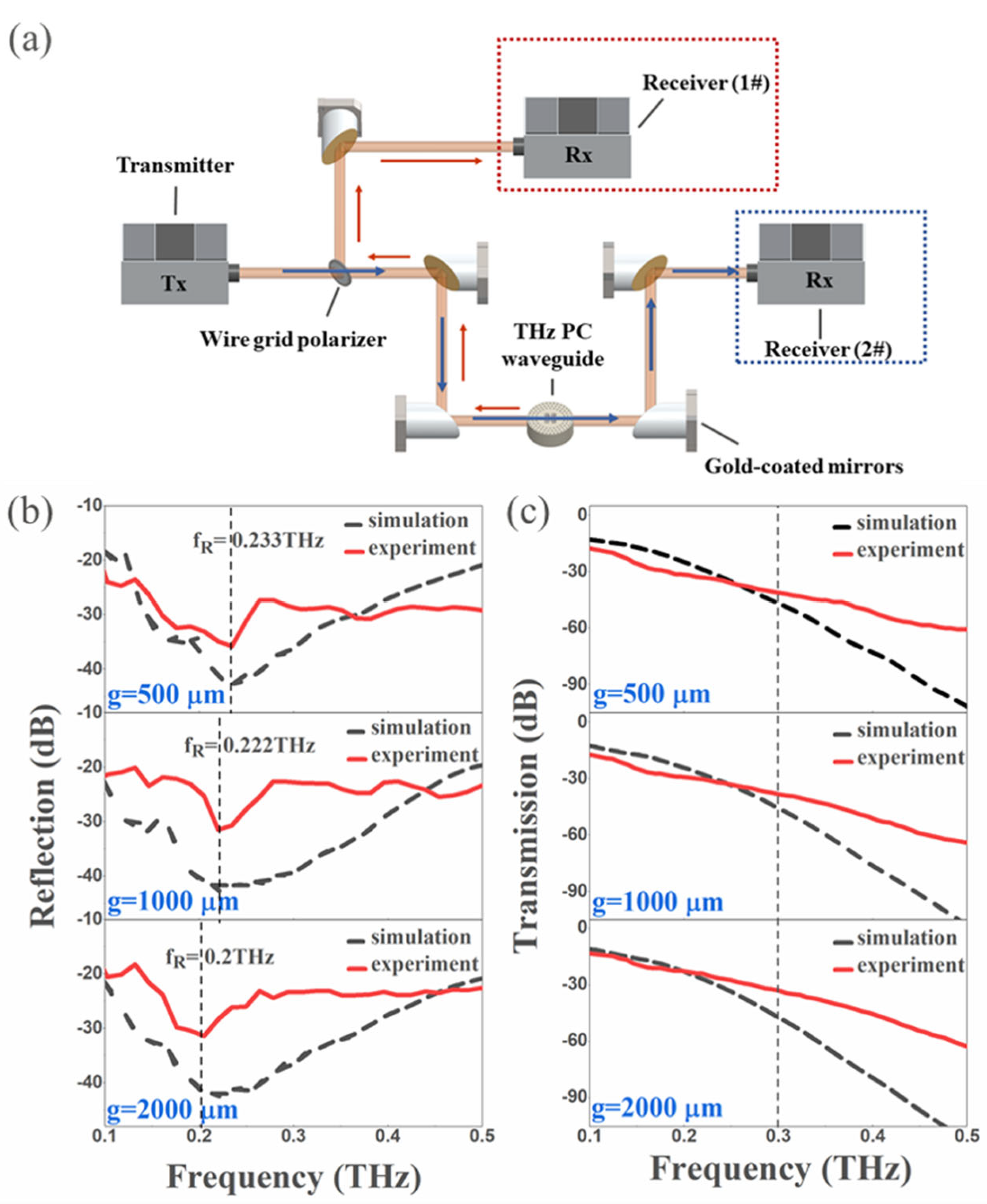
The desired waveguide devices were first drafted using commercial CAD drawing software and then translated into STL format, a suitable file for a 3D printer. The file was then sliced in a Z direction using the Photon Workshop software (Version 2.1.23.RC8). The sliced file was then sent to the 3D printer. This SLA printer (ANYCUBIC Photon Mono X) used an inverted lithography set-up with a 405 nm UV light irradiation and LCD screen selective voxel curing that resulted in the finished 3D structure [26]. The transverse resolution was 47 µm and the longitudinal resolution was 1.25 µm (i.e., along the structure height) [23].

3.3. THZ-TDS Setup

All of the experimental investigations were performed with a THz-TDS system (Menlo TeraSmart, Martinsried, Germany). The centered wavelength of the femtosecond laser that was used was 780 nm and the repetition rate was 100 MHz. The frequency resolution of the THz-TDS system was 1.2 GHz with a signal to noise ratio (SNR) of about 80 dB. The beam was guided between the transmitter and detector by off-axis parabolic mirrors.

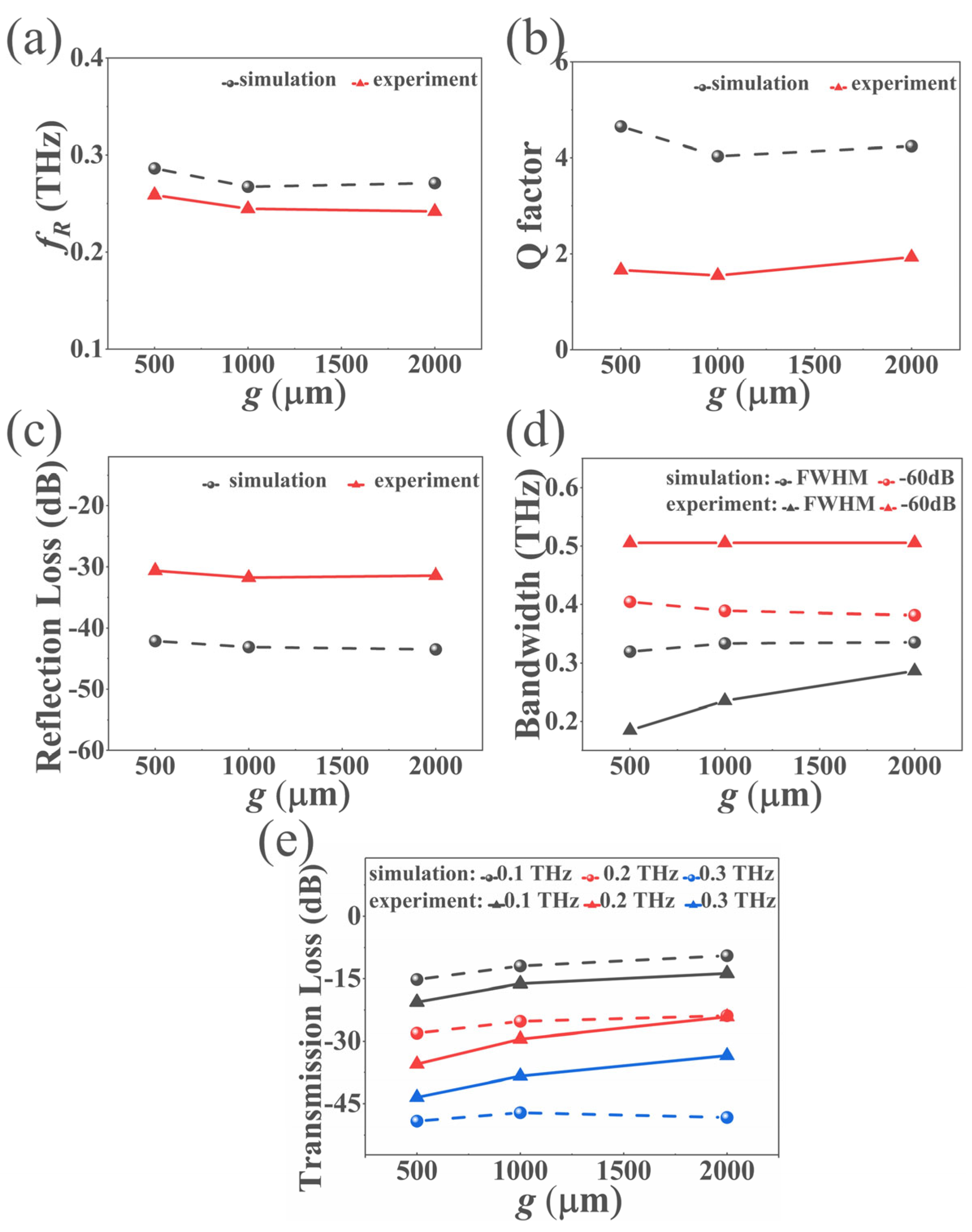
3.4. Measurement and Discussion

As shown in Figure 4a, in the measurement of reflection loss, the signal is measured by receiver (1#), which is set at the reflection optical path (red arrows). For measurement of the transmission loss, the signal is measured by the receiver (2#) that is set at the transmission optical path (blue arrows). The RI of the photosensitive resin material used in THz frequency range were measured by the THz-TDS system. As shown in Figure 4b,c, the experimental and simulated loss of the proposed waveguide with different gap distances were obtained from 0.1 to 0.5 THz in the potential 6G telecommunication band.
In the reflection spectra, it was found that the resonant frequency (fR) of the waveguide shifted to the left with an increase in gap distance (g), which is shown in Figure 4b. The experimental and simulated resonant frequency were both in the region of 0.2 to 0.3 THz. The numerical simulation results showed that the reflection loss decreased by about −20 dB, and the experimental results showed that it decreased by about −10 dB. As shown in Figure 4c, in the transmission spectra from 0.1 to 0.3 THz, it was found that the experimental and simulated results demonstrated approximately the same loss, of less than −45 dB, and it showed a remarkable decrease trend higher than 0.3 THz. The magnitudes of loss observed in the experimental results did not exactly match that of the simulated results, and this discrepancy could be attributed to the detection limitation of the experimental apparatus. Overall, the numerical simulation results agreed well with the experimental results, which indicates that the proposed waveguide has a good controllable performance.
To analyze the resonant performance of the waveguide, the Q factor and reflection loss at the resonant frequency were calculated. Q factor can be expressed by [30]
Q = ω r FWHM
where ωr is the resonant frequency (ωr = 2πfR) and FWHM is the full width half max of the resonant spectrum. As shown in Figure 5a, the resonant frequency has a shift of 33 GHz. Simultaneously, as shown in Figure 5b, with a gap distance of 500–2000 µm, the measured Q factor was obtained from 1.55 to 2. The reflection loss was further analyzed at the resonant frequency, as shown in Figure 5c. The difference in the reflection loss between the experimental and simulated results was about 10 dB.
In order to better understand the transmission characteristics of the waveguide, the FWHM and the −60 dB bandwidth were analyzed. As shown in Figure 5d, with a gap distance of 500–1000 µm, FWHM was obtained from 0.2 to 0.3 THz. The −60 dB bandwidth was obtained from 0.4 to 0.5 THz, which is within the detection limitation of most commercial THz-TDS systems. In addition, in order to better illustrate the performance of the transmission loss in diverse frequency conditions, the transmission loss was analyzed in detail at different frequencies within 0.3 THz, individually (Figure 5e). The results revealed that the transmission loss decreased with a larger gap distance, and a similar trend was also indicated by the simulation results. The above results show that the waveguide performance could be controlled by the gap distance. Thus, the optimum structural parameters of the waveguide should be selected according to the application requirements.

4. Conclusions

In conclusion, a THz PC waveguide with a lilac-shaped defect is demonstrated in this work. The reflection and transmission characteristics of the proposed waveguide have been analyzed both in simulation and experiment. The waveguide spectral response is further optimized by changing the distance of the lilac-shaped resonant cavities. The designed waveguide performs a resonant reflection in the region of 0.2 to 0.3 THz and a low-pass transmission in the 6G mobile communication window. These results have demonstrated that the waveguide performance can be controlled by the gap distance. For some special occasions, the gap distance can be treated in order to evaluate the pros and cons of this device. In addition, the proposed waveguide has many advantages, including a designable structure, low-cost and easy fabrication, and operation in a low-THz frequency. Although its reflection and transmission loss are larger than other types of waveguides, the performance of the proposed waveguide will be optimized with the development of SLA technology. It holds great promise for extensive applications in communication, sensing, and imaging.

Author Contributions

Conceptualization, J.S. and Y.D.; methodology, J.S., Y.D. and X.L. (Xiuyan Li); software, H.B., X.L. (Xianguo Li), and W.F. (Wei Fan); validation, L.T., W.F. (Weiling Fu), and X.Y.; writing—original draft preparation, J.S. and Y.D.; writing—review and editing, J.S., X.Y. and P.N.; visualization, W.F. (Weiling Fu); supervision, P.N. and J.Y. All authors have read and agreed to the published version of the manuscript.

Funding

This work is sponsored by the National Natural Science Foundation of China (61905177, 61901297, 61903273, and 81802118); the Natural Science Foundation of Tianjin City (19JCQNJC01400); the Open Research Fund of National Mobile Communications Research Laboratory, Southeast University (2022D12); and the Open Fund of IPOC, BUPT (IPOC2021B02).

Institutional Review Board Statement

Not applicable.

Informed Consent Statement

Not applicable.

Data Availability Statement

Not applicable.

Conflicts of Interest

The authors declare no conflict of interest.

References

  1. Talataisong, W.; Gorecki, J.; van Putten, L.D.; Ismaeel, R.; Williamson, J.; Addinall, K.; Schwendemann, D.; Beresna, M.; Apostolopoulos, V.; Brambilla, G. Hollow-core antiresonant terahertz fiber-based TOPAS extruded from a 3D printer using a metal 3D printed nozzle. Photonics Res. 2021, 9, 1513. [Google Scholar] [CrossRef]
  2. Yudasari, N.; Anthony, J.; Leonhardt, R. Terahertz pulse propagation in 3D-printed waveguide with metal wires component. Opt. Express 2014, 22, 26042–26054. [Google Scholar] [CrossRef] [PubMed]
  3. Lu, Y.; Feng, X.; Wang, Q.; Zhang, X.; Fang, M.; Sha, W.E.I.; Huang, Z.; Xu, Q.; Niu, L.; Chen, X.; et al. Integrated Terahertz Generator-Manipulators Using Epsilon-near-Zero-Hybrid Nonlinear Metasurfaces. Nano Lett. 2021, 21, 7699–7707. [Google Scholar] [CrossRef] [PubMed]
  4. Li, J.; Zheng, C.; Li, J.; Wang, G.; Liu, J.; Yue, Z.; Hao, X.; Yang, Y.; Li, F.; Tang, T.; et al. Terahertz wavefront shaping with multi-channel polarization conversion based on all-dielectric metasurface. Photonics Res. 2021, 9, 1939. [Google Scholar] [CrossRef]
  5. Lee, Y.S.; Choi, H.; Kim, B.; Kang, C.; Maeng, I.; Oh, S.J.; Kim, S.; Oh, K. Low-Loss Polytetrafluoroethylene Hexagonal Porous Fiber for Terahertz Pulse Transmission in the 6G Mobile Communication Window. IEEE Trans. Microw. Theory Tech. 2021, 69, 4623–4630. [Google Scholar] [CrossRef]
  6. Gu, T.; Andryieuski, A.; Hao, Y.; Li, Y.; Hone, J.; Wong, C.W.; Lavrinenko, A.; Low, T.; Heinz, T.F. Photonic and Plasmonic Guided Modes in Graphene–Silicon Photonic Crystals. ACS Photonics 2015, 2, 1552–1558. [Google Scholar] [CrossRef]
  7. Han, S.; Cong, L.; Srivastava, Y.K.; Qiang, B.; Rybin, M.V.; Kumar, A.; Jain, R.; Lim, W.X.; Achanta, V.G.; Prabhu, S.S.; et al. All-Dielectric Active Terahertz Photonics Driven by Bound States in the Continuum. Adv. Mater. 2019, 31, e1901921. [Google Scholar] [CrossRef]
  8. Lan, C.; Ma, H.; Wang, M.; Gao, Z.; Liu, K.; Bi, K.; Zhou, J.; Xin, X. Highly Efficient Active All-Dielectric Metasurfaces Based on Hybrid Structures Integrated with Phase-Change Materials: From Terahertz to Optical Ranges. ACS Appl. Mater. Interfaces 2019, 11, 14229–14238. [Google Scholar] [CrossRef]
  9. Withayachumnankul, W.; Fujita, M.; Nagatsuma, T. Integrated Silicon Photonic Crystals Toward Terahertz Communications. Adv. Opt. Mater. 2018, 6, 1800401. [Google Scholar] [CrossRef] [Green Version]
  10. Yokoo, A.; Takiguchi, M.; Birowosuto, M.D.; Tateno, K.; Zhang, G.; Kuramochi, E.; Shinya, A.; Taniyama, H.; Notomi, M. Subwavelength Nanowire Lasers on a Silicon Photonic Crystal Operating at Telecom Wavelengths. ACS Photonics 2017, 4, 355–362. [Google Scholar] [CrossRef]
  11. Reinhard, B.; Torosyan, G.; Beigang, R. Band structure of terahertz metallic photonic crystals with high metal filling factor. Appl. Phys. Lett. 2008, 92, 201107. [Google Scholar] [CrossRef]
  12. Su, X.; Xu, Q.; Lu, Y.; Zhang, Z.; Xu, Y.; Zhang, X.; Li, Y.; Ouyang, C.; Deng, F.; Liu, Y.; et al. Gradient Index Devices for Terahertz Spoof Surface Plasmon Polaritons. ACS Photonics 2020, 7, 3305–3312. [Google Scholar] [CrossRef]
  13. Yang, J.; Zhao, J.; Gong, C.; Tian, H.; Sun, L.; Chen, P.; Lin, L.; Liu, W. 3D printed low-loss THz waveguide based on Kagome photonic crystal structure. Opt. Express 2016, 24, 22454–22460. [Google Scholar] [CrossRef] [PubMed]
  14. Cheben, P.; Halir, R.; Schmid, J.H.; Atwater, H.A.; Smith, D.R. Subwavelength integrated photonics. Nature 2018, 560, 565–572. [Google Scholar] [CrossRef] [PubMed]
  15. Lin, Y.; Yao, H.; Ju, X.; Chen, Y.; Zhong, S.; Wang, X. Free-standing double-layer terahertz band-pass filters fabricated by femtosecond laser micro-machining. Opt. Express 2017, 25, 25125–25134. [Google Scholar] [CrossRef] [PubMed]
  16. Headland, D.; Yu, X.; Fujita, M.; Nagatsuma, T. Near-field out-of-plane coupling between terahertz photonic crystal waveguides. Optica 2019, 6, 1002–1011. [Google Scholar] [CrossRef]
  17. Yee, C.; Jukam, N.; Sherwin, M. Transmission of single mode ultrathin terahertz photonic crystal slabs. Appl. Phys. Lett. 2007, 91, 194104. [Google Scholar] [CrossRef]
  18. Fan, K.; Xu, X.; Gu, Y.; Dai, Z.; Cheng, X.; Zhou, J.; Jiang, Y.; Fan, T.; Xu, J. Organic DAST Single Crystal Meta-Cavity Resonances at Terahertz Frequencies. ACS Photonics 2019, 6, 1674–1680. [Google Scholar] [CrossRef]
  19. Gangnaik, A.S.; Georgiev, Y.M.; Holmes, J.D. New Generation Electron Beam Resists: A Review. Chem. Mater. 2017, 29, 1898–1917. [Google Scholar] [CrossRef]
  20. Huang, Y.; Zhao, Q.; Kalyoncu, S.K.; Torun, R.; Lu, Y.; Capolino, F.; Boyraz, O. Phase-gradient gap-plasmon metasurface based blazed grating for real time dispersive imaging. Appl. Phys. Lett. 2014, 104, 161106. [Google Scholar] [CrossRef] [Green Version]
  21. Paniagua-Dominguez, R.; Yu, Y.F.; Khaidarov, E.; Choi, S.; Leong, V.; Bakker, R.M.; Liang, X.; Fu, Y.H.; Valuckas, V.; Krivitsky, L.A.; et al. A Metalens with a Near-Unity Numerical Aperture. Nano Lett. 2018, 18, 2124–2132. [Google Scholar] [CrossRef] [PubMed] [Green Version]
  22. Liu, D.; Zhao, S.; You, B.; Jhuo, S.S.; Lu, J.Y.; Chou, S.; Hattori, T. Tuning transmission properties of 3D printed metal rod arrays by breaking the structural symmetry. Opt. Express 2021, 29, 538–551. [Google Scholar] [CrossRef] [PubMed]
  23. Ju, X.; Yang, W.; Gao, S.; Li, Q. Direct Writing of Microfluidic Three-Dimensional Photonic Crystal Structures for Terahertz Technology Applications. ACS Appl. Mater. Interfaces 2019, 11, 41611–41616. [Google Scholar] [CrossRef] [PubMed]
  24. Liu, X.; Tao, J.; Liu, J.; Xu, X.; Zhang, J.; Huang, Y.; Chen, Y.; Zhang, J.; Deng, D.Y.B.; Gou, M.; et al. 3D Printing Enabled Customization of Functional Microgels. ACS Appl. Mater. Interfaces 2019, 11, 12209–12215. [Google Scholar] [CrossRef] [PubMed]
  25. Ruiz, A.J.; Garg, S.; Streeter, S.S.; Giallorenzi, M.K.; LaRochelle, E.P.M.; Samkoe, K.S.; Pogue, B.W. 3D printing fluorescent material with tunable optical properties. Sci. Rep. 2021, 11, 17135. [Google Scholar] [CrossRef]
  26. Wang, R.; Yang, W.; Gao, S.; Ju, X.; Zhu, P.; Li, B.; Li, Q. Direct-writing of vanadium dioxide/polydimethylsiloxane three-dimensional photonic crystals with thermally tunable terahertz properties. J. Mater. Chem. C 2019, 7, 8185–8191. [Google Scholar] [CrossRef]
  27. Yan, D.; Meng, M.; Li, J.; Wang, Y. Proposal for a symmetrical petal core terahertz waveguide for terahertz wave guidance. J. Phys. D Appl. Phys. 2020, 53, 275101. [Google Scholar] [CrossRef]
  28. Yan, D.; Meng, M.; Li, J.; Wang, Y. Terahertz wave refractive index sensor based on a sunflower-type photonic crystal. Laser Phys. 2020, 30, 066206. [Google Scholar] [CrossRef]
  29. Ye, L.; Zhang, W.; Ofori-Okai, B.K.; Li, W.; Zhuo, J.; Cai, G.; Liu, Q.H. Super Subwavelength Guiding and Rejecting of Terahertz Spoof SPPs Enabled by Planar Plasmonic Waveguides and Notch Filters Based on Spiral-Shaped Units. J. Lightwave Technol. 2018, 36, 4988–4994. [Google Scholar] [CrossRef]
  30. Sultana, J.; Islam, M.S.; Cordeiro, C.M.B.; Habib, M.S.; Dinovitser, A.; Kaushik, M.; Ng, B.W.H.; Ebendorff-Heidepriem, H.; Abbott, D. Hollow Core Inhibited Coupled Antiresonant Terahertz Fiber: A Numerical and Experimental Study. IEEE Trans. Terahertz Sci. Technol. 2021, 11, 245–260. [Google Scholar] [CrossRef]
Figure 1. (a) The 2D structure of the THz PC waveguide. (b) The 3D structure of the THz PC waveguide. (c) The process of reflection and transmission characteristics of the THz PC waveguide. (d) The real and imaginary parts of the refractive index (RI) of the photosensitive resin.
Applsci 12 08333 g001
Figure 2. (a,b) The 2D contour maps of simulated reflection loss and transmission loss as a function of frequency with different gap distances (g), respectively. The black dashed line indicates g = 1000 µm. (c) The simulated S parameters of the THz PC waveguide with g = 1000 µm. These blue dashed lines indicate the frequency at 0.1 THz, 0.2 THz, 0.3 THz, and 0.5 THz, respectively. (d) Electric field distributions of the THz PC waveguide at g = 1000 µm with different frequencies (0.1 THz, 0.2 THz, 0.3 THz, 0.5 THz, respectively).
Applsci 12 08333 g002
Figure 3. (a) Schematic of the SLA printing process and 3D printed object. Optical microscopy images of (b) the cross-section of the THz PC waveguide, (c) the periodically arranged unit cells of the THz PC waveguide, (d) the lilac-shaped resonant cavities of the THz PC waveguide, and (e) one petal of the lilac-shaped resonant cavities of the THz PC waveguide. (f) Statistical analysis of the size of four parameters after multiple measurements.
Applsci 12 08333 g003
Figure 4. (a) Optical path for the THz-TDS measurement setup, the above experiments are performed in dry air. (b) The simulated and experimental reflection spectra for the THz PC waveguide with the gap distance (g) set as 500 µm, 1000 µm, and 2000 µm, respectively. (c) The simulated and experimental transmission spectra for the THz PC waveguide with the gap distance (g) set as 500 µm, 1000 µm, and 2000 µm, respectively.
Applsci 12 08333 g004
Figure 5. Characteristics of the THz PC waveguide. Influence of the gap distance (g) on (a) the resonant frequency fR, (b) Q factor, (c) the reflection loss (at f = fR), (d) the bandwidth (with FWHM and −60 dB bandwidth, respectively), and (e) the transmission loss with f = 0.1 THz, f = 0.2 THz, and f = 0.3 THz, respectively.
Applsci 12 08333 g005
Publisher’s Note: MDPI stays neutral with regard to jurisdictional claims in published maps and institutional affiliations.

