Article

AFM/XPS Analysis of the Growth and Architecture of Oriented Molecular Monolayer by Spin Cast Process and Its Cross-Linking Induced by Hyperthermal Hydrogen

1
Shanghai Technical Institute of Electronics & Information, Shanghai 201411, China
2
Faculty of Materials Science and Technology, Kunming University of Science and Technology, Kunming 650093, China
3
School of Materials Science and Engineering, Shanghai University, Shanghai 200444, China
4
Solmont Technology Wuxi Co., Ltd., 228 Linghu Blvd., Tian’an Tech Park, A1-602, Xinwu District, Wuxi 214135, China
5
Surface Science Western, The University of Western Ontario, London, ON N6G 0J3, Canada
6
Shunde Graduate School, University of Science and Technology Beijing, Foshan 528399, China
*
Author to whom correspondence should be addressed.
Appl. Sci. 2022, 12(12), 6233; https://doi.org/10.3390/app12126233
Submission received: 22 April 2022 / Revised: 16 June 2022 / Accepted: 16 June 2022 / Published: 19 June 2022
(This article belongs to the Special Issue Self-Assembled Monolayers (SAMs) and Their Applications)

Abstract

:
We used atomic force microscopy (AFM) and X-ray photoelectron spectroscopy (XPS) to comprehensively study the growth and the cross-linking of dotriacontane (C32H66) nanofilms that were deposited on a silicon wafer by the spin-coating process. It was found that the molecular structure of the nanofilms changed with C32H66 concentration at the given spin speed, of which a monolayer of oriented C32H66 molecules, formed at lower deposition concentrations, was composed of a perpendicular orientation state with the molecular long-chain axis perpendicular to the substrate surface and a parallel orientation state, while the perpendicular state was essentially dominant when the nanofilm was formed at higher deposition concentrations. The shortening of the first perpendicular layer in AFM topography could be attributed to the mixing of both parallel and perpendicular lamellas in the first layer. XPS analysis indicated that the average thickness of the layer almost linearly increased with the C32H66 concentration. The monolayer of C32H66 film could be cross-linked by a hyperthermal hydrogen-induced cross-linking (HHIC) at a few eV via kinetic collision to cleave C-H bonds. The water contact angle measurement of extensive HHIC on C32H66 nanofilms disclosed that the static contact angle decreased with the treatment time (or fluence) and saturated after full cross-linking of the film.

1. Introduction

N-alkane nanofilms supported on solid substrates have been extensively studied both experimentally [1,2,3,4,5,6,7,8,9,10,11,12,13] and theoretically [14,15] since the last decade. Interesting points for these studies are not only its fundamental importance for n-alkane as a main constituent of many molecules with industrial (e.g., as the principal constituents of commercial lubricants [16]) and biological relevance, as well as constituents in lots of polymers (as prototypes of more complex polymers) used in coatings, adhesives, and electronic devices, but also its interfacial structure at the molecular level, which acted as the desirable temporary masks to protect surfaces owing to the physisorbed and easily removed characteristic [17]. This is because the long-chain hydrocarbon plays an important role in the structure formation process, such as the crystallization of fats and polymers, and the formation of lipid membranes. Most of the past studies focused on the fundamental understanding of the structure formation of hydrocarbons based on a simple long-hydrocarbon-chain molecule, such as n-alkane, and all the studies related to different lengths of the n-alkane molecules and substrates concluded that long-hydrocarbon-chain molecules were arranged in an ordered lamellar structure, in which the molecular long-chain axes were parallel to each other due to the van de Waals interaction among the molecules, and their end groups were on same plane. Two typical preferred molecular orientation states were observed on substrate surfaces, to the highly attractive surface, e.g., metal and HOPG, and very thin n-alkane was found to crystallize with their molecular axes parallel to the substrate [15], while for intermediate-length n-alkane prepared on SiO2 (Si wafer with native oxides), it was found that the chains were dominantly perpendicular to the substrate, proposed by Riegler and co-workers [1,2,3,4]. Taub’s group also proposed that for intermediate-length-chain alkane molecules on SiO2, there is one or two molecular layers of the parallel chains underneath [5,6,7,8,9]. Very recently, a Monte Carlo simulation by Yamamoto et al. [15] suggested that the crystalline films consist of thin crystalline lamellae where chains are either parallel or perpendicular to the substrate. The relative number of the lamella types is dependent on film thickness, substrate attraction, and crystallization temperature. They concluded that the thicker films on substrates of higher attraction comprise dominantly parallel lamellae, while thinner films on substrates with weaker attraction prefer perpendicular lamellae. Nozaki et al. [10] demonstrated very recently that, based on vacuum-evaporation-deposited n-alkane (n = 23–27) thin film, using X-ray diffraction (XRD) and atomic force microscopy (AFM) analysis, there is only a perpendicularly orientated state at a high substrate temperature and a low evaporation rate, while the films are composed by the “co-existence” of both perpendicular and parallel states at lower temperatures. They concluded that the perpendicular state is the most thermodynamically stable state. The thin films of n-alkane can be prepared both by liquid (wet chemistry, dip coating based on physical absorption, and/or spin casting) and dry (evaporation in vacuum) methods on a Si wafer (with native oxide layer), Ag, In, and HOPG. However, spin casting used for preparing the nanofilms of n-alkane, as a very simple method, still lacks a systematic study, such as a systematic study of n-alkane films with different thicknesses prepared by spin casting. Meanwhile, the preparation and study of the monolayer of n-alkane films prepared by spin casting has barely been reported. Herein, we have designed and prepared the n-alkane films with different thicknesses from a sub-monolayer to multilayer by spin casting systematically and established a method to control the film thickness.
Previously, the n-alkane films were studied by several advanced analytical techniques, including scanning tunnelling microscopy (STM) [11], AFM [8,18], XRD [3,10,12], high-resolution ellipsometry [5], and synchrotron X-ray scattering [6,7,19] analysis. It is obvious that STM and AFM techniques provide the localized surface microstructure of the layers, while XRD, high-resolution ellipsometry, and synchrotron X-ray scattering results reflect average information of the surface microstructure. Thus, it is meaningful to combine the analyses both in localized and large-area regions for completely understanding the growth of the thin films, especially the thin films with different thickness. Meanwhile, X-ray photoelectron spectroscopy (XPS) has previously been little used to study the detailed information of well-organized n-alkane molecular layers. Herein, the organized molecular films have been characterized by both AFM and XPS, especially based on C1s peak-shape analysis and the change in the film thickness. We found that the first C32H66 thin films are comprised of the coexistence of parallel-oriented-state and perpendicular-oriented-state molecular lamellae in our preparation condition, which settled the dispute about the C32H66 heights measured by AFM [8,18].
In addition, the n-alkane films in previous research were all formed by the van der Waals force (just physical absorption). Thus, these n-alkane films are loose and their application is limited. In this work, we utilized a new green technology of hyperthermal hydrogen-induced cross-linking (HHIC) [20] to successfully make the C32H66 molecules be firmly connected, and the cross-linking process was studied by AFM and XPS in detail. The collapse and re-organization in well-organized molecular films induced by HHIC were observed, and AFM/XPS analyses suggested that HHIC made C32H66 cross-link and link more compactly without changing the film thickness, while its XPS effective thickness did not change.

2. Materials and Methods

C32H66, hexane, ethanol, and acetone with a nominal purity of 98% were purchased from Aldrich and used without purification. C32H66 was dissolved into hexane under magnetic stirring, to keep its concentration varying from 0.05% w/v to 0.5% w/v. Fresh n-type Si wafers with a length/width of 10 × 10 mm2 and a SiO2 layer about 1–2 nm in height were obtained by ultrasonic cleaning in ethanol, acetone for 30 min each, and then drying at 60 °C. A 50 μL solution was casted on a Si wafer surface, spun at 5000 rpm until it transformed into a film, and the final C32H66 nanofilm was obtained after drying at 60 °C for 4 h.
Cross-linking experiments were conducted on a home-made electron cyclotron resonance ECR-enhanced microwave plasma reactor, which uses extraction ions to fill a space fully with H2 gas to collide and exchange its kinetic energy to hydrogen. This process may produce H with some certain kinetic energy and/or H2 having more kinetic energy. The energetic hydrogen breaks C-H bonds and then all C radicals will produce cross-linking. The bombardment fluence of hyperthermal hydrogen on the samples was estimated by the extraction voltage (as primary H+ kinetic energy) and collision numbers, which depend on the distance between extraction grids, sample surface, and the pressure, for a given extraction voltage. One of the bombarded C32H66 samples was soaked, washed by hexane, and then dried with compressed N2. All samples were sent to XPS and AFM characterization ex situ. Direct evidence of the cross-linking was to be identified if there was any C32H66 film remaining in the surface after washing by hexane.
XPS was carried out with a Kratos Axis Ultra spectrometer using a monochromatic Al Kα source (8 mA, 14 kV). High-resolution spectra of the core level were recorded using a 0.05 eV step, 20 eV pass energy, and an analysis area of 300 μm × 700 μm, while survey spectra were recorded at a 0.7 eV step, 160 eV pass energy, and analysis area of 300 μm × 700 μm. AFM topographic images were obtained in an area of 5 μm × 5 μm using a Park Systems (Model: XE-100) operated in the noncontact mode. We used a noncontact cantilever with a nominal spring constant of 40 N/m and the tip was pyramidal in shape with a radius of 10 nm at the apex.
Wettability of the surfaces was evaluated through contact angle measurement using a Rame-hart 100 goniometer. Drops (10 μL) of deionized water were placed into the surfaces via a micrometer syringe (Gilmont Instrument). At least three measurements on each of the two identically treated samples were taken and averaged.

3. Results

3.1. Surface Morphology of the C32H66 Thin Films by AFM

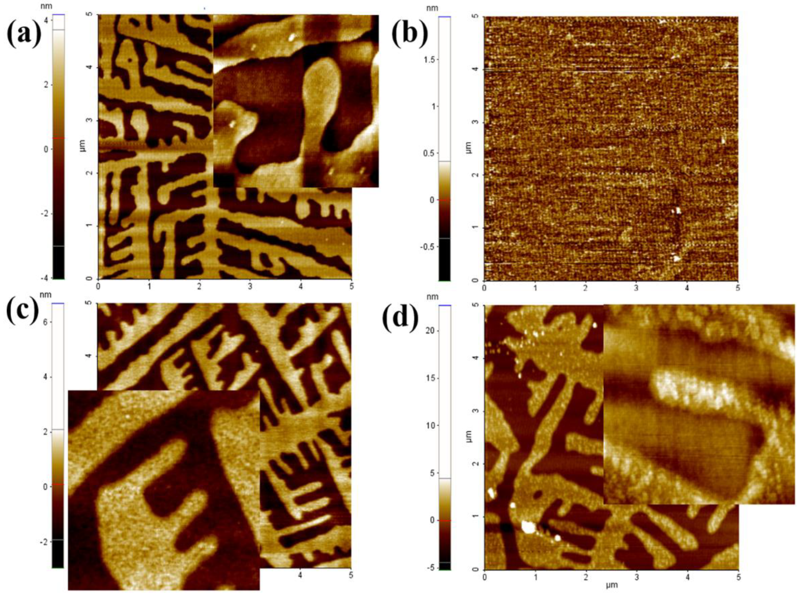
Although Taub’s group had extensively studied [8,18] the surface morphology of C32H66 by contact and noncontact AFM using two different thicknesses, 6.5 nm and 9.5 nm, by the dipping coating physical absorption process, their studies were not concentrated on monolayers or sub-monolayers and a series of films with different thicknesses. Here, we prepared a series of samples with different average thicknesses from 2.4 nm (sub-monolayer) to 10.5 nm by changing the C32H66 concentration at a given spin-coating speed. Though the thickness of the films was estimated by XPS, AFM topographic images provided useful information on the thickness and coverage of the alkane film. Typical AFM images and a couple of profiles isolated from the images are shown in Figure 1, as well as in Figures S1 and S2 (Supporting Information). They showed that the topographies were composed of dendrites (relatively low C32H66 concentration) or island-like structures, which is consistent with Taub’s AFM results [8,18] and Nozaki’s AFM data [10]. These surface features could be attributed to perpendicularly oriented C32H66 molecules. Our AFM measurement noise on the Si wafer (without coating anything) was about ±0.1 nm (see Figure S3).
Shown in Figure 1a,b are two AFM images for samples made with lower C32H66 concentrations (0.05 and 0.13 w/v, respectively). Self-assembled monolayers (SAMs) of C32H66 were observed. AFM images were flattened line by line along the fast scan direction (x-axis), allowing accurate measurements of the thickness of the monolayers from 10 profiles isolated from the image. The thickness of the monolayers estimated by using this approach for both images was 3.9 ± 0.2 nm. Also shown in these two figures are two representative profiles isolated from each of the two images. The thickness and coverage of the monolayers could also be estimated from the histogram and bearing ratio, respectively. For example, the histogram and bearing ratio of Figure 1b are shown in Figure S4. The height rises seen in Figure 1b were excluded for calculations of the histogram and bearing ratio. The histogram suggested that the thickness of the monolayers was 3.9 nm and the bearing ratio indicated that the coverage of the monolayers was approximately 68%.
Our AFM results showed that the long-chain alkane molecules self-assembled on the substrate, even though there were no interactions between the methyl groups and the hydrophilic silicon substrate. This suggested that the van der Waals forces between the long methylene chains dictated the assembly of the alkane molecules. Due to the lack of interactions between the molecules in this type of SAM and the substrate, they were susceptible to solvent, which would be discussed later.
With an increased concentration, as shown in Figure 1c (0.3% w/v), the formation of multiplayers was observed. The thickness of the top monolayers in the multilayer structure was 4.3 ± 0.1 nm, which was slightly thicker than that (3.9 ± 0.2 nm) of the monolayers over the substrate seen in Figure 1a,b. This indicated that the molecules in the monolayers on the Si substrate (Figure 1a,b) tilted more than those in the top monolayers of the multilayers (Figure 1c). It was intriguing that the first monolayer contacting the substrate in Figure 1c (the groove-like features located at lower left and upper right) had a lower thickness of 3.4 ± 0.1 nm (Figure 1c and Figure S1).
When the C32H66 concentration was increased to 0.5% w/v, as shown in Figure 1d, multilayers were seen. The topography of this sample was similar to that shown in Figure 1c, except for more stacked layers. The profiles isolated from the AFM image showed that the highest layers were more than 20 nm. Therefore, for studying C32H66 SAMs, we selected samples made with lower concentrations.
Figure 2 shows the results of the cross-linking of C32H66 SAMs induced by HHIC, which is one of physical collision-inducing C-H bond breaking and forms C-C cross-linking [21,22,23]. Insets are their AFM images under a small scanning scale (1 µm × 1 µm). The C32H66 SAMs seen in Figure 2a were completely removed from the Si substrate upon hexane rinse, shown in Figure 2b. This was a reflection that the alkane SAMs were simply physisorbed on the substrate so that the molecules were dissolved in hexane. Upon cross-linking of the alkane molecules, as shown in Figure 2c, the topography of SAMs remained largely similar to that of the pristine SAMs. Figure 2d shows that the cross-linked SAMs survived the hexane rinse. In this case, even though there were no interactions between the SAMs and the substrate, the SAMs themselves were now not soluble in hexane.
Although there was little change for the bombarded C32H66 layer (Figure 2c) in the surface morphology shown in AFM images (Figure 2), a certain increase in the surface roughness, based on a scanning line noise analysis (one could see that the height of the line profiling increased from ±0.2 nm to ±0.3 nm), had been evidenced. Surface morphologies of the treated and washed C32H66 layers (Figure 2d) showed a significant increase in surface roughness in the perpendicular layer from ±0.2 nm (as-deposited) to ±0.5 nm or even as high as to ±1 nm (Figure S5). There were a lot of aggregated nanoparticles or clusters appearing in the perpendicular region, although it was not able to find any thickness change by XPS estimation within experimental errors. We noted that the “bulk particles” (for example, nanoparticles as high as ~40 nm in Figure 1b,d) density and dimension in the film increased with C32H66 concentration and their orientation was always in a perpendicular state. Meanwhile, we also noted that the perpendicular layer was always not completed in each layer.

3.2. Surface Chemical Composition of the C32H66 Thin Films

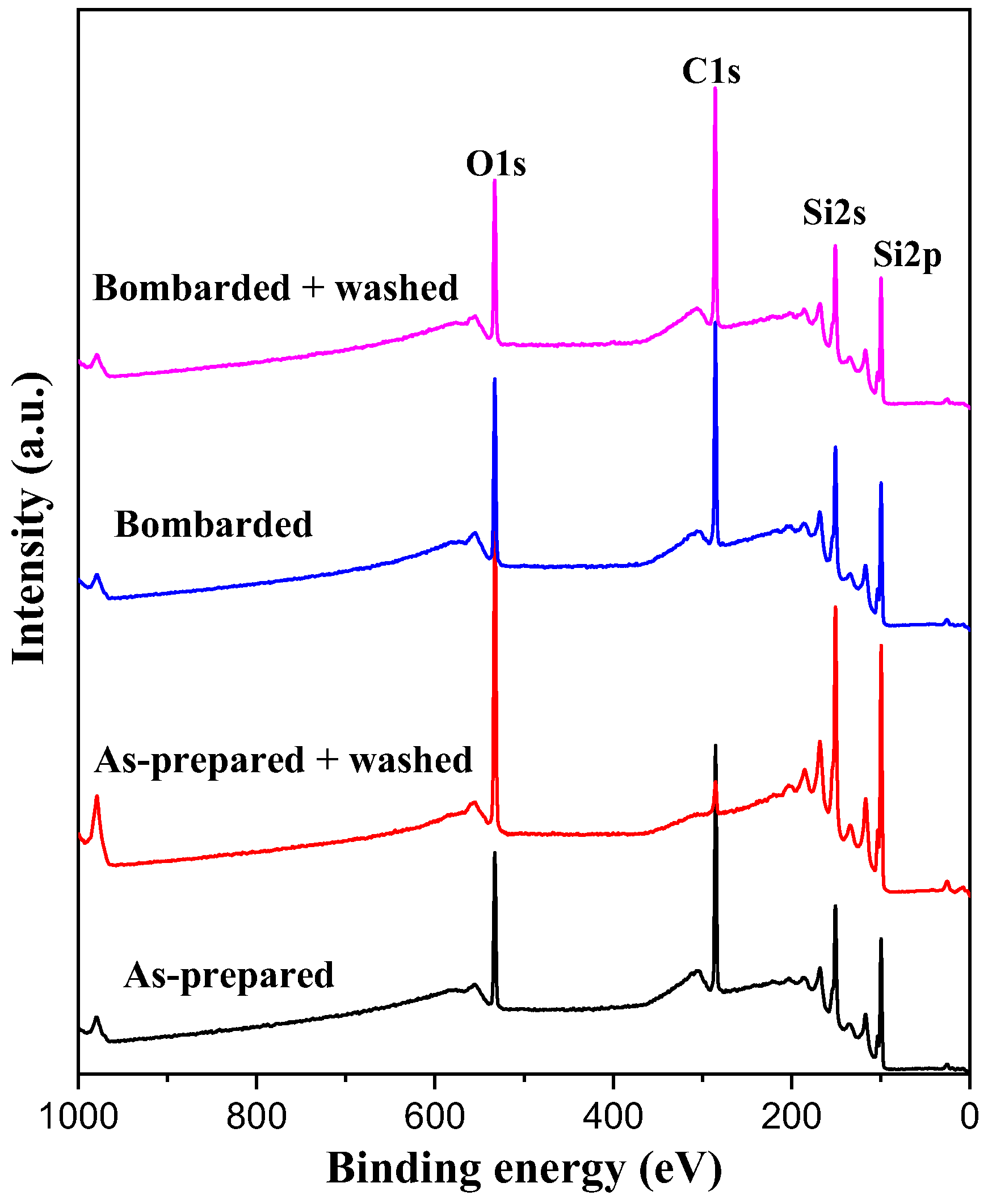
XPS analysis results, both before and after cross-linking induced by bombardment, are shown in Figure 3. A comparison of XPS survey spectra of different treated C32H66 samples clearly showed that the C1s signal became very small for the untreated and hexane-washed case. Here, O1s, Si2p, and Si2s came from substrates in the spectra. There was almost no change in the ratio of C1s to Si2p intensity (peak area) for the cross-linked samples. This was consistent with AFM results. The thickness of the thin film can be approximately estimated by using the C1s to Si2p peak area, following Equation (1):
I C 1 s I S i 2 p = I C 1 s 0 I S i 2 p 0 1 e d / λ S i 2 p e d / λ C 1 s
where I is the peak intensity (peak area) of photoelectron emission, d is thickness of the thin films, and λ is the photoelectron mean free path in the thin films.
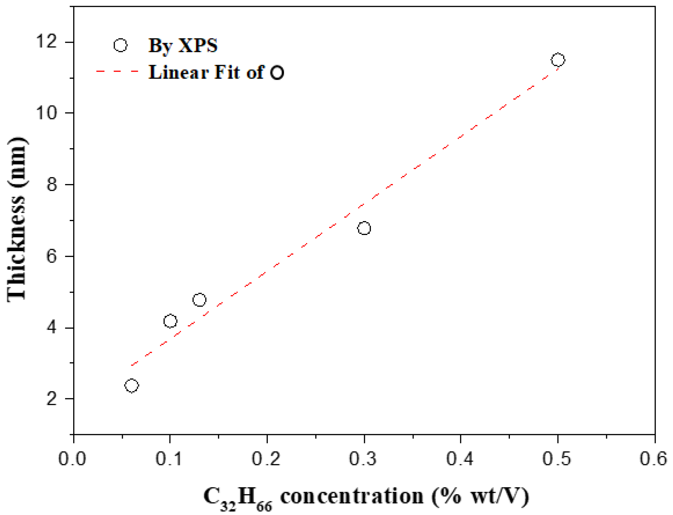
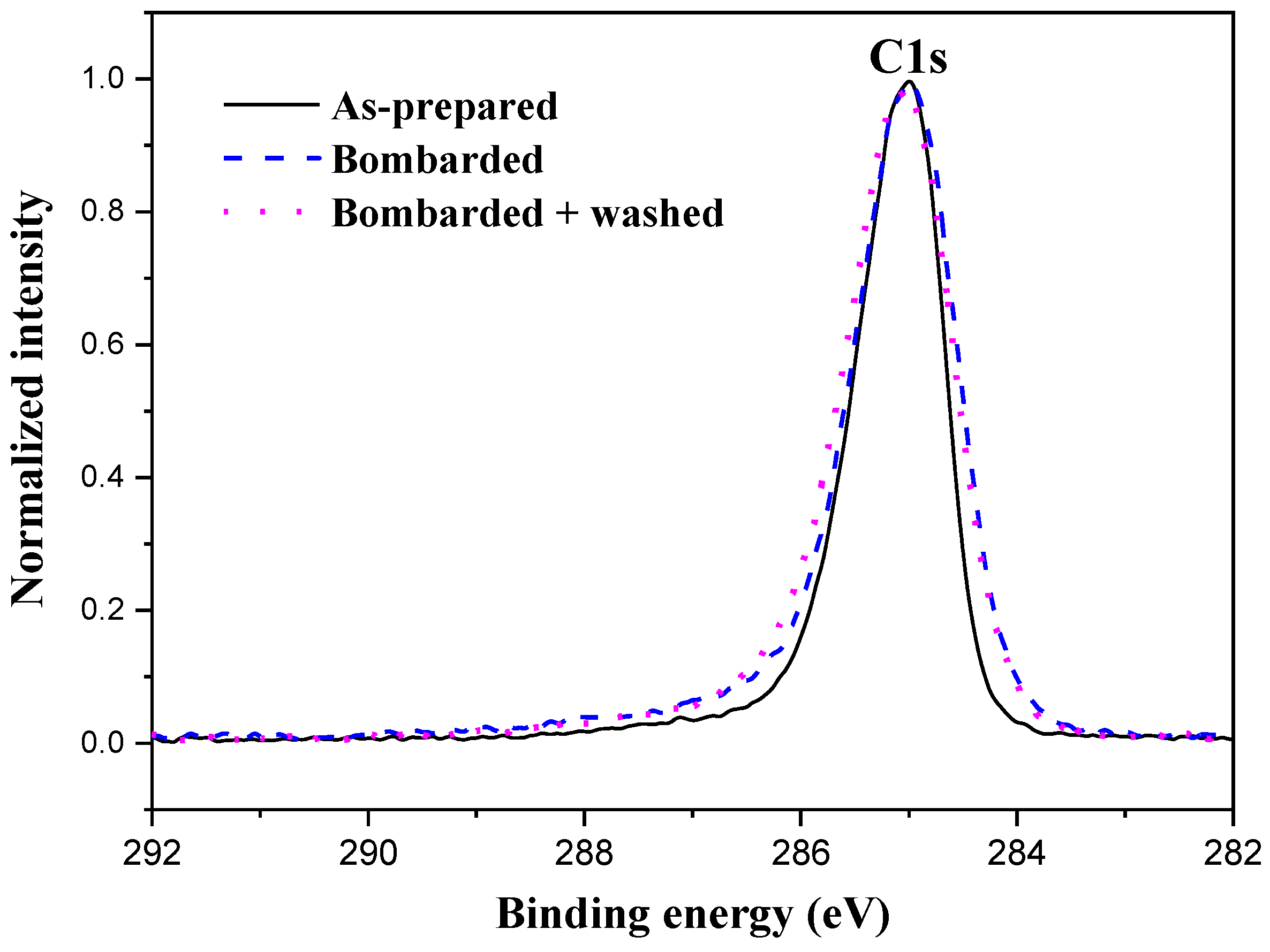
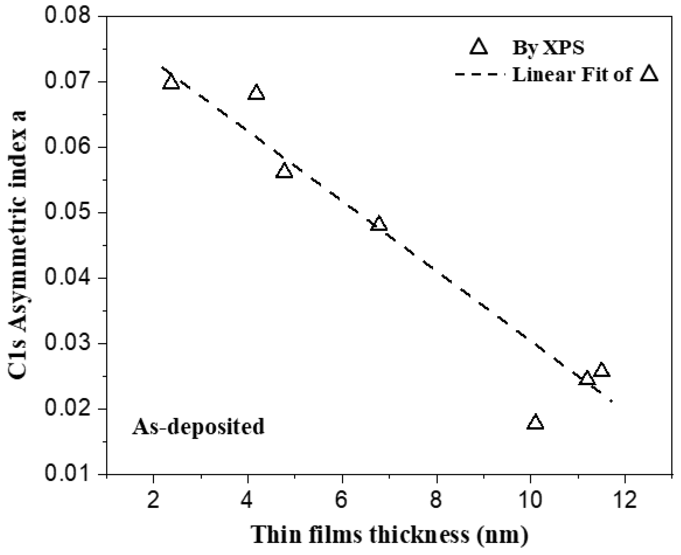
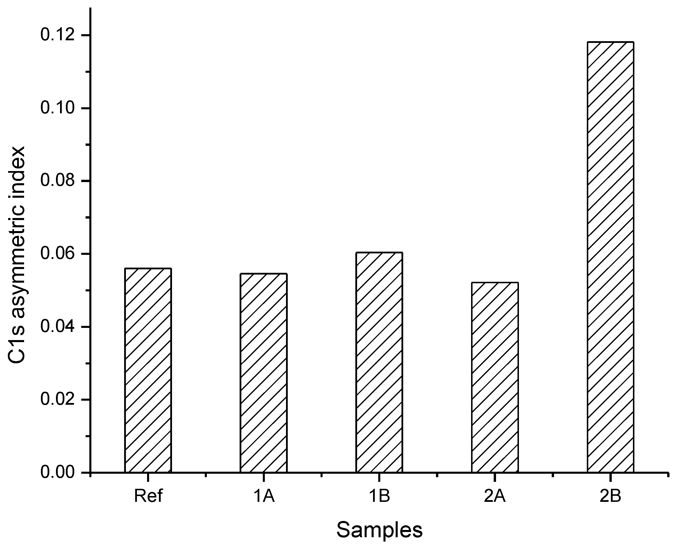
This method was assumed one of the best methods to estimate the thickness of organic molecular layers [24,25,26]. Then, we obtained a relationship of the thickness of thin films as a function of C32H66 concentration. Indeed, the thickness of the thin films was correlated with C32H66 concentration linearly in Figure 4 for a given spin speed. It should be mentioned that the estimation may have had a larger error because Equation (1) supposed that the layer was homogenous in thickness. However, our AFM image indicated that the layer was composed of a perpendicular state (about 4.3 nm thick) and parallel state (about 0.5 nm thick). Therefore, the layer thickness estimation by XPS was an equivalent (or mass) thickness or apparent thickness in a larger analysis area (could be scaled to 100 μm level). It was also noticed that C1s, in Figure 5, an asymmetric peak, showed a slight increase in the peak width after cross-linking. The asymmetric index of C1s, which had been discussed previously, was associated with carbon atomic electronic and crystal structures [27]. The asymmetric index value could be estimated by peak fitting using XPS programs, such as CasaXPS (www.casaxps.com, accessed on 10 May 2022) or XPSPEAK 4.1 (free download is available from the web). More detailed information about it can be found in reference [28]. It was further interesting that the asymmetric index of C1s of the as-deposited thin film showed a decrease with the C32H66 thickness (Figure 6), but it remained constant without any change after full cross-linking except for partial cross-linking and after hexane washing (using a lower bombardment energy through control of the sample position, shown in Figure 7). XPS identified that this sample was only 1 nm thick after C32H66 thin-film cross-linking, confirmed by AFM morphology (see Figure S6). AFM morphology of the sample showed that the vertical molecule feature disappeared and the surface was composed of nanoparticles. The nanoparticles had about a 1 nm height estimated from Figure S6.
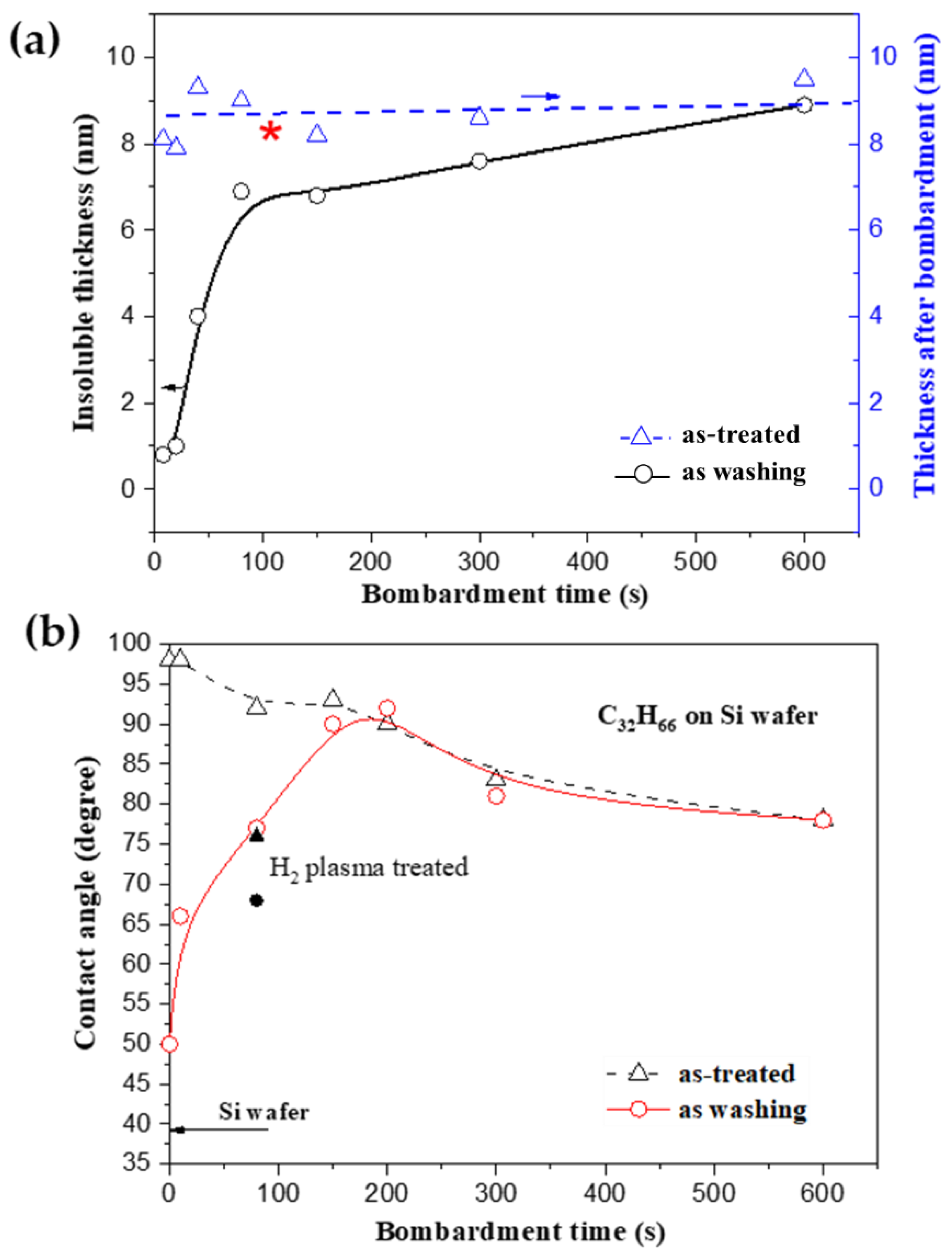
The cross-linking (estimated by the insoluble thickness by hexane washing) of the C32H66 thin films as a function of hyperthermal hydrogen bombardment fluence, for a given hyperthermal hydrogen condition, could be found in Figure 8a, indicating that the insoluble thickness increased with the hyperthermal hydrogen fluence, and the thickness reached a maximum when the fluence was higher than 5 × 10¹⁶/cm2, which was the same as the thickness of hydrogen plasma bombardment-induced cross-linking (red star in the Figure, blue star for the non-plasma-treated sample). The result of Figure 8a also suggested that the film was fully cross-linked after 5 × 10¹⁶/cm2 of hyperthermal hydrogen bombardment. Indeed, the fluence of full cross-linking is dependent on the thickness of the film. It was noted that the higher the full cross-linking, the smaller the thickness of the film.
Herein, we introduced another important surface property—wettability of thin films, to characterize the cross-linking, as shown in Figure 8b. With longer bombardment time, a higher cross-linking caused a smaller contact angle, which was associated with wettability of the top surface of the thin film. It should be noted that the cross-linked thin film prevented the penetration of the moisture onto the top surface of the silicone substrate. The thickness of the insoluble C32H66 films, both as-deposited, treated, and washed, as a function of hyperthermal hydrogen bombardment time found in Figure 8b, indicated that it was fully cross-linked after 200 s of bombardment.
The change in wettability of the thin films surface, both for cross-linked and as-deposited C32H66, can be found in Figure 8b. Except the early stage of the bombardment for the treated and washed cases, the wettability of both surfaces was going to be same. In other words, the water contact angle (WCA) of the washed samples increased with the bombardment time less than 200 s, while the WCA of the unwashed samples slightly decreased within 200 s of bombardment. This might suggest that there was no full cross-linking within 200 s of bombardment. In addition, the lower water contact angle under the shorter bombardment time and washing could be attributed to uncross-linked C32H66 that had been removed and had left the silicon substrate exposed to direct contact with water droplets. The result would lead to the decrease in water contact angle. It was also noted that there was always symmetric water droplets on both the treated and untreated (as-prepared) samples regardless of the thickness. This might suggest that the Si wafer was almost covered by a C32H66 layer even it was in a parallel state, with the result being consistent with the conclusions from Taub’s work [8,18].

4. Discussion

Basically, we have similar AFM images of the C32H66 thin film as Taub’s group [8,18], although they used a different preparation process: (1) a shorter step height (about 3.7 nm) of the first perpendicular layer, which is attributed to the weaker interaction of the cantilever tip to a perpendicular layer (headed by methyl groups) compared to a parallel layer (–CH), and (2) a 4.3–4.5 nm step height for the after-first perpendicular layer. However, we also found that there is a small difference: the step height of two perpendicular layers may not always be with 4.3 nm or its times. It could be 3.3 nm (Figure 1c,d and Figure S1). The tip-molecular group’s interaction mechanism obviously does not work in this case. In fact, it is difficult to believe that there is a significant interaction difference between tip and groups –CH, –CH3. We propose here that the shortening of the step height of the first perpendicular layer may be the reason the first layer is composed of the co-existence of the parallel state and the perpendicular state, rather than the parallel state being underneath the perpendicular state. Then, we can reconstruct the layer structure, as shown in Figure 9, according to the line scanning profile in Figure 1. Then, all the differences in the step height of AFM images can be explained, that is, they are caused by the parallel layer thickness near the perpendicular layer. This is more in line with the model proposed by Riegler et al. [1,2,3,4], the recent simulation from Yamamoto et al. [15], and the experimental results of Nozaki et al. [10].
As mentioned in the previous section, XPS only offers a mass-averaged thickness due to the height difference of co-existing parallel and perpendicular C32H66 layer. We may estimate the average thickness (it should be mass thickness) of the thin films by using the AFM images with the calculated coverage of the parallel layer and perpendicular layer:
d = 0.5 Θ + 4.3 ( 1 Θ )
where Θ is the ratio of the parallel layer (~0.5 nm) to the perpendicular layer (4.3 nm).
For a 0.05% w/v C32H66 thin film, we have an average thickness of 2.1 nm using Equation (2), which agrees well with the 2.4 nm estimated by XPS. It should be noted that the estimation is only limited to very thin layers because there is almost no single parallel layer for the C32H66 concentration more than 0.13% w/v to use AFM measurement. Here, XPS will offer a better estimation result at this case.
The formation of a dendrite feature or fractal characterization is generally caused by limited-diffusion aggregation of C32H66 molecules during the spin-coating process. A systematical evaluation and explanation of the fractal of n-alkane on the SiO2 surface was evaluated by Riegler’s group recently [14].
A linear increase in mass thickness (Figure 4) of the C32H66 as a function of C32H66 concentration indicates that the growth of the C32H66 layer is associated with the concentration, and the thickness of the thin film is controlled by the concentration. This also suggests that the monolayer thickness, even the sub-monolayer-oriented molecular film, can be easily prepared by spin-coating by controlling the speed and C32H66 concentration.
We also find that, the C1s features like the peak width and symmetrychanges during the film deposition and cross-linking, although there are only C-C/C-H bonds, which supposes that they are indistinguishable in the C 1s spectrum. The asymmetric feature of the C 1s peak in n-alkane has been noted previously [29], for example, in hexatriacontane (n-C36H74) carbohydrate, but it has not been completely understood for the peak tail in the high-binding-energy side. Our previous works [27,28,30,31] and others’ [32] have shown that the asymmetric change in the C1s peak in HOPG and carbon nanotubes [28] induced by low-energy ions bombardment can be attributed to the electron states localization of broken C-C bonds and fragments (for example, formation of nanoparticles of a-C [27,28,30,31]) of extensive delocalization of the electron state. Herein, the decrease in asymmetric index and peak width (or full-width at half-maximum, FWHM) upon the thickness of C32H66 may partially be attributed to the decrease in the localized electron state in an individual molecule or more molecules in each layer (both perpendicular and parallel state). Although we know that the crystalline of C32H66 is only involved in the van de Waals interaction with the increase in film thickness, the oriented structure of the C32H66 may share their electrons in the lamellae to delocalize the electron state. Indeed, it is consistent with our AFM result: the partial cross-linking of C32H66, as seen in Figure S6, and the clustering of C32H66 result in the increase in asymmetric index and peak width. This is in good agreement with the XPS results in Figure 7. However, both fully cross-linked and partially cross-linked thin films show a smaller asymmetric index, suggesting that the delocalized electron state both in cross-linked and crystalline C32H66 is similar. A slight increase in asymmetric index (Figure 7) of the film after cross-linking may suggest the formation of amorphous carbon or clustering [27,28,30,31,32], consistent with AFM images where the clustering (Figure 2c,d) of C32H66 is due to cross-linking. The formation of nanoparticles of the cross-linked C32H66 films is in accordance with STM results [33,34] of the cross-linking of SAMs of dodecanethiol on Au(111) induced by hyperthermal proton bombardment.
Although we observe a decrease in the films (in fact, it is average step height of perpendicular lamellae in AFM image) after cross-linking induced by hyperthermal hydrogen bombardment in the AFM image (see Figure S5), we do not note any decrease in the average thickness of the film after fully cross-linking by XPS estimation. It may be ascribed to the decrease in mean free path of the photoelectron in the cross-linked films compared to that in the films without cross-linking, due to the increase in the density of cross-linked films. In addition, some residual solvent is absorbed by the films after using solvent to wash.
The slight decrease in WCA for treated samples may indicate the loss of hydrogen in CH3 to CH or C-C in the top of the molecules due to the cross-linking induced by HHIC. The increase in WCA with bombardment time for the washed treatment within 200 s suggests that the cross-linking induced by HHIC is incomplete during that time. This incomplete cross-linking of the films can be partly washed away by hexane and can leave part of the Si wafer (SiOx) surface exposed to air, which will result in the decrease in the WCA. Moreover, wettability of films after HHIC treatment further supplies more information of the cross-linking process. We note that there is an essential difference in WCA between surfaces treated after hydrogen plasma and HHIC. A lower WCA of the hydrogen plasma-treated surface implies that there may be partial oxidation after hydrogen plasma treatment (increase in surface energy). However, a higher WCA of the surface treated by HHIC indicates that it does not need to be oxidized. This merit can broaden the application field of HHIC.
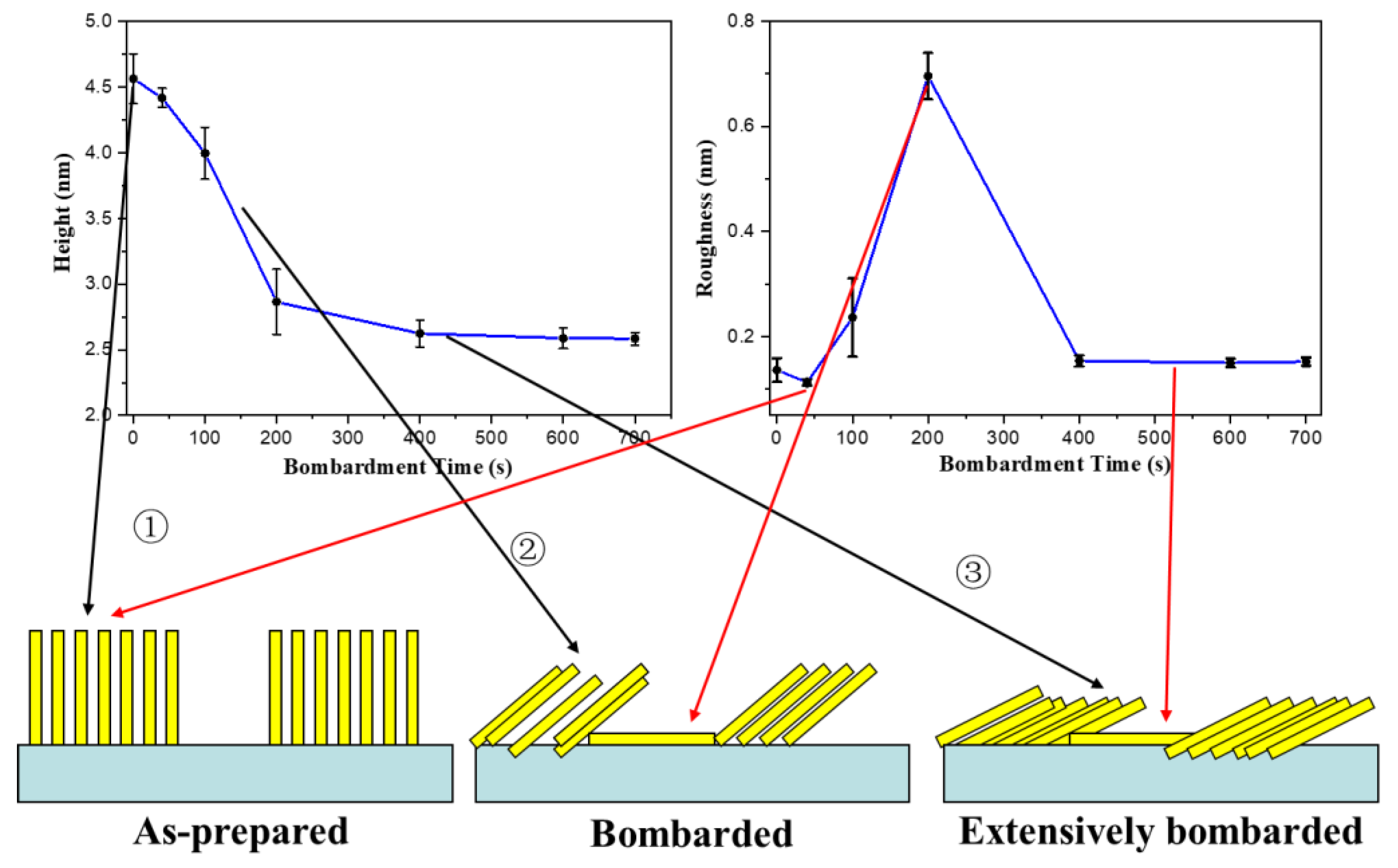
Based on both the above XPS and AFM measurements, we can propose a model of the film growth shown in Figure 9, in which the mixing of the parallel and perpendicular lamellae in the first layer coexists. The cross-linking of the film induced by HHIC can be schematized in Figure 10 based on the AFM measurement both in height and roughness. The cross-linking process of the film can be classified into three stages: oriented molecules for as-deposited; laying-down of the vertical molecules due to the cross-linking and partial clustering; and densely disordered and cross-linked film. Clearly, after full cross-linked fluence (e.g., 5 × 10¹⁶/cm2), the film becomes dense and smooth, consistent with the XPS measurement.

5. Conclusions

Our extensive AFM and XPS analyses show that there is a co-existence of perpendicular and parallel molecular lamellae on the Si wafer surface by spin-coasting under very low C32H66 concentrations. The thin films are dominated by perpendicular state layers, which result in a multilayer structure for higher C32H66 concentration. The monolayer film, composed by the mixing of the mono-parallel and mono-perpendicular layers, has been successfully cross-linked by hyperthermal hydrogen bombardment.

Supplementary Materials

The following supporting information can be downloaded at: https://www.mdpi.com/article/10.3390/app12126233/s1, Figure S1: AFM topography of the C32H66 thin film deposited by 0.3% w/v C32H66 concentration, showing multilayer structures; Figure S2: AFM topography of the C32H66 thin film deposited by 0.3% w/v C32H66 concentration, showing multilayer structures and “bulk particles”, where molecules are perpendicularly oriented; Figure S3: AFM image and two-line profiles of Si wafer surface in noncontact mode; Figure S4: Histogram and bearing ratio estimation from AFM image shown in Figure 1b; Figure S5: AFM image of a fully cross-linked C32H66 thin-film surface induced by hyperthermal hydrogen bombardment and two line profiles; Figure S6: AFM image of a partially cross-linked C32H66 thin-film surface induced by hyperthermal hydrogen bombardment and two line profiles. XPS estimation shows that a 1 nm C32H66 has been cross-linked.

Author Contributions

Methodology, Y.Z. and W.M.L.; formal analysis, H.-Y.N.; investigation, R.X.; resources, W.M.L.; data curation, J.L. and R.X.; writing—original draft preparation, J.L.; writing—review and editing, D.-Q.Y.; funding acquisition, Y.Z. All authors have read and agreed to the published version of the manuscript.

Funding

This research was funded by the National Natural Science Foundation of China (NSFC), Grant No. 21104028 (Yan Zhu), the 2014 Competitive Grant Program of Oversea Returnees Research Project, China National Social Development Grant No. [2014]240 (Yan Zhu), and the Natural Science Foundation of Yunnan Province of China (NSFYPC), Grant No. 2011FZ015 (Yan Zhu).

Data Availability Statement

Not applicable.

Conflicts of Interest

The authors declare no conflict of interest.

References

  1. Fazekas, T.J.; Alty, J.W.; Neidhart, E.K.; Miller, A.S.; Leibfarth, F.A.; Alexanian, E.J. Diversification of aliphatic C–H bonds in small molecules and polyolefins through radical chain transfer. Science 2022, 375, 545–550. [Google Scholar] [CrossRef] [PubMed]
  2. Liu, Y.; Yang, D.Q.; Nie, H.Y.; Lau, W.M.; Yang, J. Study of a hydrogen-bombardment process for molecular cross-linking within thin films. J. Chem. Phys. 2011, 134, 074704. [Google Scholar] [CrossRef] [PubMed]
  3. Schollmeyer, H.; Struth, B.; Riegler, H. Long Chain n-Alkanes at SiO2/Air Interfaces: Molecular Ordering, Annealing, and Surface Freezing of Triacontane in the Case of Excess and Submonolayer Coverage. Langmuir 2003, 19, 5042–5051. [Google Scholar] [CrossRef]
  4. Lazar, P.; Schollmeyer, H.; Riegler, H. Spreading and Two-Dimensional Mobility of Long-Chain Alkanes at Solid/Gas Interfaces. Phys. Rev. Lett. 2005, 94, 116101. [Google Scholar] [CrossRef] [PubMed]
  5. Volkmann, U.G.; Pino, M.; Altamirano, L.; Taub, H.; Hansen, F.Y. High-resolution ellipsometric study of an n-alkane film, dotriacontane, adsorbed on a SiO2 surface. J. Chem. Phys. 2002, 116, 2107–2115. [Google Scholar] [CrossRef] [Green Version]
  6. Mo, H.; Taub, H.; Volkmann, U.; Pino, M.; Ehrlich, S.; Hansen, F.Y.; Lu, E.; Miceli, P. A novel growth mode of alkane films on a SiO2 surface. Chem. Phys. Lett. 2003, 377, 99–105. [Google Scholar] [CrossRef]
  7. Mo, H.; Trogisch, S.; Taub, H.; Ehrlich, S.; Volkmann, U.; Hansen, F.Y.; Pino, M. Structure and growth of dotriacontane films on SiO2 and Ag(111) surfaces: Synchrotron X-ray scattering and molecular dynamics simulations. Phys. Status Solidi A 2004, 201, 2375–2380. [Google Scholar] [CrossRef]
  8. Trogisch, S.; Simpson, M.; Taub, H.; Volkmann, U.G.; Pino, M.; Hansen, F.Y. Atomic force microscopy measurements of topography and friction on dotriacontane films adsorbed on a SiO2 surface. J. Chem. Phys. 2005, 123, 154703. [Google Scholar] [CrossRef] [Green Version]
  9. Kruchten, F.; Knorr, K.; Volkmann, U.G.; Taub, H.; Hansen, F.Y.; Matthies, B.; Herwig, K.W. Ellipsometric and neutron diffraction study of pentane physisorbed on graphite. Langmuir 2005, 21, 7507–7512. [Google Scholar] [CrossRef]
  10. Nozaki, K.; Saihara, R.; Ishikawa, K.; Yamamoto, T. Structure of Normal Alkane Evaporated Films: Molecular Orientation. Jpn. J. Appl. Phys. 2007, 46, 761–769. [Google Scholar] [CrossRef] [Green Version]
  11. Jandt, K.; Miles, M.; Petermann, J.; Thomson, N. STM investigations of an alkane-metal-system (C32H66/In). Polym. Bull. 1994, 33, 687–691. [Google Scholar] [CrossRef]
  12. Espeau, P.; Reynolds, P.A.; Dowling, T.; Cookson, D.; White, J.W. X-Ray diffraction from layers of n-alkanes adsorbed on graphite. J. Chem. Soc. Faraday Trans. 1997, 93, 3201–3208. [Google Scholar] [CrossRef]
  13. Basu, S.; Satija, S. In-situ X-ray reflectivity study of alkane films grown from the vapor phase. Langmuir 2007, 23, 8331–8335. [Google Scholar] [CrossRef]
  14. Knüfing, L.; Schollmeyer, H.; Riegler, H.; Mecke, K. Fractal analysis methods for solid alkane monolayer domains at SiO2/air interfaces. Langmuir 2005, 21, 992–1000. [Google Scholar] [CrossRef]
  15. Yamamoto, T.; Nozaki, K.; Yamaguchi, A.; Urakami, N. Molecular simulation of crystallization in n-alkane ultrathin films: Effects of film thickness and substrate attraction. J. Chem. Phys. 2007, 127, 154704. [Google Scholar] [CrossRef] [PubMed]
  16. Hess, G.B. Phase Transitions in Surface Films 2. NATO Adv. Study Inst. N. Y. 1991, 267, 357–389. [Google Scholar]
  17. Li, Z.; Gorp, H.V.; Walke, P.; Phan, T.H.; Fujita, Y.; Greenwood, J.; Ivasenko, O.; Tahara, K.; Tobe, Y.; Uji-I, H.; et al. Area-selective passivation of sp2 carbon surfaces by supramolecular self-assembly. Nanoscale 2017, 9, 5188–5193. [Google Scholar] [CrossRef] [PubMed]
  18. Bai, M.; Trogisch, S.; Magonov, S.; Taub, H. Explanation and correction of false step heights in amplitude modulation atomic force microscopy measurements on alkane films. Ultramicroscopy 2008, 108, 946–952. [Google Scholar] [CrossRef] [PubMed]
  19. Mo, H.; Trogisch, S.; Taub, H.; Ehrlich, S.; Volkmann, U.G.; Hansen, F.Y.; Pino, M. Studies of the structure and growth mode of dotriacontane films by synchrotron x-ray scattering and molecular dynamics simulations. J. Phys. Condens. Matter 2004, 16, S2905. [Google Scholar] [CrossRef] [Green Version]
  20. Trebicky, T.; Crewdson, P.; Paliy, M.; Bello, I.; Nie, H.Y.; Zheng, Z.; Fan, X.L.; Yang, J.; Gillies, E.R.; Tang, C.Y.; et al. Cleaving C–H bonds with hyperthermal H2: Facile chemistry to cross-link organic molecules under low chemical- and energy-loads. Green Chem. 2014, 16, 1316–1325. [Google Scholar] [CrossRef]
  21. Zheng, Z.; Xu, X.D.; Fan, X.L.; Lau, W.-M.; Kwok, R.W.M. Ultrathin polymer film formation by collision-induced cross-linking of adsorbed organic molecules with hyperthermal protons. J. Am. Chem. Soc. 2004, 126, 12336–12342. [Google Scholar] [CrossRef] [PubMed]
  22. Zheng, Z.; Kwok, W.M.; Lau, W.M. A new cross-linking route via the unusual collision kinematics of hyperthermal protons in unsaturated hydrocarbons: The case of poly(trans-isoprene). Chem. Commun. 2006, 29, 3122–3124. [Google Scholar] [CrossRef] [PubMed]
  23. Zheng, Z.; Wong, K.W.; Lau, W.C.; Kwok, R.W.M.; Lau, W.M. Unusual Kinematics-Driven Chemistry: Cleaving C-H but Not COO-H Bonds with Hyperthermal Protons To Synthesize Tailor-Made Molecular Films. Chem.-A Eur. J. 2007, 13, 3187–3192. [Google Scholar] [CrossRef] [PubMed]
  24. Laibinis, P.E.; Bain, C.D.; Whitesides, G.M. Attenuation of Photoelectrons in Monolayers of n-Alkanethiols Adsorbed on Copper, Silver and Gold. J. Phys. Chem. 1991, 95, 7017–7021. [Google Scholar] [CrossRef]
  25. Lamont, C.L.; Wilkes, J. Attenuation Length of Electrons in Self-Assembled Monolayers of n-Alkanethiols on Gold. Langmuir 1999, 15, 2037–2042. [Google Scholar] [CrossRef]
  26. Wallart, X.; Henry de Villeneuve, C.; Allongue, P. Truly Quantitative XPS Characterization of Organic Monolayers on Silicon: Study of Alkyl and Alkoxy Monolayers on H-Si(111). J. Am. Chem. Soc. 2005, 127, 7871–7878. [Google Scholar] [CrossRef]
  27. Yang, D.-Q.; Sacher, E. Carbon 1s X-ray photoemission line shape analysis of highly oriented pyrolytic graphite: The influence of structural damage on peak asymmetry. Langmuir 2006, 22, 860–862. [Google Scholar] [CrossRef]
  28. Yang, D.-Q.; Sacher, E. Ar+-induced surface defects on HOPG and their effect on the nucleation, coalescence and growth of evaporated copper. Surf. Sci. 2002, 516, 43–55. [Google Scholar] [CrossRef]
  29. Beamson, G.; Briggs, D. High Resolution XPS of Organic Polymers: The Scienta ESCA300 Database; Wiley: New York, NY, USA, 1992; pp. 125–148. [Google Scholar]
  30. Yang, D.-Q.; Sacher, E. s–p Hybridization in highly oriented pyrolytic graphite and its change on surface modification, as studied by X-ray photoelectron and Raman spectroscopies. Surf. Sci. 2002, 504, 125–137. [Google Scholar] [CrossRef]
  31. Yang, D.-Q.; Rochette, J.-F.; Sacher, E. Controlled Chemical Functionalization of Multiwalled Carbon Nanotubes by Kiloelectronvolt Argon Ion Treatment and Air Exposure. Langmuir 2005, 21, 8539–8545. [Google Scholar] [CrossRef]
  32. Speranza, G.; Minati, L.; Anderle, M. The C1s core line in irradiated graphite. J. Appl. Phys. 2007, 102, 043504. [Google Scholar] [CrossRef]
  33. Xi, L.; Zheng, Z.; Lam, N.-S.; Grizzi, O.; Lau, W.-M. Effects of hyperthermal proton bombardment on alkanethiol self-assembled monolayer on Au(1 1 1). Appl. Surf. Sci. 2007, 254, 113–115. [Google Scholar] [CrossRef]
  34. Xi, L.; Zheng, Z.; Lam, N.-S.; Nie, H.-Y.; Grizzi, O.; Lau, W.-M. Study of the Hyperthermal Proton Bombardment Effects on Self-Assembled Monolayers of Dodecanethiol on Au(111). J. Phys. Chem. C 2008, 112, 12111–12115. [Google Scholar] [CrossRef]
Figure 1. AFM images and two representative profiles isolated from the images of C32H66 thin films deposited with different concentrations on the substrate. (a) 0.05% w/v, (b) 0.13% w/v, (c) 0.3% w/v, and (d) 0.5% w/v.
Applsci 12 06233 g001
Figure 2. AFM images of C32H66 thin films prepared at the concentration of 0.13% w/v (a) as-deposited, (b) as-deposited and hexane-washed, (c) after hyperthermal hydrogen bombardment cross-linking, and (d) after hyperthermal hydrogen bombardment and hexane washing (insets: their higher-resolution images and scanning scale is 1 μm × 1 μm).
Applsci 12 06233 g002
Figure 3. Comparisons of XPS survey spectra of C32H66 thin film prepared at the concentration of 0.3% w/v after different surface treatments.
Applsci 12 06233 g003
Figure 4. Thickness of C32H66 thin films estimated from the XPS intensities as a function of its spin coating concentration.
Applsci 12 06233 g004
Figure 5. Comparisons of C1s of C32H66 thin films prepared at the concentration of 0.3% w/v after hyperthermal hydrogen bombardment, indicating increase in peak width after cross-linking induced by the bombardment.
Applsci 12 06233 g005
Figure 6. Thickness of as-prepared C32H66 thin film effects on the C1s asymmetric index.
Applsci 12 06233 g006
Figure 7. Cross-linking of C32H66 thin films induced by hyperthermal hydrogen bombardment effects on C1s peak asymmetric index, prepared at a concentration of 0.3% w/v. Ref: as-prepared thin film. 1A and 1B: fully cross-linked C32H66 after the bombardment and hexane washing, respectively. 2A and 2B: partially cross-linked C32H66 films (about 25% cross-linking) and hexane-washing, respectively.
Applsci 12 06233 g007
Figure 8. Insoluble thickness of the C32H66 thin films prepared at the concentration of 0.3% w/v, as a function of hyperthermal bombardment fluence (a); effect of hydrogen bombardment on wettability of thin film surface (b). * represents the thickness after 100 s of H plasma treatment (plasma fluence is not measured), and ▲ and ● represent the thin films after same treatment, with and without hexane-washing, respectively.
Applsci 12 06233 g008
Figure 9. A proposed C32H66 layer structure of two oriented molecules based on AFM line scanning profile of Figure 1. The model fit for low C32H66 concentration deposition.
Applsci 12 06233 g009
Figure 10. Proposed cross-linking processes of the film during HHIC, as confirmed by AFM images of measured height and roughness change for different process of the cross-linking.
Applsci 12 06233 g010
Publisher’s Note: MDPI stays neutral with regard to jurisdictional claims in published maps and institutional affiliations.