Article

Dual-Boost Inverter for PV Microinverter Application—An Assessment of Control Strategies

1
Department of Engineering Sciences, Universidad Andres Bello, Santiago 7500971, Chile
2
Electronics Engineering Department, Universidad Técnica Federico Santa María, Valparaíso 2390123, Chile
3
Faculty of Engineering Sciences, Universidad Austral de Chile, Valdivia 5110566, Chile
4
Faculty of Engineering, Universidad San Sebastian, Santiago 8420524, Chile
*
Author to whom correspondence should be addressed.
Appl. Sci. 2022, 12(12), 5952; https://doi.org/10.3390/app12125952
Submission received: 6 May 2022 / Revised: 29 May 2022 / Accepted: 6 June 2022 / Published: 11 June 2022
(This article belongs to the Special Issue Contributions to Modeling and Control of Power Electronic Converters)

Abstract

:
Photovoltaic (PV) microinverters have grown rapidly in the small-scale PV market, where typical two-stage converters are used to connect one PV module to the single-phase AC grid. This configuration achieves better performance in terms of energy yield compared with other PV configurations. However, the conversion efficiency of a two-stage system is the main drawback, especially when a high-voltage gain effort is required. In this context, single-stage microinverter topologies have been recently proposed since only one power conversion stage is required to extract the maximum power of the PV module and inject the AC power to the grid. This single-stage configuration allows considerable improvement of the overall efficiency of microinverters by reducing the number of elements in the system. However, the main challenge of these topologies is their control, since all variables of the converter are composed by the AC waveform with DC-bias. In this paper, four control strategies are analyzed for the mainstream single-stage topology, which is the dual-boost inverter (DBI). Classical linear control and three non-linear strategies, namely finite control set–model predictive control, flatness-based control, and sliding mode control, are detailed. The main contribution of this work is a complete comparison of the control strategies, to give insights into the most suitable control strategy for the DBI in PV microinverter application.

1. Introduction

The demand for solar energy has increased rapidly in the last few years, turning it into the most competitive option in electricity generation. The large-scale projects are the mainstream market, which provide an important percentage of the annual installed PV power capacity. On the other hand, the residential, commercial, and industrial rooftop solar systems are also growing in the photovoltaic (PV) market, as reported in the latest analysis by [1], where the global PV microinverter market was valued at USD 1166.24 million in 2019, and it is expected to reach USD 2934.86 million by 2025 (a compound annual growth rate (CAGR) of 24.32%).
In rooftop PV systems, the share of the PV microinverter configurations is increasing, due to the maximum power point tracking (MPPT) being fully distributed among all modules of the PV system, reducing the impact of orientation, partial shading, and module mismatch, thus increasing the energy yield of the PV system.
Although the microinverter configuration, also known as the AC module, presents several advantages, the efficiency of the power converter is the main drawback, having the lowest efficiency among all PV system configurations (central, string, and multi-string configurations). In order to solve this issue, different types of topologies for the power converters have been proposed in the academic and industrial fields. Several of these PV microinverters were reviewed in [2,3,4,5].
In the last few years, some research has focused on single-stage topologies since only one power stage is necessary to control the grid current and perform the MPPT, thus allowing increasing the efficiency. Among these single-stage topologies, the most common solution is the differential mode connection of two bidirectional DC–DC converters. The concept of the single-stage differential inverter is shown in Figure 1, where the output of each DC–DC converter is composed by a sinusoidal waveform with a DC-bias. The differential connection allows canceling the DC-bias, obtaining only the AC component at the output voltage. Differential inverters can be formed by any DC–DC converter topology; thus, the presence of galvanic isolation is optional and depends on the selected DC–DC converter topology. The dual-boost inverter (DBI), originally introduced in [6], is one of the most popular topologies of this type of connection. The power circuit of the DBI consists of two bidirectional DC–DC boost converters.
The biggest underlying problems for single-stage topologies are the restrictions and challenges that arise from the control perspectives. In fact, these topologies are very difficult to control, because the operation point of each DC–DC converter presents large variations, making the linearization process a difficult task. Additionally, each variable of the inverter, including the duty cycle, is composed by DC and AC components.
Since the DBI appeared in the 9090s [6], several control strategies have been proposed and developed in the academic field. These control strategies can be classified into two families, depending on the switching strategy: individual boost converter switching strategy and global switching strategy. In the first family, each DC–DC converter is controlled to generate a sinusoidal output voltage with a DC-bias, as shown in Figure 2a. Note that the output voltage of each DC–DC converter is independent of the output voltage of the inverter. The output current or voltage of the inverter is the main control objective in the second family, as seen in Figure 2b.
The approach in the first family consists of controlling independently each boost converter (converters 1 and 2 of Figure 1) within the inverter, which has been achieved with linear and non-linear methods. The most popular strategy uses a cascaded linear control scheme, where the control objectives are the inductor’s current (inner loop) and the output capacitor’s voltage (external loop) for each boost converter. Two proportional–integral (PI) controllers are used to regulate the inductor’s current and capacitor’s voltage errors, as shown in [7,8,9]. However, the main issue with the PI controller in this application is the steady-state errors and phase shifts associated with controlling sinusoidal variables. Based on this idea, proportional resonant (PR) controllers have been implemented in the control scheme to solve the PI controller problems [10,11]. In addition, non-linear control techniques have been also proposed to regulate individually each boost converter. The first control proposal for this inverter was sliding mode control by Caceres and Barbi [12], where the switching surface is formed by the error of the output capacitor voltage and inductor current of each boost converter. In [13], a dynamic linearizing modulator was employed to control the output capacitor voltage. The differential flatness theory was used to obtain a sinusoidal voltage on the output of each boost converter, through the regulation of the energy stored in the capacitor and inductor [14]. Another non-linear strategy is finite control set–model predictive control (FCS–MPC), which was proposed in [15]. In this strategy, the discrete model of the DBI is used to predict the behavior of the output capacitor’s voltage, inductor’s current, and AC output current. Then, an optimization algorithm is adopted to select the best control action for each boost converter.
On the other hand, the sinusoidal output voltage or current of the inverter ( υ o or i o ) is the main control goal of the second family, where the sliding mode approach has been proposed to achieve these objectives. In [16,17], a sliding mode control strategy based on the indirect regulation of the output voltage through the control of the difference between the inductor’s current was presented. The control scheme is composed by two loops, which regulate the output voltage error of the inverter using a PI controller (external loop) and the difference between the inductor’s current through sliding mode control (internal loop). Two strategies to control the output (AC) current were proposed in [18,19]. In the first work, the control scheme was composed by two loops considering a fixed input voltage for the DBI. The external control loop regulates the output (AC) current, and this loop is based on the PR controller, where an integral term is inserted to avoid a DC component in the output current of the inverter. Additionally, a phase compensator was introduced in this control loop to increase the controller’s phase margin. Then, the internal control loop regulates the difference between the inductor’s current. In [19], the control goal was also the regulation of the inverter’s output current, considering the inverter as a whole system with PV panels in the input. A control scheme composed by three cascaded loops was proposed, where a current mode control was used in the inner loop to regulate the difference between the inductor currents. The next loop is composed by a type III compensator for controlling the grid current, and the external loop regulates the PV (input) voltage through a PI controller. One advantage of controlling the system as a whole (inverter) and not independently (each DC–DC boost converter) is the reduction of the amount of control loops, which decreases the number of required sensors.
Additionally, the grid connection of this inverter is another big challenge because finding a direct relationship between the output current and control variables is difficult. In [10,11,18,20,21,22], the experimental validation of the DBI with grid connection was performed. A linear control strategy to regulate the output voltage of each DC–DC converter was used in [11,20]. Furthermore, an active and reactive power control was incorporated in the cascaded scheme, which presents five control loops in total to incorporate the inverter with the grid, generating a complicated design of the control strategy. In [22], three types of voltage modulators were presented and implemented; symmetric (control of each DC–DC converter), asymmetric (control of the whole system), and passivity-based (based on the control of each DC–DC converter) modulators. According to these results, the control based on passivity-based modulation presented the best output current tracking performance, because the control strategy considers the output current, the DC component of the output current, and the output voltage of each DC–DC converter. This control scheme is composed of three loops: a DC component compensator to reduce or eliminate the DC-bias presented in the output voltage of each DC–DC converter, a PR controller with a voltage drop compensator to regulate the output voltage, and the passivity-based modulation strategy. A summary of the aforementioned control strategies is shown in Table 1.
In this context, this work proposes an analysis and comparison of four control strategies for grid-connection of the DBI topology. In particular, the classical linear approach [11,23] and three non-linear strategies are considered: finite control set–model predictive control (FCS–MPC) [15], flatness-based control [14], and sliding mode control [18]. The remainder of the paper is organized as follows. A detailed description of the DBI topology and its modeling are presented in Section 2. The details of the control strategies selected in the comparison are introduced in Section 3. The comparison of the results is presented in Section 4, and Section 5 presents the main conclusions and accomplishments of this paper.

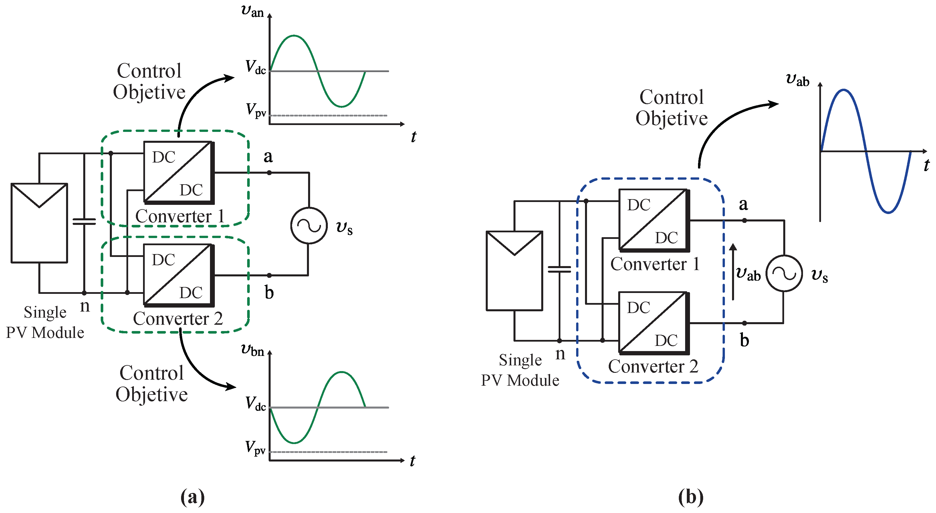
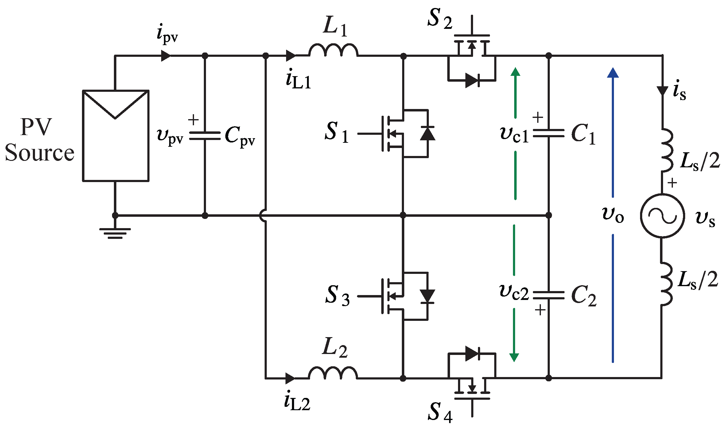
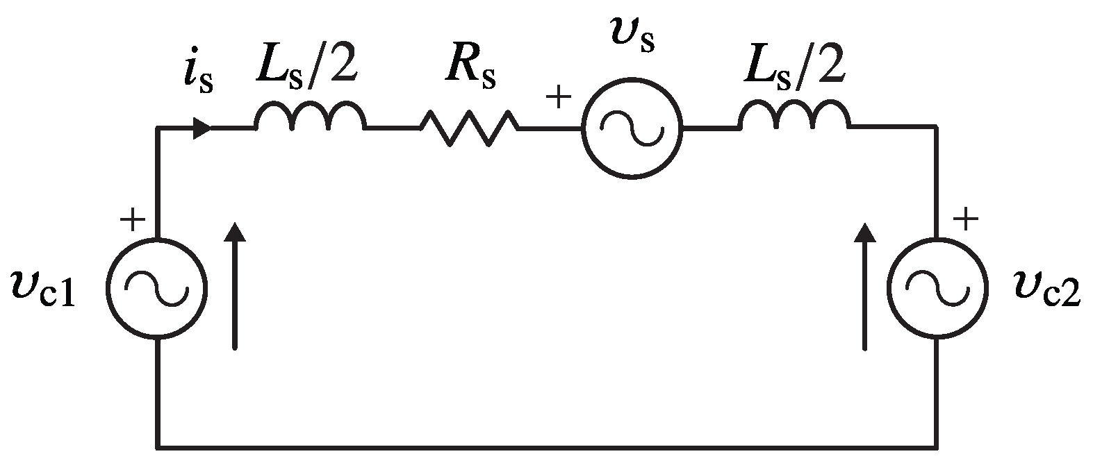
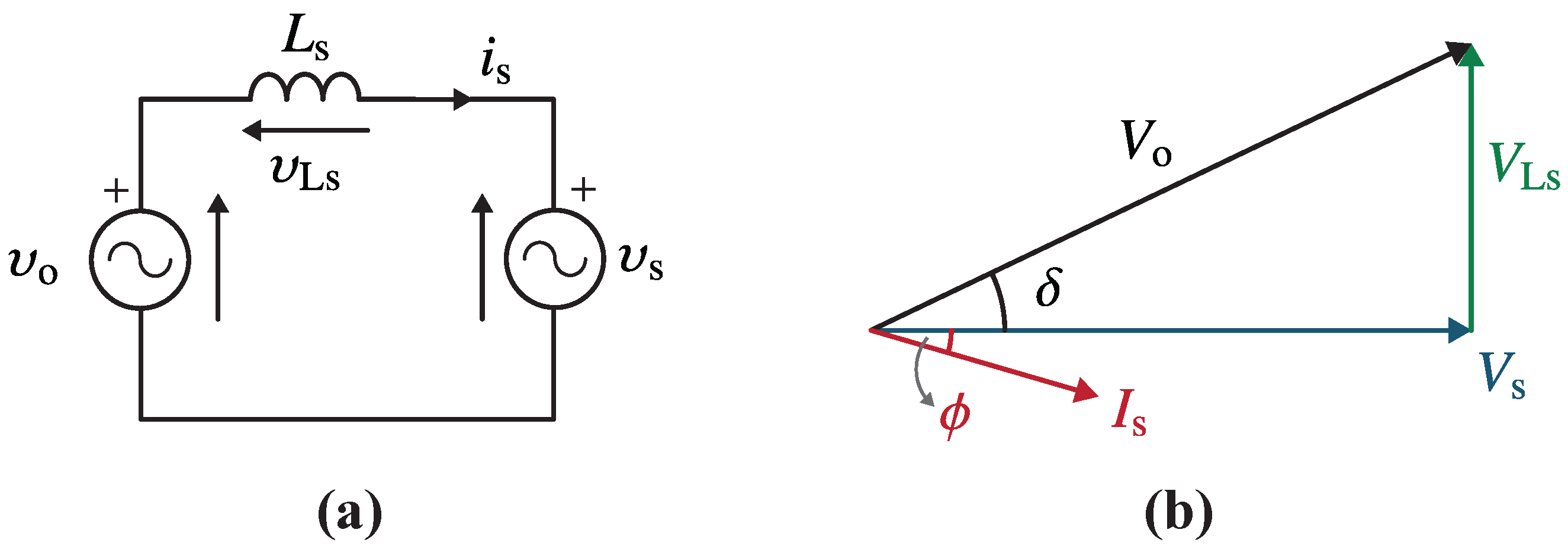
2. Operation and Modeling of the DBI

The DBI is composed by two DC–DC bidirectional boost converters, sharing the input source (PV panel), as illustrated in Figure 3. Note that both boost converters operate in a non-conventional manner; indeed, each boost generates a low-frequency (60 Hz) AC output voltage with a DC-bias. In order to obtain only an AC output, a differential connection between both boost converters (upper terminal of each boost’s output capacitor) is performed. Moreover, a π / 2 phase shift between the AC components (and having the same DC-bias) allows eliminating the DC-bias while duplicating the AC component. As can be observed, the inverter presents four semiconductors, two inductors on the input and two capacitors in the output. The grid is connected between the positive nodes of the output of each boost converter, i.e., differential connection.
The operation of the converter and related control depends on the adopted control strategy. In this work, two different switching strategies are considered. Indeed, the operation of the DBI can be defined by considering individual operation of each boost converter [7]. On the other hand, it is possible to use a second switching strategy, by considering a global scheme for the whole structure [17]. The two switching strategies are detailed in the following section, and a model of each operation is deduced.

2.1. Individual Boost Converter Switching Strategy

In this case, each boost converter is operated individually through switching signals S 1 and S 3 ( S 2 and S 4 being their respective complementary). As summarized in Table 2, the four possible switching states result in eight conduction states depending on the grid current polarity.
Considering the operation of the inverter, the averaged model is described by:
Boost converterx:
L x d i Lx ( t ) d t = υ pv υ cx ( t ) ( 1 d x ( t ) )
C x d υ cx ( t ) d t = ( 1 d x ( t ) ) i Lx ( t ) i s ( t )
where x is 1 or 2, depending on boost converter 1 or 2, i Lx is the current through the inductor L x , i s is the grid current, υ cx is the voltage of the output capacitors, υ pv is the input voltage, and d x ( t ) is the duty cycle of boost converter x.
Moreover, the DBI is integrated with the grid through an inductive filter L s ( R s being its equivalent resistance), as shown in Figure 4. The differential voltage equation can be obtained by
L s d i s ( t ) d t = υ o ( t ) i s ( t ) R s υ s ( t )
where the output voltage of the inverter is defined as
υ o ( t ) = υ c 1 ( t ) υ c 2 ( t )
In general, the output voltage of the inverter is a sinusoidal waveform, which is generated through the difference between the voltage output of each boost converter. These outputs do not necessarily have to be sinusoidal, as long as the difference between them is a sinusoidal output.
In this case, the output of each DC–DC converter is chosen as a sinusoidal output voltage with a DC-bias ( V DC required for proper operation as boost), as shown below:
υ c 1 ( t ) = V DC + V s 2 sin ω s t + δ
υ c 2 ( t ) = V DC V s 2 sin ω s t + δ

2.2. Global Switching Strategy

For the implementation of the global switching strategy for the whole inverter shown in Figure 3, the power devices S 1 and S 4 are controlled with the same gating signal u ( t ) , while the other diagonal power devices ( S 2 and S 3 ) are controlled with the complementary gating signal 1 u ( t ) , then defining the global operation of the system. The averaged model of the DBI is in this case described by
L 1 d i L 1 ( t ) d t = υ pv υ c 1 ( t ) ( 1 u ( t ) )
L 2 d i L 2 ( t ) d t = υ pv υ c 2 ( t ) u ( t )
C 1 d υ c 1 ( t ) d t = ( 1 u ( t ) ) i L 1 ( t ) + i s ( t )
C 2 d υ c 2 ( t ) d t = u ( t ) i L 2 ( t ) i s ( t )
Similar to the previous case, the DBI is connected to the grid through an inductive filter L s ( R s represents the resistance of the inductive filter), as illustrated in Figure 4.

3. Control Strategies of the DBI

As shown in the previous section, for both switching strategies, the resulting operation and modeling present non-linearities, the grid current is not directly associated with the control signal, and a fourth-order system is obtained in the global switching case. Consequently, the main challenge of the DBI is the design of its control.

3.1. Selected Control Strategies
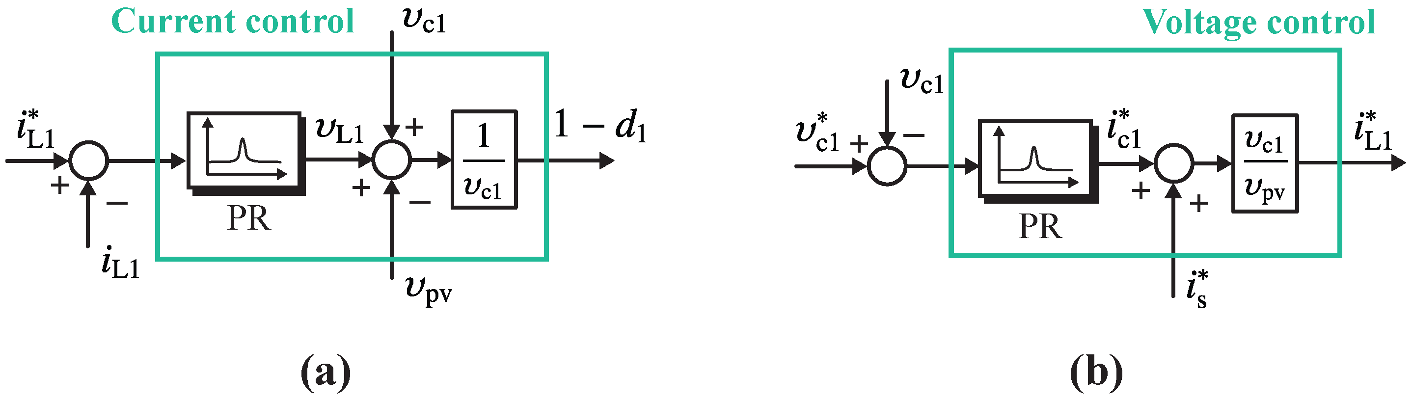
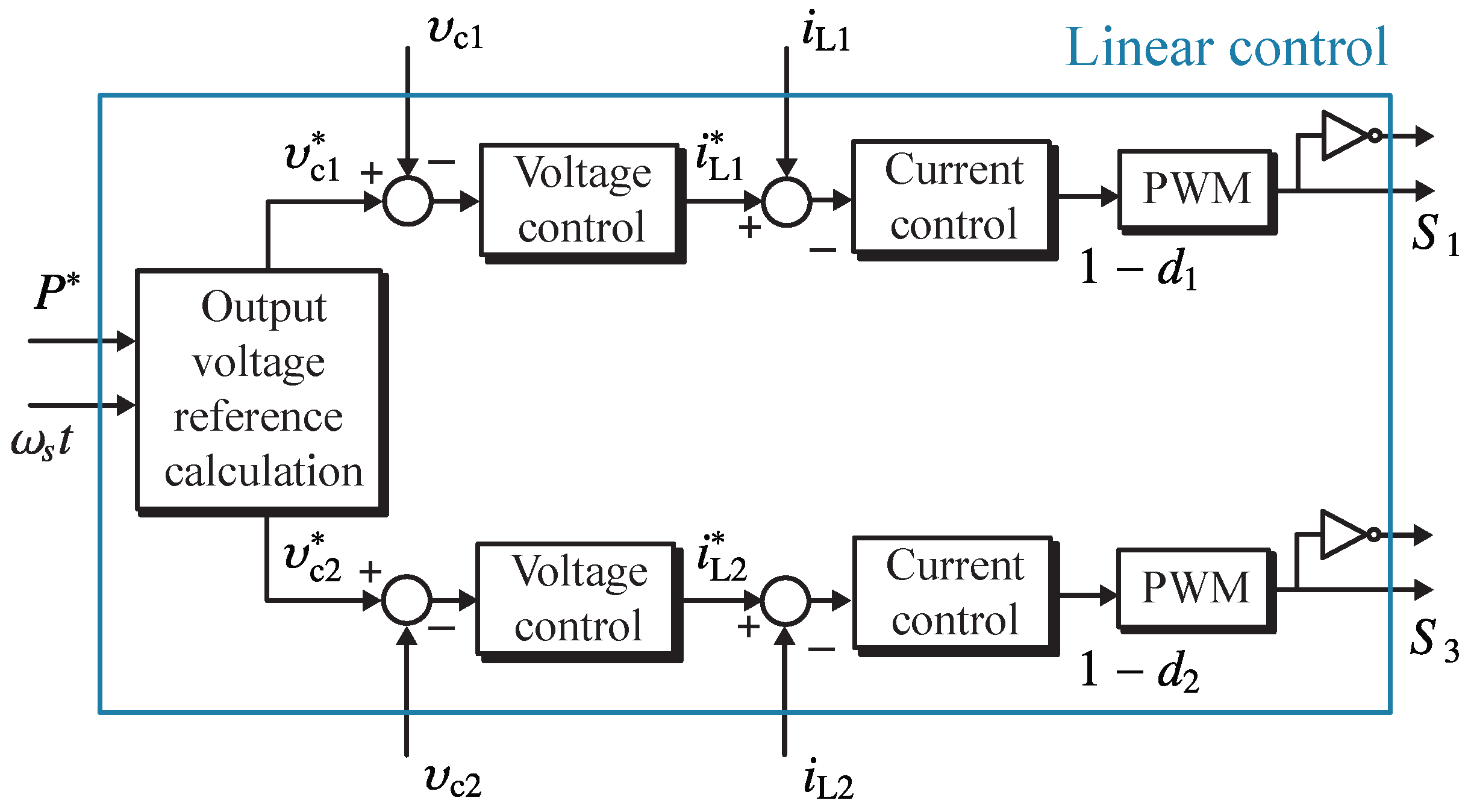
This work presents a comparison among the possible control strategies of the DBI. In particular, four control strategies were selected, including a classical linear control scheme and three non-linear control strategies, namely FCS–MPC, flatness-based control, and sliding mode control. Linear control is a widely used strategy in the industry since the implementation and design are well known and simple. For these reasons, linear control was selected as one of the strategies to be analyzed. The reminder of the control strategies to be analyzed in this document were selected based on their qualities in terms of (control) robustness, fast dynamic performance, and flexibility to incorporate restrictions and constraints, among others. Furthermore, the development of microprocessor technology has enabled the use of advanced control strategies [24]; therefore, FCS–MPC, flatness-based control, and sliding mode control were selected as additional control strategies to be analyzed.
The general control diagram of the four strategies for the DBI is presented in Figure 5. Since a PV module is used as the input source, the four control schemes are composed by a common part, which is the maximum power point tracking (MPPT) of the PV module and the PV voltage control. In order to obtain the maximum power output of the PV panel, the conventional perturb and observe (P&O) algorithm was implemented in the four control schemes due to its simplicity and effective tracking [25].
In order to regulate the voltage of the input capacitor, the PI controller was used. The reference of the PV voltage υ pv * is obtained from the MPPT algorithm. Then, the second-order harmonic in the PV voltage measurement υ pv , inherent to single-phase inverters, is attenuated by the notch filter.

3.2. Linear Control

The linear control scheme is based on the approach presented in [7,23], where the individual DC–DC converter control strategy is used. For this reason, the explanation of the structure control is presented only for one boost converter.
Each boost converter is regulated by two cascaded control loops, as shown in Figure 6, which include compensations to achieve the variable operation of the inverter. The inner control loop regulates the inductor current, while the external control loop regulates the output capacitor voltage. Both control loops are composed by a proportional resonant (PR) controller since the reference of the capacitor voltage control loop is a sinusoidal waveform, and this type of controller tracks sinusoidal references with zero steady-state error [26]. Each stage of the control scheme is described as follows.
Output voltage reference calculation: The active and reactive power transfer between the DBI and grid can be calculated through the model of the grid connection of the inverter and the equivalent complex phasor [27,28]. In this analysis, the resistance of the inductive filter is not considered in the equivalent circuit of the grid-connected inverter, as seen in Figure 7a. Thus, the voltage equation can be rewritten as,
υ s ( t ) = υ c 1 υ c 2 L s d i s ( t ) d t
Considering the complex phasor diagram shown in Figure 7b and small variations of the phase angle δ , the active and reactive power are calculated as
P V s V o 2 ω L s δ
Q V s ( V o V s ) 2 ω L s
where V s is the amplitude of the grid voltage, V o is the amplitude of the inverter’s output voltage, and δ is the phase angle of the output voltage of the inverter regarding the grid voltage.
Based on Equations (12) and (13), the active and reactive power are regulated through the amplitude of the inverter’s output voltage ( V o ) and its phase angle ( δ ) [28]. Since the main goal of the inverter is to inject AC current into the grid in phase with the grid voltage, the active power reference is regulated. The reactive power is not considered ( Q * = 0 ). Therefore, the capacitor voltage references can be calculated as
υ c 1 * = V DC + V s 2 sin ω s t + 2 P * ω s L s V s V o
υ c 2 * = V DC V s 2 sin ω s t + 2 P * ω s L s V s V o
where P * is the active power reference obtained from the PI controller of the input voltage capacitor C pv . Furthermore, the DC voltage reference is calculated as
V DC = k υ pv + V s 2
where k is a boost factor (k > 1), which ensures the minimum DC-bias (boost behavior), because the bottom waveform of the AC component must be greater than the input voltage in order to achieve the minimum elevation requirement.
Inner current control loop: The transfer function for the inner current control loop is based on Equation (1), with two considerations. The first consideration is that the capacitor’s voltage υ c 1 in the variable operation is considered as a variable gain, because the inductor current loop bandwidth is higher than the capacitor’s voltage loop bandwidth. Therefore, this voltage can be included as an inverse gain in the current loop, as shown in Figure 8a. The second consideration is that the PV voltage can be interpreted as a perturbation, which is compensated through a gain with the opposite value of the PV voltage. As a result, the transfer function for the inner control loop between the inductor current and the inductor voltage can be written as
i L 1 ( s ) υ L 1 ( s ) = 1 r L 1 + L 1 s
where i L 1 is the current through the inductor, υ L 1 is the inductor voltage, and r L 1 is the parasitic resistance in series with the inductor L 1 .
External voltage control loop: In this case, the compensation is defined by the gain υ c 1 / υ pv . The output current is considered as a perturbation, which is introduced in the control loop to cancel its effect, as shown in Figure 8b.
Therefore, the transfer function for the external control loop is defined as follows:
υ c 1 ( s ) i c 1 ( s ) = 1 + r c 1 C 1 s C 1 s
where i c 1 is the current through the capacitor C 1 and r c 1 is the parasitic resistance in series with the capacitor C 1 . More details of the transfer functions used in the design of the linear control can be found in [23].
For both control loops, a PR controller is used since the tracking of a sinusoidal with zero steady-state error is desired. The last stage is the modulation, where the duty-cycle is modulated with a carrier based on phase-shifted PWM. For the DBI, a 180 phase shift is introduced between the carrier signals of each boost converter.

3.3. Non-Linear Controls

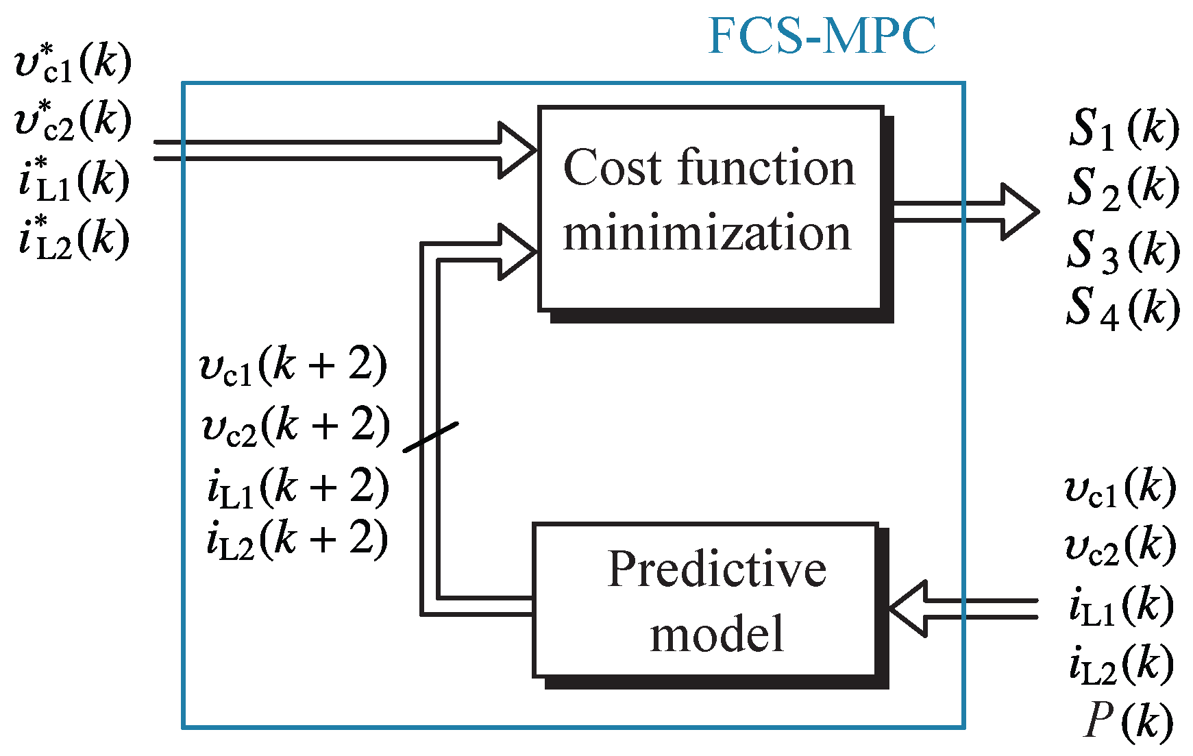
3.3.1. Finite Control Set–Model Predictive Control

One non-linear technique employed to control the DBI is based on the FCS–MPC algorithm. This strategy of control was proposed by the authors in [15]. Therefore, a summary of this strategy is presented below.
The general control diagram of the DBI is based on two cascaded control loops. The first control loop is composed by an MPPT method and a PI regulator for the input capacitor’s voltage, as explained in the previous sections. Then, the output of the input voltage controller is the active power reference, which is used in the next control loop. The FCS–MPC strategy is employed in the second control loop for the inductor’s current and output capacitor’s voltage, as shown in Figure 9. The details of this strategy can be found in [15].
In this work, the objectives of the cost function were slightly changed. The output current was not considered since the main approach is the individual control of each DC–DC converter. Therefore, the global structure of the cost function has two components:
G = λ 1 g 1 + λ 2 g 2
where:
g 1 = 1 i L 1 n 2 i L 1 * i L 1 p 2 + 1 i L 2 n 2 i L 2 * i L 2 p 2 g 2 = 1 υ c 1 n 2 υ c 1 * υ c 1 p 2 + 1 υ c 2 n 2 υ c 2 * υ c 2 p 2
g 1 is the quadratic error of the inductor currents; g 2 is the quadratic error of the capacitor voltages; λ 1 and λ 2 are the weight factors, which can determine the degree of relevance of each variable in the process. In this case, the main goal is the capacitor voltage and the second goal is the inductor current. Therefore, the weight factor λ 2 is higher than λ 1 . The weight factors were obtained by an empirical procedure, and the selected values were λ 1 = 1 and λ 2 = 75 .

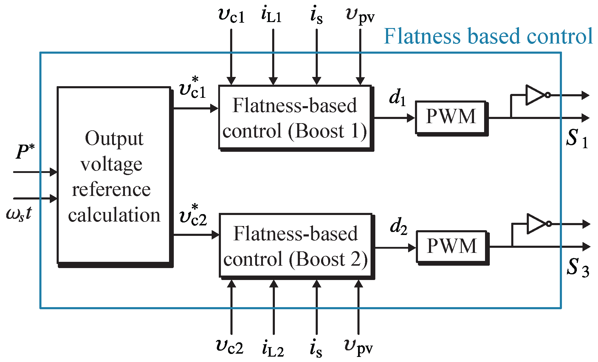
3.3.2. Flatness-Based Control

For the dual-boost inverter, the control strategy based on differential flatness theory was presented in [14]. A more detailed review of the main approaches can be found in [14,29,30].
This control strategy for the DBI considers an individual control for each boost converter. In such a scenario, the control scheme is composed by two cascaded control loops, as seen in Figure 10. As explained above, the PV voltage error is regulated using a PI controller whose output is the active power reference P * , which is employed to calculate the output voltage reference of each boost converter. The same analysis, presented in the linear control strategy to calculate the output voltage reference, was used in this case. The next control loop (inner control loop), based on flatness theory, regulates the output voltage of each boost converter, which is indirectly accomplished through the regulation of the energy stored in each output capacitor.
To analyze the flatness propriety of the DC–DC converter, the chosen candidate flat output, in this case, the stored energy through the converter [29,31], is written as
y 1 = 1 2 L 1 i L 1 2 + 1 2 C 1 υ c 1 2 = ϕ ( i L 1 , υ c 1 )
The flatness theory was verified through the following conditions:
i L 1 = φ i L 1 y 1 , y 1 ˙
υ c 1 = φ υ c 1 y 1 , y 1 ˙
d 1 = ψ 1 y 1 , y 1 ˙ , y 1 ¨
All variables can be expressed as a function of the flat output and its derivatives without solving any differential equations. Then, the system is flat, and it is possible to indirectly control all the variables through a control of y 1 .
To ensure reference tracking, a third-order control law was proposed:
k 1 y 1 * y 1 + k 2 y 1 * y 1 d t + k 3 y ˙ 1 * y 1 ˙ + k 4 y ¨ 1 * y 1 ¨ = 0
The constants k 1 , k 2 , k 3 , and k 4 are calculated as follows:
k 1 = 2 ξ ω n p + ω n 2 k 2 = p ω n 2 k 3 = 2 ξ ω n + p k 4 = 1
where ξ is the damping factor, ω n is the pulsation, and p is the value of one pole.

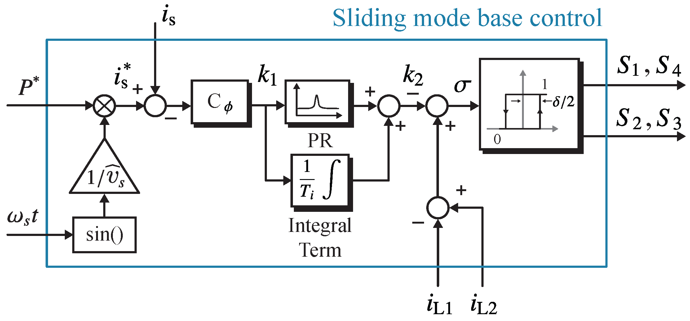
3.3.3. Sliding-Mode-Based Control

The control for the DBI based on the sliding mode approach was presented in [18], where the experimental results were obtained with a fixed source at the input. In this case, the global switching control strategy for the DBI was used and implemented. The same control approach was considered in this work with an extra control loop (PV voltage control loop). The control scheme shown in Figure 11 is composed of two cascaded current control loops and a PV voltage control loop.
The objective of the inner control loop is the current regulation of the boost converters. The difference between these currents is controlled through the sliding mode strategy, which is based on the equivalent control approach [17]. The selection of the switching surface is the most important aspect in the design of control, because it determines the behavior of the inverter. Then, the equivalent control was obtained to guarantee the feasibility of the sliding motion over the switching surface, and the existence condition was verified.
In this case, the difference between the current of the inductors can regulate indirectly the output voltage of the inverter [16]. Therefore, the sliding surface ( σ ( t ) ) was defined as shown in Equation (25).
σ ( t ) = k 2 ( t ) + i L 2 ( t ) i L 1 ( t )
where k 2 ( t ) is the output of external control loop.
On the other hand, the outer loop regulates the grid current of the DBI. Since the current reference is sinusoidal, a PR controller was used, which was tuned to the grid frequency ω s . The angle of i s * was obtained from a PLL, which was used to reconstruct a sinusoidal waveform enabling the synchronization with the grid [27,32]. The amplitude for the current reference was provided by the PI controller, which regulates the input capacitor’s ( C pv ) voltage.
Furthermore, a phase compensator C ϕ composed of a pole and a zero and an integral term were introduced in the control diagram to increase the phase margin and compensate the parameter differences between each DC–DC converter. A deeper analysis of this strategy can be found in [18].

4. Control Strategies Comparison

In order to achieve a comparison and validate the analysis of the four control strategies, the grid-connected dual-boost inverter with the PV panel as the input source was simulated in the PLECs software. The parameters of the PV panel and the inverter are presented in Table 3. Notice that the parameters of the inverter and the PV panel are the same for the four control strategies.

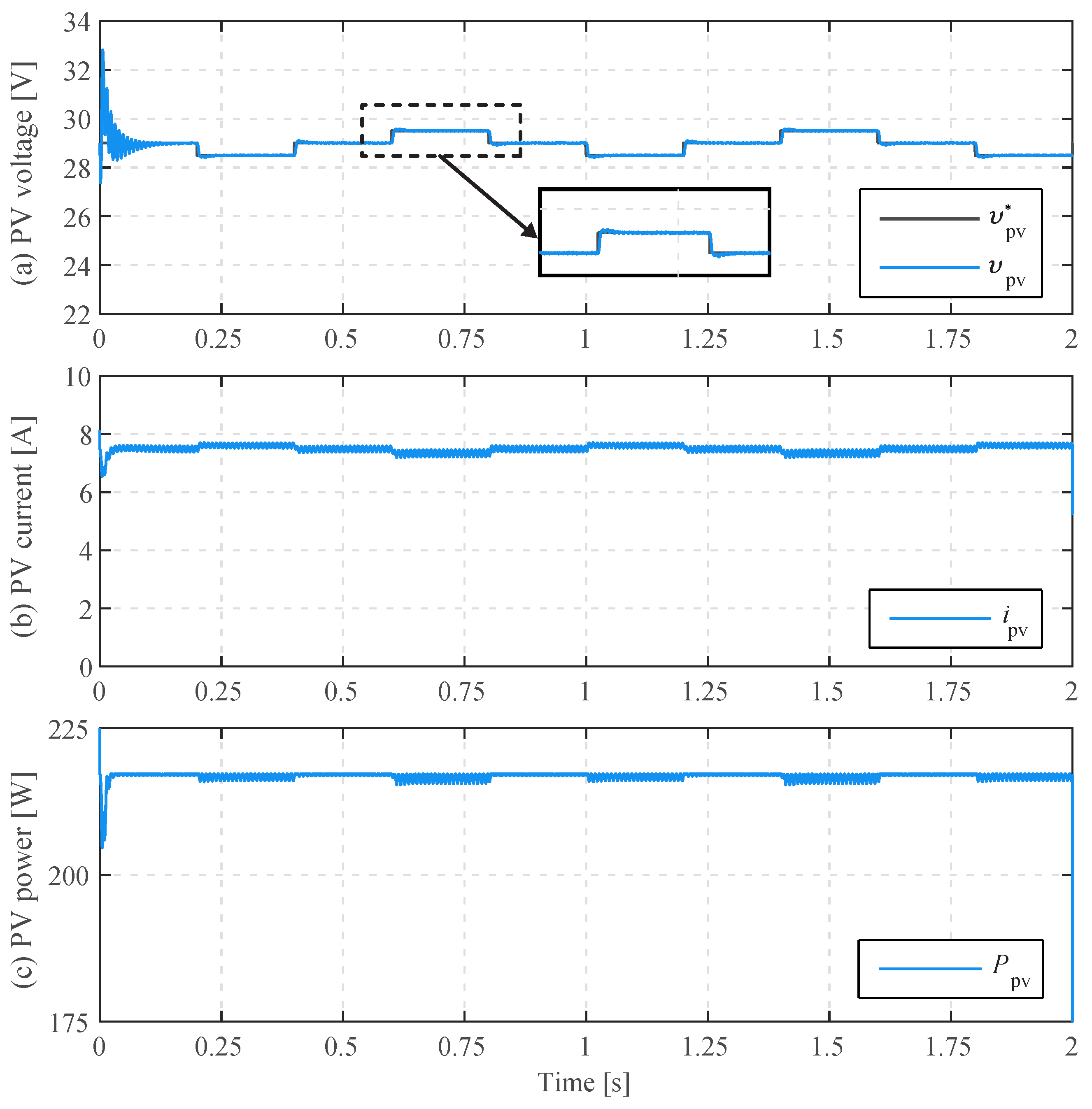
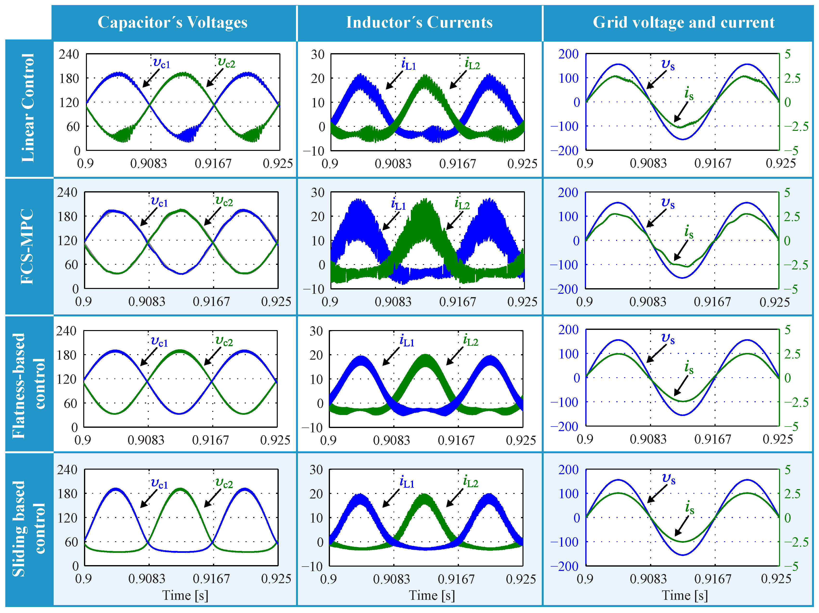
4.1. Steady-State Results

Figure 12 and Figure 13 present the simulation results for the DBI under steady-state behavior. These results were obtained in the nominal operation point, i.e., a solar irradiance of 1000 W/m 2 .
Figure 12 shows the behavior of the PV side for the linear control. The results of the PV side with the other control strategies are similar. For this reason, only the simulation results of the PV side with linear control are presented.
The reference of the PV voltage and its measurement are observed in Figure 12a, where the three voltage levels around the maximum power point can be identified when the PV panel is operating under constant solar irradiance. Furthermore, the PV current and power are presented in Figure 12b and Figure 12c, respectively. In these figures, the maximum PV module’s current and power can be identified.
The output capacitor’s voltages are composed by a DC-bias and an AC component, as shown in the first column of Figure 13. The AC component of the capacitor’s voltages with the linear control, FCS–MPC, and flatness-based strategies is purely sinusoidal, in which the maximum amplitude is around 77 V, and their phases are shifted 180 . The DC voltage component is 112.7 V, as expected. On the other hand, the DC component is 58 V with the sliding mode control, which is double the input voltage; this is an effect of the sliding mode strategy.
The second column of Figure 13 shows the behavior of the inductor’s current in each boost converter. The current waveforms are composed by a non-pure sinusoidal, where the maximum and minimum values are the same for both boost converters. Additionally, the phases are shifted 180 ; this is a similar effect to the one observed in the voltage. Moreover, the current through the inductors ( i L 1 and i L 2 ) in the four control selected reach a negative value, due to the circulating power. The current ripple chosen in the design was 5 A; this was achieved with the linear control, flatness-based control, and sliding mode control. However, the variable switching frequency inherent to FCS–MPC produces a higher current ripple. An alternative to solve this issue was proposed in [33], where the control of the switching period was introduced in the cost function.
The grid voltage and current are illustrated in the third column of Figure 13, where it is possible to identify that the current injected to the grid is sinusoidal and in phase with the grid voltage for the four control strategies.
To analyze the power quality of the DBI with the four control strategies, the grid current spectrum and its total harmonic distortion (THD) were obtained, as shown in Figure 14. Furthermore, the IEEE standard 1547 is introduced in these figures to identify the limits of each harmonic. As can be observed, the THD of the grid current fulfills the standard (THD < 5%) for the four cases. In the linear control, the odd harmonics (the third, fifth, and seventh) are strongly marked. Nevertheless, the THD of the grid current is 3.85%, which is within the accepted range by the standard. On the other hand, the THD of FCS–model predictive control is 3.58%. This is a very good result, considering that the waveform of the grid current has appreciable oscillations. In the flatness-based control, the third and fifth harmonics are predominant in the frequency spectrum. The total harmonic distortion is 2.59%. Finally, the frequency spectrum of the grid current obtained with the sliding mode control is shown in Figure 14d. Furthermore, the THD is added in this figure. As can be observed, the harmonics and THD are within the standard limits.

4.2. Comparison

The main parameters considered in the comparison are the number of cascaded control loops, total number of measured variables, and two performance metrics [34]: the total harmonic distortion (THD) and averaged switching frequency.
For the linear control, the control targets are the input capacitor’s voltage υ pv , the output capacitor’s voltages ( υ c 1 , υ c 2 ), and the inductor’s currents ( i L 1 , i L 2 ). In the case of FCS–MPC, the main control goals are the current through the inductor and voltage in the output capacitor for each boost converter. Therefore, a cascaded control loop scheme was used, where the first control loop regulates the voltage of the input capacitor C pv , followed by the FCS–MPC stage. The flatness-based control scheme consists of two cascaded loops. The targets of its first control loop are similar to the control scheme of the linear control, i.e., input capacitor’s voltage. The second loop control regulates the energy stored in the output capacitors C 1 , C 2 and inductors L 1 , L 2 of the DBI. These three control strategy are based on the individual switching strategy. In a different way, the control based on the sliding mode approach considers the output current of the DBI, as the main control purpose. To achieve this objective, a cascaded control scheme with three loops was employed. The target of the first loop, like the previous schemes, is the voltage of the input capacitor. The output current of the DBI is the control objective of the second control loop. To continue, the inner control loop determines the switching surface based on the difference of the current in the inductors regulation.
Considering the description of the control schemes mentioned before, five control loops in total are required to regulate the DBI with linear control. For FCS–MPC and flatness-based control, two and three control loops in total are necessary, respectively, while the sliding-mode-based control presents three control loops. On the other hand, the linear control, FCS–MPC, and flatness-based control strategies are based on the individual switching strategy. For this reason, the measured variables used in these control schemes are seven, which are the input current and voltage ( i pv , υ pv ), the inductor’s current ( i L 1 , i L 2 ), and the output capacitor’s voltage ( υ c 1 , υ c 2 ). Since the sliding mode control is based on a current regulation, fewer sensors are required. Hence, the output voltage is not directly controlled and does not need to be measured. Therefore, five variables are measured.
The averaged switching frequency ( f ¯ sw ) is another point to analyze, because this parameter is directly associated with the inductor’s current ripple. In the linear, flatness-based, and sliding mode controls, the average switching frequency obtained was around 80 kHz and the current ripple was around 5A. However, in FCS–MPC, the averaged switching frequency was 80 kHz, while the current ripple in the positive peak was 9.94 A. It is important to indicate that the current ripple does not correspond to the design, since the switching frequency in FCS–MPC is variable, and it is difficult to establish the current ripple for all ranges.
To evaluate the power quality obtained with each control strategy, the total harmonic distortion and spectrum of the grid current were analyzed. The spectrum of the grid current obtained with the four control methods complies with the IEEE standard 1547, as can be observed in Table 4. However, the highest THD among the four controls was obtained with the linear control strategy, because the output current of the DBI with the linear control contains more oscillations than with other control strategies.
Finally, a summary with the main features of each control strategy is presented in Table 4. The output current of the inverter with the four control strategies complies with the IEEE standard. However, the linear control presents the highest current’s THD, followed by FCS–MPC.
The linear control scheme has the highest number of the control loops to regulate the DBI. Moreover, the design and tuning of the parameters of the PR controllers are non-trivial procedures. On the other hand, FCS–MPC presents a variable switching frequency, requiring a redesign of the grid filter to achieve the desired current’s ripple. Furthermore, the tuning of the weight factor is a challenging task due to the different dynamics of the control objectives.
Although the switching frequency obtained with sliding mode control is variable, the THD of the grid current presents the best result. Furthermore, this control strategy is focused on the current regulation of the inverter, which means that fewer sensors are used, since the capacitor voltage υ c 1 , υ c 2 sensors are not required.
Considering all the comparison parameters mentioned above, the sliding mode control appears to be the most attractive control strategy for the DBI.

5. Conclusions

In this paper, four control strategies for the dual-boost inverter (DBI), a mainstream topology for single-stage PV microinverters, were reviewed and compared. In particular, the control strategies that were compared were classical linear control, FCS–MPC, flatness-based control, and sliding-mode-based control. Additionally, a detail review of the DBI model, the DBI’s switching strategies, and the global DBI’s control scheme were presented.
The comparison of the control strategies showed that the linear controller, FCS–MPC, and flatness-based control require the largest amount of sensors (7), while sliding mode control requires only five sensors.
On the other hand, the linear control presented the lowest averaged switching frequency (79,060 Hz) when compared to FCS–MPC (79,140 Hz), flatness-based control (79,980 Hz), and sliding mode control (85,680 Hz).
Regarding the inductor’s current ripple in each boost converter, sliding mode control showed the lowest value (5.10 A), closely followed by linear control (5.2 A) and flatness-based control (5.23 A). However, the inductor’s current ripple in FCS–MPC (9.94 A) was almost twice that of sliding mode control. Thus, FCS–MPC resulted in being the worst alternative in terms of a possible ripple-related failure of the capacitors.
Finally, the main goal of this power converter is to generate a sinusoidal wave form. The harmonic contents of the grid currents, obtained from applying the control strategies, were contrasted with the IEEE Std. 1547, and the result showed that all the control strategies complied with the standard. Additionally, the analysis of the grid current’s harmonic content showed that the best-performing control strategy was sliding mode control with a current THD of 2.48%, while the other control strategies (linear control 3.85%, FCS–MPC 3.58%, and flatness-based control 2.59%) showed the lowest performance.
In conclusion, sliding-mode-based control presented the best trade-off between its advantages and disadvantages; therefore, it was selected as the most promising control strategy for the DBI in single-stage PV microinverter applications.

Author Contributions

Conceptualization, D.L.-C., H.R. and S.K.; methodology, H.R. and S.K.; validation, D.L.-C. and H.R.; formal analysis, D.L.-C., H.R. and N.M.; investigation, D.L.-C.; resources, S.K. and F.F.-B.; writing—original draft preparation, D.L.-C.; writing—review and editing, H.R., N.M. and F.F.-B.; supervision, S.K. and J.R.; funding acquisition, S.K. All authors have read and agreed to the published version of the manuscript.

Funding

This research received no external funding.

Institutional Review Board Statement

Not applicable.

Informed Consent Statement

Not applicable.

Data Availability Statement

Not applicable.

Acknowledgments

The authors acknowledge the financial support provided by AC3E (ANID/ BASAL/FB0008), SERC Chile (ANID/FONDAP/15110019), and the Innovative Energy Technologies Center at the Universidad Austral de Chile, INVENT UACh.

Conflicts of Interest

The authors declare no conflict of interest.

References

  1. Research and Markets. Global Solar Microinverter Market. 2021. Available online: https://www.researchandmarkets.com/reports/5235685/global-solar-microinverter-market-by-type (accessed on 15 March 2022).
  2. Jain, S.; Agarwal, V. A Single-Stage Grid Connected Inverter Topology for Solar PV Systems With Maximum Power Point Tracking. IEEE Trans. Power Electron. 2007, 22, 1928–1940. [Google Scholar] [CrossRef] [Green Version]
  3. Li, Q.; Wolfs, P. A Review of the Single Phase Photovoltaic Module Integrated Converter Topologies With Three Different DC Link Configurations. IEEE Trans. Power Electron. 2008, 23, 1320–1333. [Google Scholar] [CrossRef] [Green Version]
  4. Meneses, D.; Blaabjerg, F.; Garcia, O.; Cobos, J.A. Review and Comparison of Step-Up Transformerless Topologies for Photovoltaic AC-Module Application. IEEE Trans. Power Electron. 2013, 28, 2649–2663. [Google Scholar] [CrossRef] [Green Version]
  5. Alluhaybi, K.; Batarseh, I.; Hu, H. Comprehensive Review and Comparison of Single-Phase Grid-Tied Photovoltaic Microinverters. IEEE J. Emerg. Sel. Top. Power Electron. 2020, 8, 1310–1329. [Google Scholar] [CrossRef]
  6. Caceres, R.; Barbi, I. A boost DC-AC converter: Operation, analysis, control and experimentation. In Proceedings of the IECON ’95-21st Annual Conference on IEEE Industrial Electronics, Orlando, FL, USA, 6–10 November 1995; Volume 1, pp. 546–551. [Google Scholar] [CrossRef]
  7. Sanchis, P.; Ursaea, A.; Gubia, E.; Marroyo, L. Boost DC-AC inverter: A new control strategy. IEEE Trans. Power Electron. 2005, 20, 343–353. [Google Scholar] [CrossRef]
  8. Jang, M.; Agelidis, V.G. A Minimum Power-Processing-Stage Fuel-Cell Energy System Based on a Boost-Inverter With a Bidirectional Backup Battery Storage. IEEE Trans. Power Electron. 2011, 26, 1568–1577. [Google Scholar] [CrossRef]
  9. Zhu, G.; Tan, S.; Chen, Y.; Tse, C.K. Mitigation of Low-Frequency Current Ripple in Fuel-Cell Inverter Systems Through Waveform Control. IEEE Trans. Power Electron. 2013, 28, 779–792. [Google Scholar] [CrossRef] [Green Version]
  10. Jang, M.; Ciobotaru, M.; Agelidis, V.G. A Single-Phase Grid-Connected Fuel Cell System Based on a Boost-Inverter. IEEE Trans. Power Electron. 2013, 28, 279–288. [Google Scholar] [CrossRef]
  11. Abeywardana, D.B.W.; Hredzak, B.; Agelidis, V.G. A Rule-Based Controller to Mitigate DC-Side Second-Order Harmonic Current in a Single-Phase Boost Inverter. IEEE Trans. Power Electron. 2016, 31, 1665–1679. [Google Scholar] [CrossRef]
  12. Caceres, R.O.; Barbi, I. A boost DC-AC converter: Analysis, design, and experimentation. IEEE Trans. Power Electron. 1999, 14, 134–141. [Google Scholar] [CrossRef]
  13. Jha, K.; Mishra, S.; Joshi, A. High-Quality Sine Wave Generation Using a Differential Boost Inverter at Higher Operating Frequency. IEEE Trans. Ind. Appl. 2015, 51, 373–384. [Google Scholar] [CrossRef]
  14. Renaudineau, H.; Lopez, D.; Flores-Bahamonde, F.; Kouro, S. Flatness-based control of a boost inverter for PV microinverter application. In Proceedings of the 2017 IEEE 8th International Symposium on Power Electronics for Distributed Generation Systems (PEDG), Florianopolis, Brazil, 17–20 April 2017; pp. 1–6. [Google Scholar] [CrossRef]
  15. Lopez, D.; Flores-Bahamonde, F.; Kouro, S.; Perez, M.A.; Llor, A.; Martínez-Salamero, L. Predictive control of a single-stage boost DC-AC photovoltaic microinverter. In Proceedings of the IECON 2016-42nd Annual Conference of the IEEE Industrial Electronics Society, Florence, Italy, 23–26 October 2016; pp. 6746–6751. [Google Scholar] [CrossRef]
  16. Cortes, D.; Vazquez, N.; Alvarez-Gallegos, J. Dynamical Sliding-Mode Control of the Boost Inverter. IEEE Trans. Ind. Electron. 2009, 56, 3467–3476. [Google Scholar] [CrossRef]
  17. Flores-Bahamonde, F.; Valderrama-Blavi, H.; Bosque-Moncusi, J.M.; García, G.; Martínez-Salamero, L. Using the sliding-mode control approach for analysis and design of the boost inverter. IET Power Electron. 2016, 9, 1625–1634. [Google Scholar] [CrossRef]
  18. Lopez-Caiza, D.; Flores-Bahamonde, F.; Kouro, S.; Santana, V.; Müller, N.; Chub, A. Sliding Mode Based Control of Dual Boost Inverter for Grid Connection. Energies 2019, 12, 4241. [Google Scholar] [CrossRef] [Green Version]
  19. El Aroudi, A.; Haroun, R.; Al-Numay, M.; Huang, M. Multiple-Loop Control Design for a Single-Stage PV-Fed Grid-Tied Differential Boost Inverter. Appl. Sci. 2020, 10, 4808. [Google Scholar] [CrossRef]
  20. Abeywardana, D.B.W.; Hredzak, B.; Agelidis, V.G. An Input Current Feedback Method to Mitigate the DC-Side Low-Frequency Ripple Current in a Single-Phase Boost Inverter. IEEE Trans. Power Electron. 2016, 31, 4594–4603. [Google Scholar] [CrossRef]
  21. Huang, S.; Tang, F.; Xin, Z.; Xiao, Q.; Loh, P.C. Grid-Current Control of a Differential Boost Inverter With Hidden LCL Filters. IEEE Trans. Power Electron. 2019, 34, 889–903. [Google Scholar] [CrossRef]
  22. Chen, W.L.; Yang, C.H.; Lin, C.T.; Xu, M.S.; Chen, K.F. Voltage Modulation and Current Control of Boost Inverters for Stand-Alone or Grid-Tied Operation. IEEE Trans. Power Electron. 2020, 35, 8726–8736. [Google Scholar] [CrossRef]
  23. Sanchis Gurpide, P.; Alonso Sadaba, O.; Marroyo Palomo, L.; Meynard, T.; Lefeuvre, E. A new control strategy for the boost DC-AC inverter. In Proceedings of the 2001 IEEE 32nd Annual Power Electronics Specialists Conference (IEEE Cat. No.01CH37230), Vancouver, BC, Canada, 17–21 June 2001; Volume 2, pp. 974–979. [Google Scholar]
  24. Kouro, S.; Perez, M.A.; Rodriguez, J.; Llor, A.M.; Young, H.A. Model Predictive Control: MPC’s Role in the Evolution of Power Electronics. IEEE Ind. Electron. Mag. 2015, 9, 8–21. [Google Scholar] [CrossRef]
  25. Kouro, S.; Wu, B.; Abu-Rub, H.; Blaabjerg, F. Photovoltaic energy conversion systems. In Power Electronics for Renewable Energy Systems, Transportation and Industrial Applications; John Wiley & Sons: Hoboken, NJ, USA, 2014; pp. 160–198. [Google Scholar]
  26. Wang, L. PID Control System Design and Automatic Tuning Using MATLAB/Simulink; John Wiley & Sons: Hoboken, NJ, USA, 2020. [Google Scholar]
  27. Teodorescu, R.; Liserre, M.; Rodriguez, P. Grid Converters for Photovoltaic and Wind Power Systems; John Wiley & Sons: Hoboken, NJ, USA, 2011; p. 29. [Google Scholar]
  28. Bouneb, B.; Grant, D.M.; Cruden, A.; McDonald, J.R. Grid connected inverter suitable for economic residential fuel cell operation. In Proceedings of the 2005 European Conference on Power Electronics and Applications, Dresden, Germany, 11–14 September 2005; p. 10. [Google Scholar]
  29. Renaudineau, H. Hybrid Renewable Energy Sourced System: Energy Management & Self-Diagnosis. Ph.D. Thesis, Université de Lorraine, Nancy, France, 2013. [Google Scholar]
  30. Soheil-Hamedani, M.; Zandi, M.; Gavagsaz-Ghoachani, R.; Nahid-Mobarakeh, B.; Pierfederici, S. Flatness-based control method: A review of its applications to power systems. In Proceedings of the 2016 7th Power Electronics and Drive Systems Technologies Conference (PEDSTC), Tehran, Iran, 16–18 February 2016; pp. 547–552. [Google Scholar] [CrossRef]
  31. Gensior, A.; Woywode, O.; Rudolph, J.; Guldner, H. On Differential Flatness, Trajectory Planning, Observers, and Stabilization for DC–DC Converters. IEEE Trans. Circuits Syst. I Regul. Pap. 2006, 53, 2000–2010. [Google Scholar] [CrossRef]
  32. Rodríguez, P.; Luna, A.; Muñoz-Aguilar, R.S.; Etxeberria-Otadui, I.; Teodorescu, R.; Blaabjerg, F. A Stationary Reference Frame Grid Synchronization System for Three-Phase Grid-Connected Power Converters Under Adverse Grid Conditions. IEEE Trans. Power Electron. 2012, 27, 99–112. [Google Scholar] [CrossRef]
  33. Aguirre, M.; Kouro, S.; Rojas, C.A.; Rodriguez, J.; Leon, J.I. Switching Frequency Regulation for FCS–MPC Based on a Period Control Approach. IEEE Trans. Ind. Electron. 2018, 65, 5764–5773. [Google Scholar] [CrossRef]
  34. Karamanakos, P.; Geyer, T. Guidelines for the Design of Finite Control Set Model Predictive Controllers. IEEE Trans. Power Electron. 2020, 35, 7434–7450. [Google Scholar] [CrossRef]
Figure 1. Differential mode inverter scheme and principle of operation.
Applsci 12 05952 g001
Figure 2. Control objectives for DBI: (a) Individual boost converter switching strategy. (b) Global switching strategy.
Applsci 12 05952 g002
Figure 3. Dual-boost inverter topology.
Applsci 12 05952 g003
Figure 4. Equivalent model of the DBI with grid connection.
Applsci 12 05952 g004
Figure 5. Global control strategies for DBI.
Applsci 12 05952 g005
Figure 6. Linear control scheme of the grid-connected DBI.
Applsci 12 05952 g006
Figure 7. (a) Equivalent model of the DBI without resistance. (b) Phasor diagram.
Applsci 12 05952 g007
Figure 8. (a) Current control loop of the linear control. (b) Voltage control loop of the linear control.
Applsci 12 05952 g008
Figure 9. The control scheme of the FCS–MPC for the grid-connected DBI.
Applsci 12 05952 g009
Figure 10. Control scheme of the flatness-based control for DBI.
Applsci 12 05952 g010
Figure 11. The cascaded control scheme of the grid-connected DBI, with external PR controller and internal sliding mode controller.
Applsci 12 05952 g011
Figure 12. Simulation results of the PV side with the linear control for DBI: (a) PV voltage. (b) PV current. (c) PV power.
Applsci 12 05952 g012
Figure 13. Summary the simulation results at the nominal operation point of the control strategies for DBI.
Applsci 12 05952 g013
Figure 14. Grid current spectrum of DBI at nominal power with: (a) Linear control. (b) FCS–model predictive control. (c) Flatness-based control. (d) Sliding mode control.
Applsci 12 05952 g014
Table 1. Review of the control strategies for the dual-boost inverter.
Type of LoadControl StrategyControl Objectives—SurfaceRef.
1st familyR and non-linear loadLinear control (PIs)Capacitor voltage and inductor current [7,8]
R and RCLinear control (PIs)Capacitor voltage and inductor current [9]
Grid-connectionLinear control (PRs)Capacitor voltage and inductor current [10]
Grid-connectionLinear control (PR+PI)Capacitor voltage and inductor current [11]
R, L, and non-linear loadSliding mode control σ = k 1 ( i L 1 i L 1 * ) + k 2 ( υ c 1 υ c 1 * ) k [12]
ResistanceDynamic linearizing modulatorCapacitor voltage [13]
Grid-connectionFlatness-based controlEnergy stored in capacitors and inductors [14]
Grid-connectionFinite control set—MPCCapacitor voltage and inductor current [15]
2nd familyR and non-linearSliding mode control σ = i L 1 i L 2 k [16]
ResistanceSliding mode control σ = i L 1 i L 2 k [17]
Grid-connectionSliding mode control σ = i L 1 i L 2 k [18,19]
Table 2. Dual-boost inverter switching and conduction states.
Switching State S 1 S 2 S 3 S 4 Conduction StateOutput CurrentInductor Currents
101101 i s > 0 i L 1 < 0 , i L 2 > 0
2 i s < 0
201013 i s > 0 i L 1 < 0 , i L 2 < 0
4 i s < 0
310105 i s > 0 i L 1 > 0 , i L 2 > 0
6 i s < 0
410017 i s > 0 i L 1 > 0 , i L 2 < 0
8 i s < 0
Table 3. Simulation parameters of the DBI.
SymbolParameterValue
PV Parameters
V m p p PV voltage at MPP29 V
P p v PV power216 W
C p v Input capacitor25 mF
Grid Parameters
υ s Grid voltage110 V rms
f s Grid frequency60 Hz
L s Grid filter inductance10 mH
Converter Parameters
L 1 , L 2 Boost converters’ inductors55 μ H
C 1 , C 2 Boost converters’ capacitors5 μ F
Table 4. Main parameters of comparison.
ParametersLinear ControlFCS–MPCFlatness-Based ControlSliding Mode Control
Total number of control loops5233
Total number of measured variables7775
Averaged switching frequency79,060 Hz79,140 Hz79,980 Hz85,680 Hz
Ripple of inductor currents5.2 A9.94 A5.23 A5.10 A
THD i s 3.85%3.58%2.59%2.48%
Publisher’s Note: MDPI stays neutral with regard to jurisdictional claims in published maps and institutional affiliations.

