Article

Measurement of Sub-Surface Microstructures Based on a Developed Ultrasonic Atomic Force Microscopy

State Key Lab of Fluid Power and Mechatronic Systems, School of Mechanical Engineering, Zhejiang University, Hangzhou 310027, China
*
Author to whom correspondence should be addressed.
Appl. Sci. 2022, 12(11), 5460; https://doi.org/10.3390/app12115460
Submission received: 11 May 2022 / Revised: 25 May 2022 / Accepted: 25 May 2022 / Published: 27 May 2022

Abstract

:
Accurate and non-destructive technology for detection of subsurface defect has become a key requirement with the emergence of various ultra-precision machining technologies and the application of ultra-precision components. The combination of acoustic technique for sub-surface detection and atomic force microscopy (AFM) for measurement with high resolution is a potential method for studying the subsurface structure of workpiece. For this purpose, contact-resonance AFM (CR-AFM) is a typical technique. In this paper, a CR-AFM system with a different principle from commercially available instruments is set up and used for the detection of sub-surface Si samples with grating structures and covered by different thickness of highly oriented pyrolytic graphite (HOPG). The influence of subsurface burial depth on the detection capability is studied by simulations and experiments. The thickest HOPG film allowing for sub-surface measurement by the proposed method is verified to be about 30 μm, which is much larger than the feature size of the subsurface microstructure. The manuscript introduces the difference between this subsurface topography measurement principle and the commercially available AFM measurement principle, and analyzes its advantages and disadvantages. The experimental results demonstrates that the technique has the capability to reveal sub-surface microstructures with relatively large buried depth and is potential for engineering application in ultra-precision technologies.

1. Introduction

With the continuous progress of ultraprecision machining technology, various ultra-precision components are widely used in aerospace, quantum communications, new energy, biomedical and other important fields related to the national economy and people’s livelihood [1,2]. In addition to the stringent requirements for machining accuracy, surface/subsurface integrity and service reliability are also required by ultra-precision components. The surface and subsurface defects of ultra-precision components are key factors affecting their service reliability [3]. Thus, high-precision measurement of surface and sub-surface defects of ultra-precision components is not only a key requirement for ensuring the quality of ultra-precision processing, but also a frontier direction in the field of micro- and nanometrology.
Studies have shown that besides the inherent defects of the material itself, the complex mechanical, physical, and chemical interaction process between the tool and the material during the ultra-precision machining process are the main reasons for inducing defects of the machined parts [4]. The defect areas caused by the machining process mainly exist on the surface and subsurface of the workpiece [5]. Among them, surface defects are easy to detect by many existing measurement technologies and can also be removed by subsequent processes such as ultra-precision polishing. However, sub-surface defects are hidden under the surface layer and thus difficult to be detected and removed, which is a key factor affecting the performance and reliability of ultra-precision components [6,7]. Considering the scale of subsurface defect could be down to micrometric or even nanometric orders, traditional inspection technologies are facing severe technical challenges. It is important to develop new measurement methods suitable for high-resolution measurement and characterization of subsurface micro/nano-scale defects, so as to qualify the ultra-precision processing and reliability of ultra-precision processing components [4,8,9].
Many studies have shown that ultrasonic detection method is able to use the interactions between a focused ultrasound wave and materials to measure subsurface defects by analyzing the ultrasonic echo signals [9,10,11]. The ultrasonic detection has the advantages of wide materials applicability. However, the resolution of ultrasonic detection can only reach a few tens of microns, and it is quite challenging to measure micro/nano-scale subsurface defects due to the inevitable effect of diffraction limit in ultrasonic wave. On the other hand, atomic force microscopy (AFM) [12] can be completely free of the influence of diffraction limit, and has the advantage of achieving high resolution in the nanometric and even sub-nanometer scale [13]. However, considering that the interface between the AFM probe and the sample occurs only on the surface layer, conventional AFM can only be used for surface topography measurement and does not have the capability to obtain the information of subsurface structures [14].
Therefore, the advantage of subsurface detection capability of ultrasonic inspection and the advantage of high resolution measurement of AFM technique were considered to form the ultrasonic AFM technique. In recent days, some studies on combining AFM with ultrasonic excitation have been demonstrated and practiced to detect microstructures with tens or even hundreds of nanometers below the material surface. Perrin et al. [15] reconstructed the PDMS thin film materials embedded with silicon nanowires based on the dynamic model of the probe-sample coupling system by applying ultrasonic multi-frequency excitation to the AFM probe. Zhang W et al. [16] carried out related research work on acoustic scanning probe measurement technology of the sample mechanism. They obtained information on the nanostructure of HOPG 200 nm below the surface by means of high harmonic acoustic field excitation of the AFM. These tasks apply additional ultrasonic excitation to the tip or the sample of the AFM system and reveal the sub-surface image of the sample. However, the measurement capability for the buried depth of the subsurface microstructures in these experimental samples is less than 500 nm [17,18]. In addition to studying subsurface defects in samples, the CR-AFM technique can also be applied to study physical properties, such as stiffness, of various polymers or to examine the preparation quality of composite materials [19]. Wagner R et al. [20] measured and mapped the transverse elastic modulus of three types of cellulosic nanoparticles: tunicate cellulose nanocrystals, wood cellulose nanocrystals, and wood cellulose nanofibrils by CR-AFM. Cadena MJ et al. [21] obtained subsurface images from the same area of a polymer composite film containing single-walled carbon nanotube networks embedded in a polyimide matrix to estimate the depth of the buried carbon nanotube bundles by CR-AFM. It is desired to increase the buried depths of the detectable subsurface microstructures so that the measurement techniques can be applicable to more ultra-precision components.
In this paper, to explore whether the ultrasonic AFM has the ability to detect deeper subsurface defects with a larger buried depth up to micrometric level, a new prototype of ultrasonic AFM is built. A new contact resonance method is employed to enlarge the detectable buried depth by the ultrasonic AFM and the change of the contact resonance frequency is taken as the feedback signal. Different silicon gratings covered by HOPG films with thicknesses ranging from 400 nm to 35 μm are measured by the proposed method. Experiments show that the grating topography covered under the HOPG film can be clearly detected with a large buried depth up to 34.469 μm, which greatly improves the detection range of the existing UAFM for measurement of subsurface topography with large buried depths.

2. Materials and Methods

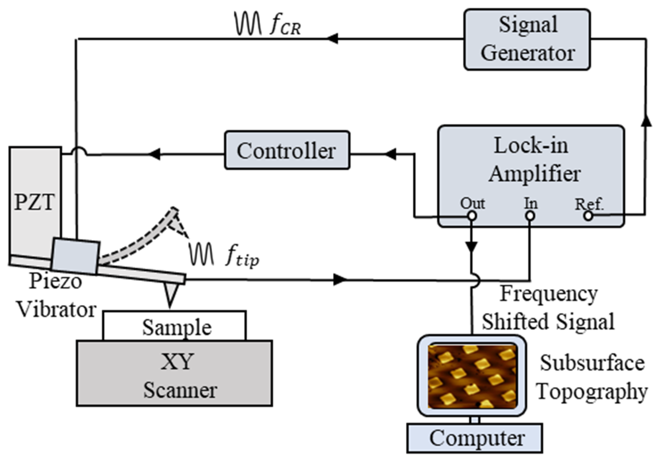
2.1. Contact-Resonance AFM

Figure 1 shows a schematic of the developed contact-resonance AFM (CR-AFM) for subsurface profile measurement. It is operated to obtain the information of subsurface microstructure via a probe applied with ultrasonic excitation where the frequency is near the contact resonance frequency of the probe and the sample. In this system, for the sake of easy operation and application, a piezoresistive cantilever probe is used in the system instead of traditional cantilever probe requiring a laser detection unit. The vibration signal of the piezoresistive probe is controlled by a lock-in amplifier in the process of probe scanning over the measured surface. During the scanning procedure, the vibration amplitude or frequency change of the probe is used as the feedback control signal to control the piezoelectric actuator carrying the probe up and down afterwards corresponding to the feedback signal. Since the subsurface microstructures would generate variation of the contact resonant frequency on the surface of the sample and thus change the tracking path of the probe controlled by the feedback control, the scanning image of the sub-surface structure can be obtained.
In the existing CR-AFM-based subsurface topography studies [22,23], the probe is given a constant external excitation signal for vibration and the contact force between the probe and the sample is adopted as the feedback signal and maintained constant during the scanning process. The frequency for the external excitation signal is the contact resonance frequency of the probe-sample system. In the scanning, if the sample has subsurface microstructures, it would lead to the change of the probe vibration amplitude, so that the amplitude signal of the probe vibration during the whole scanning process can be drawn to obtain the topography of the subsurface microstructure. The study in this paper adopts a new method based on CR-AFM. The main difference is that in this study, the contact resonance frequency of the probe-sample system is set as the feedback signal instead of the contact force in traditional method. During the scanning, the actual contact resonance frequency of each scanned point is detected in real time and the difference of the detected frequency from the reference frequency is used as the driving signal to the piezoelectric ceramic scanner. Since the subsurface microstructure will influence the resonance frequency of the probe-same system, the signals drawn by the piezoelectric ceramic scanner servo displacement during the scanning process could represent the subsurface topography of the sample. The advantage of using the resonance frequency over the conventionally used contact force as the feedback signal comes from the ability to acquire information from deeper subsurface structures. When using contact force as the feedback signal, the amplitude of the probe vibration differs along the scan path: the amplitude may be drastically suppressed when the probe vibration is at the off-resonant mode, resulting in a reduction of the energy transmitted from the probe into the sample and thus making it difficult to reach deeper subsurface structures. In our method, on the other hand, the energy of the vibration holds still at its maximum value for each measurement point, yielding a much better penetration capability.
The subsequent simulations and experiments will mainly discuss the proposed method, the detection capability of the method for subsurface topography at different burial depths will be studied, and the advantage with the traditional CR-AFM method will be compared.

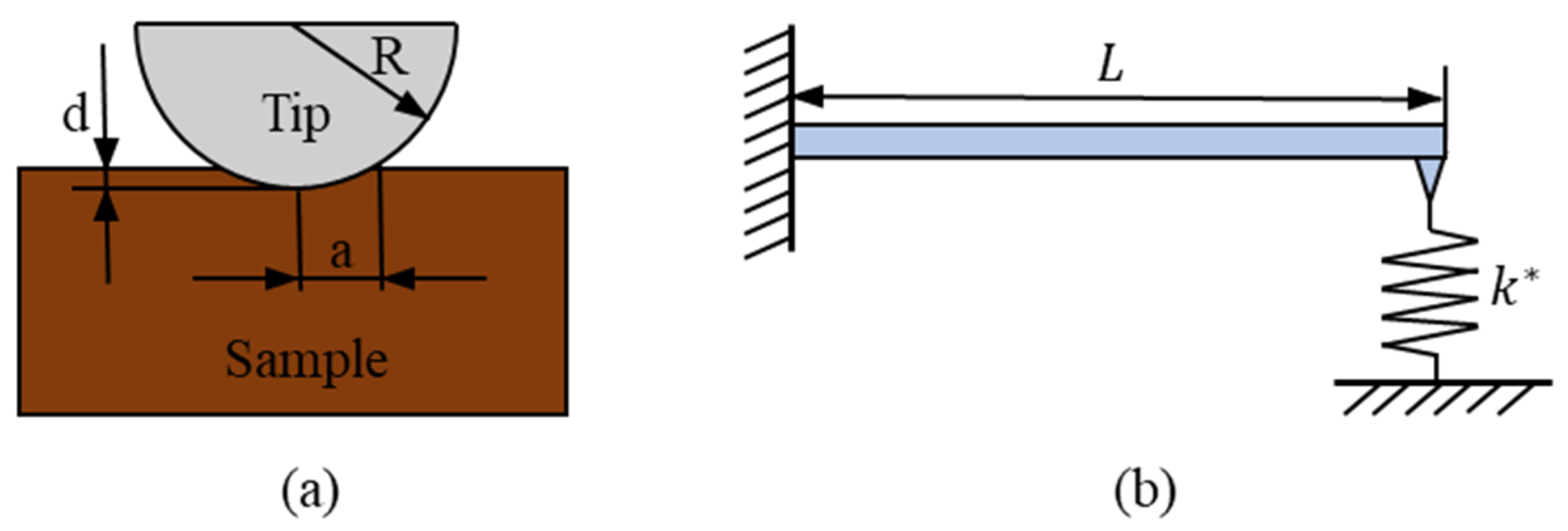
2.2. Theoretical Model

In this study, variations in subsurface morphology would directly change the contact stiffness at each scan point and lead to changes in the probe-sample contact resonance frequency. As described above, the change of contact resonance frequency of the probe-sample system is the focus of our research. The relevant equations are organized and derived in this part to demonstrate the effect of the change in contact stiffness on the resonant frequency of the probe-sample contact. The main physical model used in this study is shown in Figure 2.
A simplified model diagram of the contact between the tip of the probe and the sample surface is shown in Figure 2a. Note that the wavelength of ultrasonic excitation signal   λ is much larger than the contact radius a at the ultrasonic frequency, the contact process between the probe tip and the sample surface can be studied as a quasi-static physical process. Thus, the contact between the spherical tip and the sample surface can be explained by Hertz contact theory [24,25,26] as:
a = 3 F R 4 E * 3
d = 9 F 2 16 R E * 2 3
k * = 2 a E * = 6 E * 2 F R 3
E * = ( 1 γ s 2 ) E s + ( 1 γ t 2 ) E t
where F is the contact force between tip and sample, R is the tip radius, k * is the equivalent contact stiffness between probe tip and sample, E * is the equivalent elastic modulus between probe tip and sample, d is the pressing depth of probe, which is equal to the sum of tip and sample surface deformation, γ s and γ t represent the Poisson’s ratio of sample and tip, respectively, and E s and E t represent the elastic modulus of sample and tip, respectively.
Equation (4) reveals the influencing factors of the equivalent contact stiffness between the probe and the sample. When there are microstructures (such as pores, heterogeneous particles, etc.) exit on the subsurface of the sample, the elastic modulus and Poisson’s ratio of the sample will change, resulting in a change in the equivalent contact stiffness between the probe and the sample.
Since AFM cannot directly measure the elastic modulus of the material, but can extract the probe’s oscillation signal information during the scanning process, the change of the equivalent elastic modulus can be converted into a detectable probe vibration frequency change signal. The subsurface topography is characterized by the change of the contact resonance frequency of the probe. The simplified probe vibration model is shown in Figure 2b.
When the equivalent contact stiffness k * of the probe-sample system is equal to zero, the model is reduced to a simple free vibration model with a fixed end of a cantilever beam, and the partial differential Equation of its free vibration is written as:
E I δ 4 y δ x 4 + ρ A δ 4 y δ t 4 = 0
where E is the elastic modulus of cantilever, I presents the area moment of inertia of cantilever beam, which is equal to tb 3 /12 when we suppose that the cantilever beam has length L , density ρ , cross-sectional area A , cross-sectional area width t , and thickness b . The boundary conditions of Equation (5) are:
x = 0 :   y ( x ) = 0 ,   δ y ( x ) δ x = 0
  x = L :   δ 2 y ( x ) δ x 2 = 0 ,   δ 3 y ( x ) δ x 3 = 0
Thus, the characteristic equation of Equation (5) can be calculated as:
c o s k n L c o s h   k n L + 1 = 0
where n represents modal order of the vibration, k stands for wave number of cantilever oscillation, and k n L is the normalized modulus of infinite bending vibration modes of the cantilever.
When the equivalent contact stiffness k * of the probe-sample system is larger than zero, it means that the probe makes contact with the sample surface and exerts a force. At this point, the partial differential Equation for the vibration of the cantilever beam can still be expressed by Equation (5). However, under the influence of the contact force that is simplified to a spring, the boundary condition of Equation (5) becomes:
x = 0 :   y ( x ) = 0 ,   δ y ( x ) δ x = 0
  x = L :   δ 2 y ( x ) δ x 2 = 0 , E I δ 3 y ( x ) δ x 3 = k * y
after taking into account the new boundary conditions, the characteristic equation of the simplified model for contact stiffness k * can be obtained:
k k * ( k n L ) 3 ( 1 + c o s   k n L c o s h k n L ) = 3 ( s i n k n L c o s h k n L s i n h k n L c o s k n L )
where k * can be get from Equation (3) and k represents the spring stiffness of the cantilever beam.
The relationship between k n and f n is:
k n f n = 4 π 2 12 ρ b 2 E *
Then, for rectangular cantilever beams, the frequencies of vibration modes of the cantilever of the probe f n can be expressed as:
f n = 1 2 π E * I ρ A k n 2 ( k n L ) 2 2 π b L 2 E * 12 ρ
Equations (4) and (13) successfully relate the probe-sample equivalent contact stiffness in Equation (4) with the probe contact resonance frequency. Thus, the subsurface topography can be obtained by studying the variation of the resonant frequency of the probe contact during the scanning process. The CR-AFM system realizes the detection of subsurface defects according to this principle, that is, when the subsurface of the sample has microstructures such as particles, cracks, and holes, the contact stiffness of the sample surface would change, which correspondingly cause the change of the contact resonance of the probe. Thus, the above physical model is applied to the subsequent study.

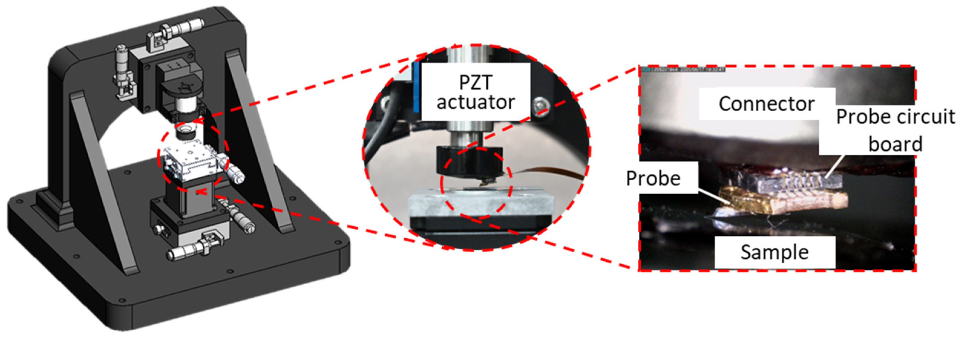
2.3. Equipment and Sample

A new prototype CR-AFM equipment built according to the schematic of Figure 1 is shown in Figure 3. It can be seen from the enlarged view that a piezoresistive cantilever probe (PRSA-L400-F30-Si-PCB, SCL-SENSOR) is attached to the piezoelectric actuator through a connector. The piezoelectric actuator has a stroke of 30 μm and a positioning resolution of 0.6 nm. Then, the contact resonant frequency of the probe and the sample is found by contacting the probe with the sample and sweeping the frequency, then an ultrasonic excitation near this frequency is applied to the probe cantilever by a peripheral signal generator. The property parameters of the cantilever probe are shown in Table 1.
The preparation process of the samples with subsurface microstructure for experiments is as follows. First, a grating with a width of 2 μm, a depth of 500 nm and a period of 4 μm is etched on a silicon wafer. The HOPG film is then transferred to the photolithographic silicon wafer by mechanical stripping, and under the action of van der Waals force, HOPG can be well combined with the surface of the silicon wafer [27,28]. Finally, AFM and white light interferometer are used to detect the thickness of the pasted HOPG film.

3. Results and Discussion

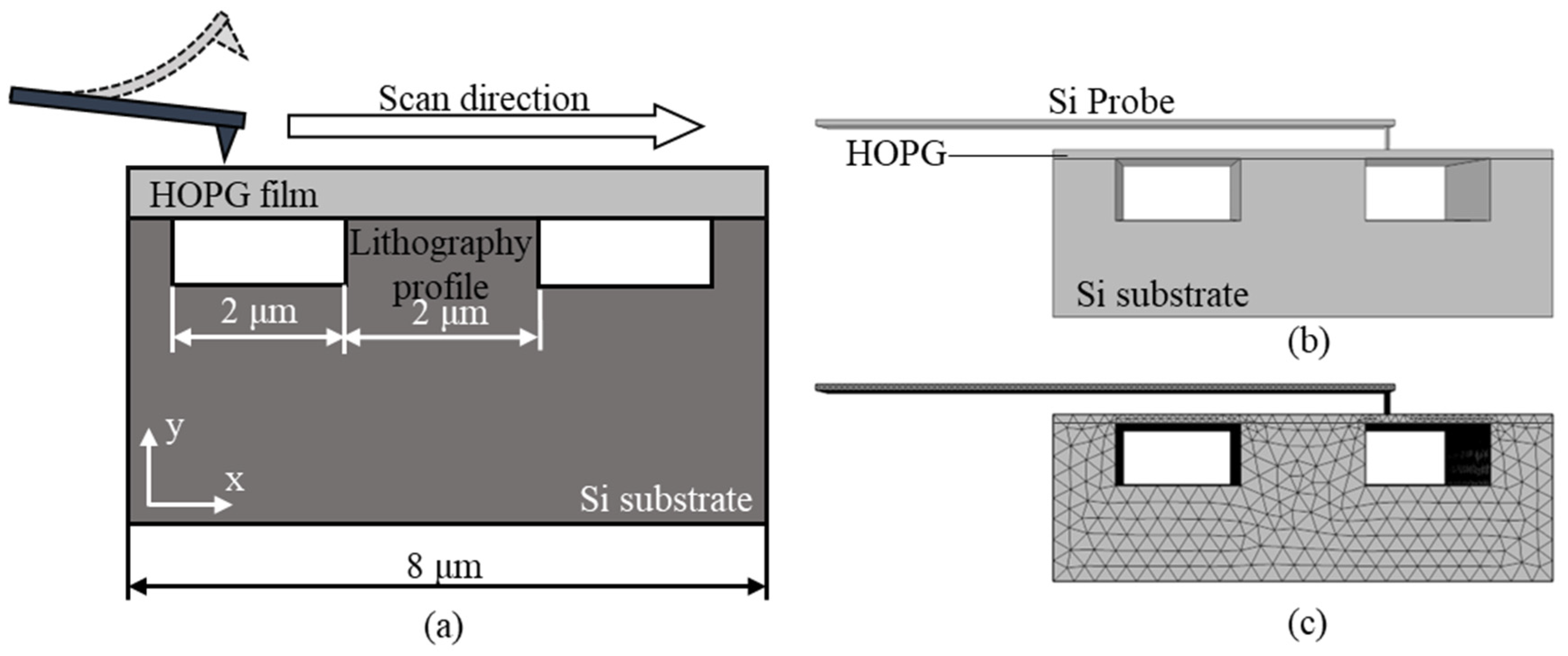
3.1. Finite Element Simulation

Subsurface imaging technology can be realized by detecting various aspects of interaction between the probe tip and the sample, but it is necessary to analyze multi-influence coupling parameters, it will be too complicated to calculate if the modulus is calculated by analytical formula. In this study, the physical model based on the contact between the probe tip and the sample are used to simulate the contact resonance frequency of the vibrating probe scanned over the sample. The physical model and the involved calculation formula have been presented in Section 2.2. In order to compare the simulation results with the specific experimental results, a schematic diagram of the simulation model in Figure 4 is established.
As shown in Figure 4a, the probe is scanned with a distance of 8 μm over the surface of the sample with subsurface microstructures formed by a photolithographic grating with a HOPG film. The width and spacing of the lithographic grooves are 2 μm, and the depth of the grooves is 500 nm. Through the finite element simulation, the contact resonance frequency of the probe can be calculated when the probe scans over each point on the scanning path. The calculated values can then be numerically plotted, which can be used for estimation of the detected sample subsurface topography. The geometric modeling and the meshing of this FEM is shown in Figure 4b. The experimental parameters used in the simulation have also been set as the same as the actual experiment, and shown in Table 2 [17].
The finite element simulation results are revealed in Figure 5. When scanning along the sample surface with different HOPG film thicknesses, the resonance frequencies of the probe-sample contact at each point on the X-axis are shown in Figure 5a. It can be seen clearly that with the increase of the buried depth of the subsurface microstructure, the resonant frequency gradually decreased. The relationship between the buried depth and the maximum frequency difference is shown in Figure 5b. It is easy to find that when the tip is directly above the geometric center of the defect, the resonant frequency of the probe-sample contact is the smallest. Conversely, the probe-sample contact resonance frequency is maximum when the tip is in the absence of defects. The difference between these two frequencies reflects the detection capability of the CR-AFM for defects. When this difference tends to zero, it indicates that the probe is difficult to detect the existence of defects. From Figure 5b, it can be seen that as the buried depth increases, the maximum frequency difference become smaller, showing an exponential downward trend. This phenomenon will be further discussed in conjunction with the experimental results later.

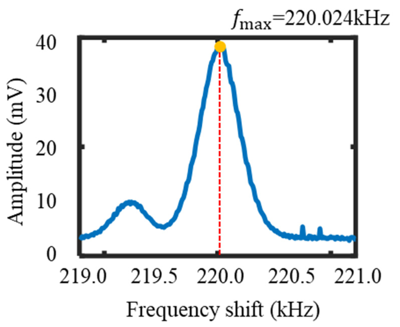
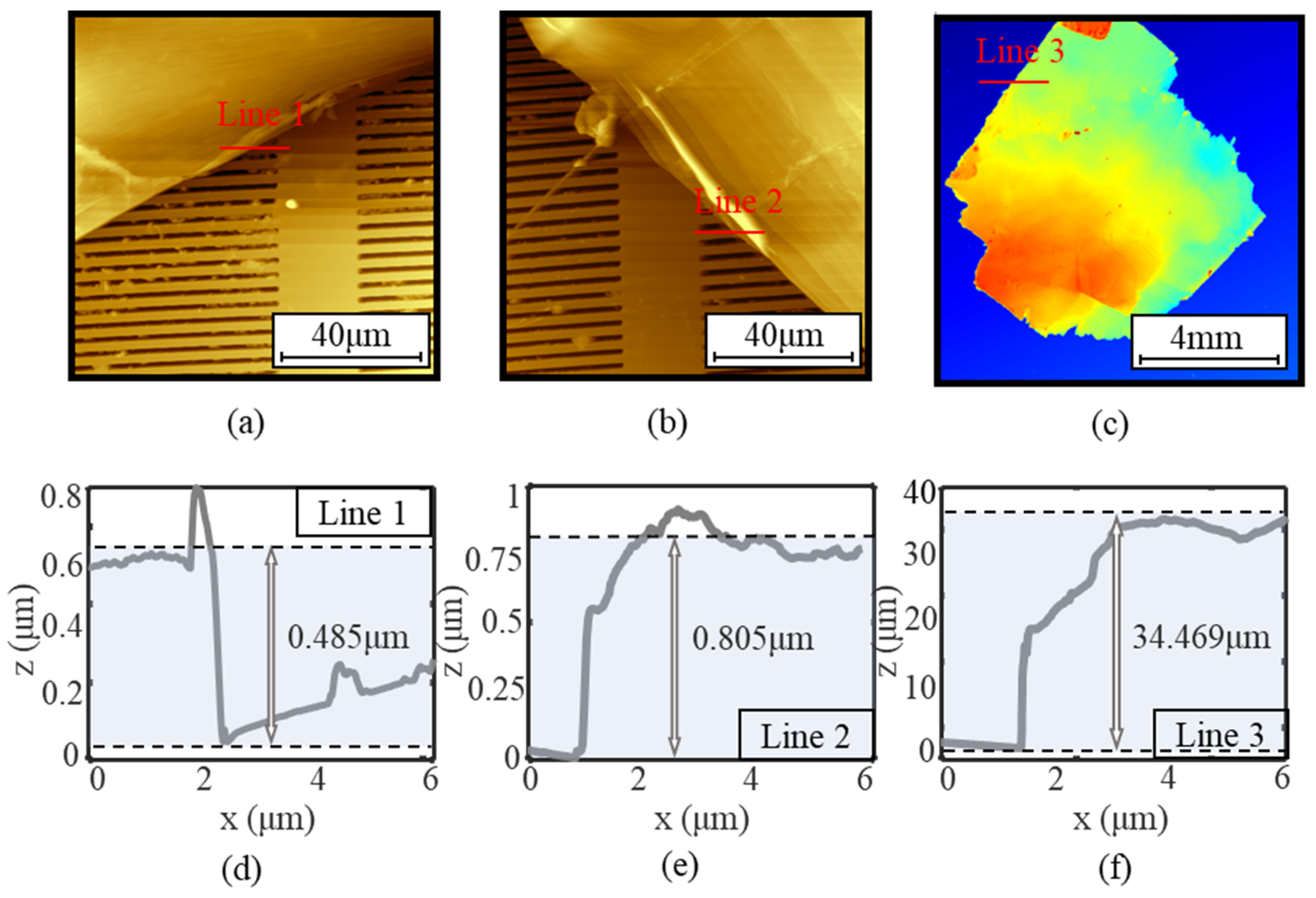
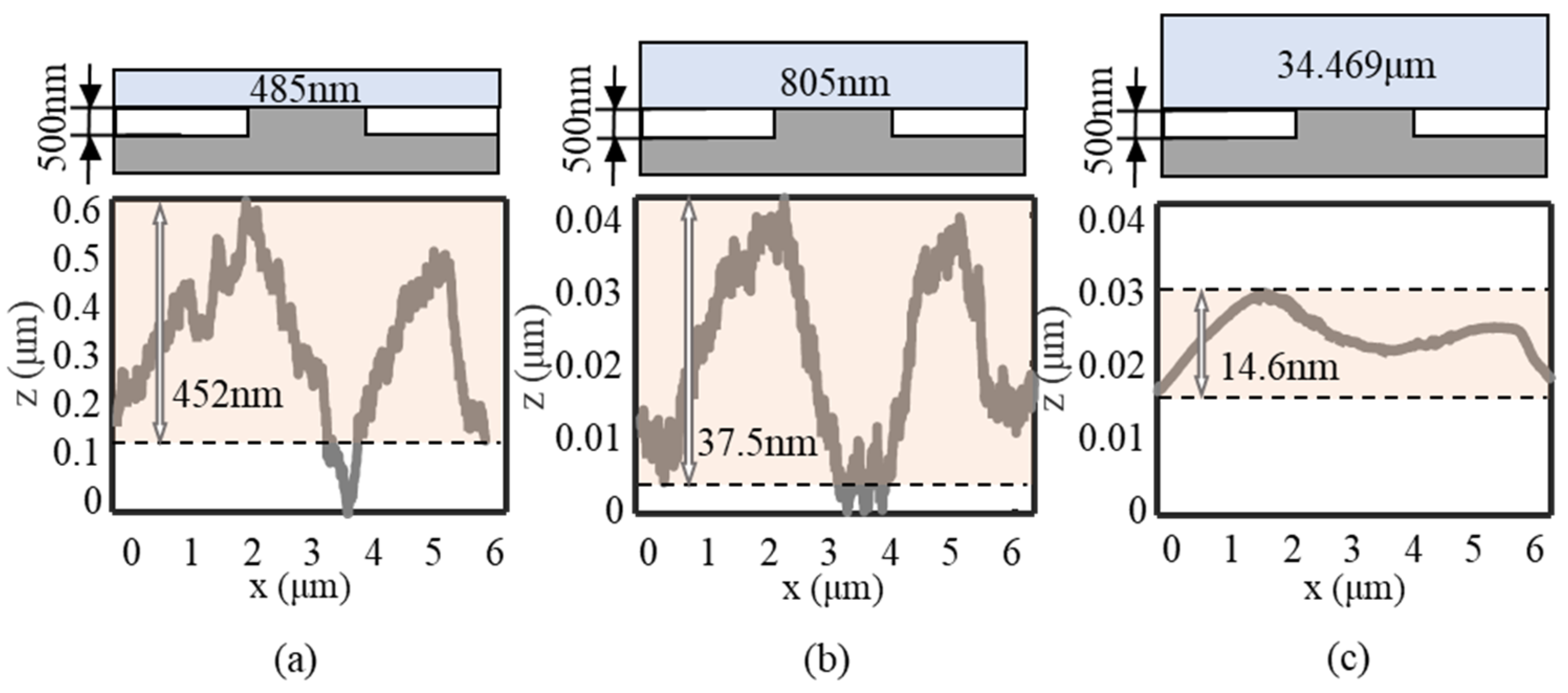
3.2. Experimental Results

Experiments are carried out to demonstrate the capability of the established CR-AFM system. In the experiments, the contact resonance frequency of the probe and the sample is firstly determined by sweeping the excitation signal for driving the probe vibrating. In this experiment, the first-order contact resonance frequency of the probe-sample is determined to be 220 kHz, which is tested by sweeping the frequency of the probe in contact with an unetched silicon wafer covered by a 30 μm HOPG film. The result of the frequency sweep on the single point is shown in Figure 6. Then, an exciting signal with the frequency of 220 kHz and an amplitude of about 500 mV is applied to the thermally driven probe. First, the probe is brought into contact with the sample, and a sweep signal is applied to the probe to determine the contact resonance frequency between the probe and the sample at a single point. Then, use this frequency as the reference oscillation frequency in the probe scanning process. When the topography of the subsurface changes, the contact resonance frequency of the surface changes, and the vibration frequency of the probe also varies. After that, the difference between the collected real-time probe contact resonance frequency and the reference frequency is used as a feedback signal, and the piezoelectric ceramic is controlled to drive the probe to move up and down to complete the scan process and the probe can trace the subsurface profile in this way. To briefly summarize, the deviation of the actual vibration frequency of the probe from the reference frequency at each measurement point is used as the control signal, and the subsurface morphology of the sample is characterized by the motion profile of the Z-axis piezoelectric ceramic.
Figure 7 shows the characterizations of the three samples used in the experiments. As shown in the figure, the upper figures illustrate the surface topography of the sample. The sectional profile that marked in the upper figures are shown in the lower figures. As the thickness of the sample in Figure 7c is beyond the measurement range of AFM, a white light interferometer was used to measure the HOPG film thickness while AFM is used for the first two samples. The HOPG film thicknesses covered on the three samples were evaluated to be 485 nm, 805 nm and 34.469 μm, respectively. It should be noted that the thickness values are obtained by averaging multiple sectional profile to reduce the estimation random error.
The measurement results of the three samples by the built CR-AFM are shown in Figure 8. The piezoresistive cantilever probe used in the experiment has a resonant frequency of 30 kHz and it has a contact resonance frequency of 220 kHz with the sample surface with subsurface microstructures. The scan rate of the probe is 100 nm/s. The sampling frequency of the scanned point data in the experiment is 1000 kHz and every 100 acquired data are averaged. Three different lines show the displacement of the piezo scanner in Z direction required to keep oscillation frequency of cantilever constant and here, use such curves to show the results of subsurface topography. It can be seen from Figure 8 that the raster-like lines are obtained in the surface scanning of the probe.
Figure 8 studies the impact of different buried depths on the measurement results under the same grating height. The measured grating depths in three scans are 452 nm, 37.5 nm and 14.6 nm, respectively. According to the result, The HOPG film thickness difference between the first sample and the second sample is 365 nm, and the measured subsurface grating depth difference between that is 414.5 nm. Meanwhile, the HOPG film thickness difference between the second sample and the third sample is 33.664 μm, but the measured depth difference is only 22.9 nm. It means that the measured grating depth and the buried depth do not show a simple linear relationship. With the increase of the buried depth of the microstructure, the value of the measured subsurface depth gradually decreases, which verify the aforementioned simulation results. Then, we focused on the result of measuring the width of the subsurface microstructure. It is known that the width of the silicon wafer grating is 2 μm, but the measured slot width of the subsurface microstructure is 3.08 μm that is a little bit larger than 2 μm according to both the simulation and the experimental results. This can be interpreted as the relatively small separation distance between the subsurface microstructures, at this time, the stiffness of the surface location without subsurface microstructure between the intervals of the locations with subsurface microstructure will also be affected by the subsurface microstructure. This means that two adjacent defects will be coupled to each other and act on the stiffness of the surface between them, and finally change the contact resonance frequency of the probe on its surface. It is worth noting that although the three samples in Figure 8 have the same microstructures with different buried depths of, the positions of the detected subsurface microstructures are almost the same, demonstrating the capability of the CR-AFM to detect the subsurface microstructures. Even if the thickness of the HOPG film (buried depth of the subsurface microstructure) reaches a large value of 34.469 μm, it is possible to detect the location of the subsurface microstructures by the developed CR-AFM.

4. Summary

In this paper, a CR-AFM based measurement method is developed for detection of subsurface microstructures with micrometric sizes and relatively large buried depths. A simulation model is established by clarifying the relationship between resonance frequency and contact stiffness of the probe-sample system. A new prototype CR-AFM is established for experiments. The experimental results have good agreement with the simulation results. The resonance frequency feedback method used in this study is different from the traditional CR-AFM using contact force as the feedback signal. Owing to the larger buried depth measurement capability proposed in this study, a subsurface grating microstructure with a feature size of 2 μm, a feature depth of 0.5 μm and a buried depth of 34 μm has been successfully measured by the proposed method. The measured buried depth of subsurface microstructure is almost two orders larger than that of the traditional method, demonstrating its potential advantage over the ultrasonic detection technique and the traditional ultrasonic AFM technique.
In addition, it should be noted that since the scanning method is operated based on the resonance frequency instead of the constant force, it may cause damage to the sample surface, thus reduction of surface damage caused by the scanning would be studied as a future work. It should be also noted that the influence of the film thickness variation on the scanning results is ignored in this study because of the short scanning range, and the uniformity of the film thickness in a large range could generate additional influence on the measurement of subsurface topography, thus elimination of the influence of the film thickness uniformity on subsurface topography measurement associated with a large range scanning would be also investigated in the future work.

Author Contributions

Conceptualization, Y.-L.C.; Data curation, C.W., J.T. and M.D.; Formal analysis, J.C.; Funding acquisition, B.-F.J. and Y.-L.C.; Investigation, B.-F.J.; Methodology, Y.-L.C.; Writing—original draft, Y.W.; Writing—review & editing, Y.-L.C. All authors have read and agreed to the published version of the manuscript.

Funding

This work was supported in part by the by the National Natural Science Foundation of China under Grant 51975522, National Key R&D Program of China under Grant 2020YFB2007600, in part by the Ministry of Industry and Information Technology’s Manufacturing High-quality Development Project under Grant TC200H02J. The work of B.F. Ju was supported in part by the National Natural Science Foundation of China under Grant 52035013 and Grant U1709206, in part by the Science Fund for Creative Research Groups of National Natural Science Foundation of China under Grant 51821093, and in part by the Zhejiang Provincial Key R&D Program of China under Grant 2018C01065. (Corresponding author: Yuan-Liu Chen.)

Conflicts of Interest

The authors declare no conflict of interest.

References

  1. Fang, F.Z.; Zhang, X.D.; Gao, W.; Guo, Y.B.; Byrne, G.; Hansen, H.N. Nanomanufacturing—Perspective and applications. CIRP Ann. 2017, 66, 683–705. [Google Scholar] [CrossRef] [Green Version]
  2. Uhlmann, E.; Mullany, B.; Biermann, D.; Rajurkar, K.P.; Hausotte, T.; Brinksmeier, E. Process chains for high-precision components with micro-scale features. CIRP Ann. 2016, 65, 549–572. [Google Scholar] [CrossRef]
  3. Shore, P.; Cunningham, C.; DeBra, D.; Evans, C.; Hough, J.; Gilmozzi, R.; Kunzmann, H.; Morantz, P.; Tonnellier, X. Precision Engineering for Astronomy and Gravity Science. CIRP Ann.-Manuf. Technol. 2010, 59, 694–716. [Google Scholar] [CrossRef]
  4. Jawahir, I.S.; Brinksmeier, E.; M’Saoubi, R.; Aspinwall, D.K.; Outeiro, J.C.; Meyer, D.; Umbrello, D.; Jayal, A.D. Surface Integrity in Material Removal Processes: Recent Advances. CIRP Ann.-Manuf. Technol. 2011, 60, 603–626. [Google Scholar] [CrossRef]
  5. Thakur, A.; Gangopadhyay, S. State-of-the-art in Surface Integrity in Machining of Nickel-based Super Alloys. Int. J. Mach. Tools Manuf. 2016, 100, 25–54. [Google Scholar] [CrossRef]
  6. Chen, Y.-L.; Wang, S.; Shimizu, Y.; Ito, S.; Gao, W.; Ju, B.F. An In-process Measurement Method for Repair of Defective Microstructures By Using a Fast Tool Servo. Precis. Eng. 2015, 39, 134–142. [Google Scholar] [CrossRef] [Green Version]
  7. Yan, J.; Asami, T.; Harada, H.; Kuriyagawa, T. Crystallographic Effect On Subsurface Damage Formation In Silicon Microcutting. CIRP Ann.-Manuf. Technol. 2012, 61, 131–134. [Google Scholar] [CrossRef]
  8. Fang, F.Z. Atomic and Close-to-Atomic Scale Manufacturing—A Trend in Manufacturing Development. Front. Mech. Eng. 2016, 11, 325–327. [Google Scholar] [CrossRef]
  9. Kruth, J.P.; Bartscher, M.; Carmignato, S.; Schmitt, R.; De Chiffre, L.; Weckenmann, A. Computed Tomography for Dimensional Metrology. CIRP Ann.-Manuf. Technol. 2011, 60, 821–842. [Google Scholar] [CrossRef]
  10. Yan, D.; Drinkwater, B.W.; Neild, S.A. Measurement of the Ultrasonic Nonlinearity of Kissing Bonds In Adhesive Joints. NDTE Int. 2009, 42, 459–466. [Google Scholar] [CrossRef]
  11. Yang, X.Y.; Sun, A.; Ju, B.-F.; Xu, S.N. A Rotary Scanning Method To Evaluate Grooves and Porosity for Nerve Guide Conduits Based on Ultrasound Microscopy. Rev. Sci. Instrum. 2018, 89, 073705. [Google Scholar] [CrossRef] [PubMed]
  12. Gao, W.; Aoki, J.; Ju, B.F.; Kiyono, S. Surface profile measurement of a sinusoidal grid using an atomic force microscope on a diamond turning machine. Precis. Eng. 2007, 31, 304–309. [Google Scholar] [CrossRef]
  13. Hurier, M.A.; Wierez-Kien, M.; Mzayek, C.; Donnio, B.; Gallani, J.L.; Rastei, M.V. Nonlinear Phase Imaging of Gold Nanoparticles Embedded in Organic Thin Films. Langmuir 2019, 35, 16970–16977. [Google Scholar] [CrossRef] [PubMed]
  14. Soliman, M.; Ding, Y.; Tetard, L. Nanoscale Subsurface Imaging. J. Phys.-Condens. Matter 2017, 29, 173001. [Google Scholar] [CrossRef] [PubMed]
  15. Perrin, A.P.; Ryu, Y.; Amo, C.; Morales, M.; Garcia, R. Subsurface Imaging of Silicon Nanowire Circuits and Iron Oxide Nanoparticles with Sub-10 nm Spatial Resolution. Nanotechnology 2016, 27, 275703. [Google Scholar] [CrossRef] [Green Version]
  16. Zhang, W.; Chen, Y.; Liu, H.; Zheng, L. Subsurface Imaging of Cavities in Liquid by Higher Harmonic Atomic Force Microscopy. Appl. Phys. Lett. 2018, 113, 193105. [Google Scholar] [CrossRef]
  17. Ma, C.; Chen, Y.; Arnold, W.; Chu, J. Detection of subsurface cavity structures using contact-resonance atomic force microscopy. J. Appl. Phys. 2017, 121, 154301. [Google Scholar] [CrossRef]
  18. Ma, C.; Arnold, W. Nanoscale ultrasonic subsurface imaging with atomic force microscopy. J. Appl. Phys. 2020, 128, 180901. [Google Scholar] [CrossRef]
  19. Wang, T.; Ma, C.F.; Hu, W.; Chen, Y.H.; Chu, J.R. Visualizing Subsurface Defects in Graphite by Acoustic Atomic Force Microscopy. Microsc. Res. Tech. 2017, 80, 66–74. [Google Scholar] [CrossRef]
  20. Wagner, R.; Moon, R.J.; Raman, A. Mechanical properties of cellulose nanomaterials studied by contact resonance atomic force microscopy. Cellulose 2016, 23, 1031–1041. [Google Scholar] [CrossRef]
  21. Cadena, M.J.; Chen, Y.; Reifenberger, R.G.; Raman, A. Sub-surface AFM imaging using tip generated stress and electric fields. Appl. Phys. Lett. 2017, 110, 123108. [Google Scholar] [CrossRef]
  22. Yamanaka, K.; Noguchi, A.; Tsuji, T.; Koike1, T.; Goto, T. Quantitative Material Characterization by Ultrasonic AFM. Surf. Interface Anal. 1999, 27, 600–606. [Google Scholar] [CrossRef]
  23. Yamanaka, K.; Nakano, S. Ultrasonic Atomic Force Microscope with Overtone Excitation of Cantilever. Jpn. J. Appl. Phys. 1996, 35, 3787–3792. [Google Scholar] [CrossRef]
  24. Rabe, U.; Janser, K.; Arnold, W. Vibrations of free and surface-coupled atomic force microscope cantilevers: Theory and experiment. Rev. Sci. Instrum. 1996, 67, 3281–3293. [Google Scholar] [CrossRef]
  25. Parlak, Z. Quantitative Imaging of Subsurface Structures and Mechanical Properties at Nanoscale Using Atomic Force Microscope; Georgia Institute of Technology: Atlanta, GA, USA, 2010. [Google Scholar]
  26. Sharahi, H.J.; Shekhawat, G.; Dravid, V.; Park, S.; Egberts, P.; Kim, S. Contrast mechanisms on nanoscale subsurface imaging in ultrasonic AFM: Scattering of ultrasonic waves and contact stiffness of the tip-sample. Nanoscale 2017, 9, 2330–2339. [Google Scholar] [CrossRef]
  27. Gorantla, S.; Bachmatiuk, A.; Hwang, J.; Alsalman, H.A.; Kwak, J.Y.; Seyller, T.; Eckert, J.; Spencer, M.G.; Rümmeli, M.H. A universal transfer route for graphene. Nanoscale 2014, 6, 889–896. [Google Scholar] [CrossRef] [Green Version]
  28. Kang, J.; Shin, D.; Bae, S.; Hong, B.H. Graphene transfer: Key for applications. Nanoscale 2012, 4, 5527–5537. [Google Scholar] [CrossRef]
Figure 1. Schematic of the CR-AFM for measuring subsurface microstructures.
Applsci 12 05460 g001
Figure 2. (a) The simplified model of contact between the probe tip and the sample. (b) The simplified model for cantilever probe in contact with sample surface.
Applsci 12 05460 g002
Figure 3. The prototype CR-AFM system used in experiments.
Applsci 12 05460 g003
Figure 4. (a) Schematic of the simulation model. (b) shows the geometry model of finite element simulation and (c) shows the meshing for finite element simulation.
Applsci 12 05460 g004
Figure 5. Finite element simulation results. (a) shows the change in the contact resonance frequency of the probe sweeping across the sample surface of 8 μm when the surface HOPG film thickness is different. (b) shows the variation of the maximum contact resonance frequency difference during the scanning process with the increase of the HOPG film thickness.
Applsci 12 05460 g005
Figure 6. The spectrum of the contact resonant frequency around a local maximum at the start point of the experiment.
Applsci 12 05460 g006
Figure 7. Characterization of the three samples prepared in the experiments. (a,b) show the AFM scan images at the edge of the HOPG films with two different film thicknesses covered on the Si substrates. (c) shows the white light interference image of the third sample with a different film thickness from the first two samples. (df) show the height difference of samples (ac) on line 1, line 2, and line 3, respectively.
Applsci 12 05460 g007
Figure 8. The measurement results of subsurface microstructures using the CR-AFM. (ac) show the subsurface line scan results of the samples with 485 nm, 805 nm, and 34.469 μm HOPG film thicknesses, respectively.
Applsci 12 05460 g008
Table 1. Property parameters of the probe.
Tip MaterialTip RadiusTip HeightResonant Frequency
Si<15 nm4.5~4.6 μm30 kHz
Table 2. Experimental parameters used in the simulation.
ParametersValues
Tip Radius10 nm
Tip Height5 μm
Tip Spring Constant300 N/m
Tip Length110 μm
Tip Width50 μm
Contact Force10 nN
Si Density 2330   kg / m 3
HOPG Density 2270   kg / m 3
Elastic Modulus of Si190 Gpa
Elastic Modulus of HOPG18 Gpa
Poisson’s Ratio of Si0.2782
Poisson’s Ratio of HOPG0.25
Publisher’s Note: MDPI stays neutral with regard to jurisdictional claims in published maps and institutional affiliations.

