Abstract
NFinFET transistors with various fin widths (110 nm, 115 nm, and 120 nm) are put into measurements, and the data are collected. By using the modified model, the measure data is fitted. Several parameters in the formula of modified model are determined to make both the measured data and the fitting data almost as close as possible. Those parameters are listed and analyzed, including kN (proportional to channel width and gate oxide capacitor, and inversely proportional to the channel length) λ (the inverse of Early Voltage), and sometimes Vth (Threshold Voltage). By kN, the appropriate process control can be high lighted, the corresponding channel concentration can be calculated and thus many implicit physical quantities may be exploited.
1. Introduction
Source-Drain leakage current, known as one of the short channel effects, is successfully suppressed on FinFET transistors. The structure of FinFET looks like an emerging 3-dimensional “I” character with Source and Drain as the two ends and the channel in between. The applied bias on Gate poly-silicon crossing over the channel depletes the whole slim channel and builds up a barrier in between Source and Drain, which thus blocks or prevents the possibility of leakage current. The process is achieved because of the good conformality (step coverage) of chemical vapor deposition by flowing SiH4 (silane) at chosen flow rate under certain pressure at an appropriate temperature in kinetic regime for a good deposition rate [1,2,3,4,5].
Furthermore, the electrical performance of FinFET transistors may be also enhanced either by high dielectric constant gate oxide or by high mobility channel. On one hand, the capacitance of the gate capacitor is to be raised if the dielectric of the gate oxide, mainly silicon dioxide, can be replaced with Hf-mixed tantalum oxide whose dielectric constant is about 5 times of that of N-mixed silicon dioxide. For instance, 90 nm-process devices can be equivalently reduced to 14 nm-process devices, which is quite encouraging once the process is production-worthy. On the other hand, the mobility of silicon channel may be promoted by even 2.5 to 4 times as SiGe is technically and sophisticatedly introduced stack by stack. The above advanced techniques and other options are definitely promising and achievable, making FinFET continuously popular as currently [6,7,8,9,10,11,12].
However, the electrical performances, mainly manifested in current-versus-voltage characteristic curves (I–V curves), are thus put to be parameter-extracted in the model, which takes advantage of sophisticated equivalent circuits for academic and industrial uses. Nevertheless, the measured I–V curves are speculated to be also fitted by the “modified” conventional formula [13,14,15,16,17,18].
In this study, the “modified” conventional I–V characteristic curve formula naively generates fitting data to fit as measured (IDS, VDS) and (IDS, VGS) data by choosing appropriate parameter values, such as the threshold voltage (Vth), lambda (λ) which is inversely proportional to the absolute value of Early Voltage (VA), and kN which is proportional to the total width of the channel and inversely proportional to the channel length.
2. Preparation and Measurements
2.1. Preparation
The epi-silicon layer is deliberately ionic dry etched with various 3-dimensional sizes, such as 110 nm, 115 nm, and 120 nm wide and corresponding 9 times high fin channel. On both ends of the channel are Source and Drain, looking like a letter “I”. The epi-silicon fin channel is grown with ultra thin gate oxide and covered with arsenic heavily doped poly-silicon.
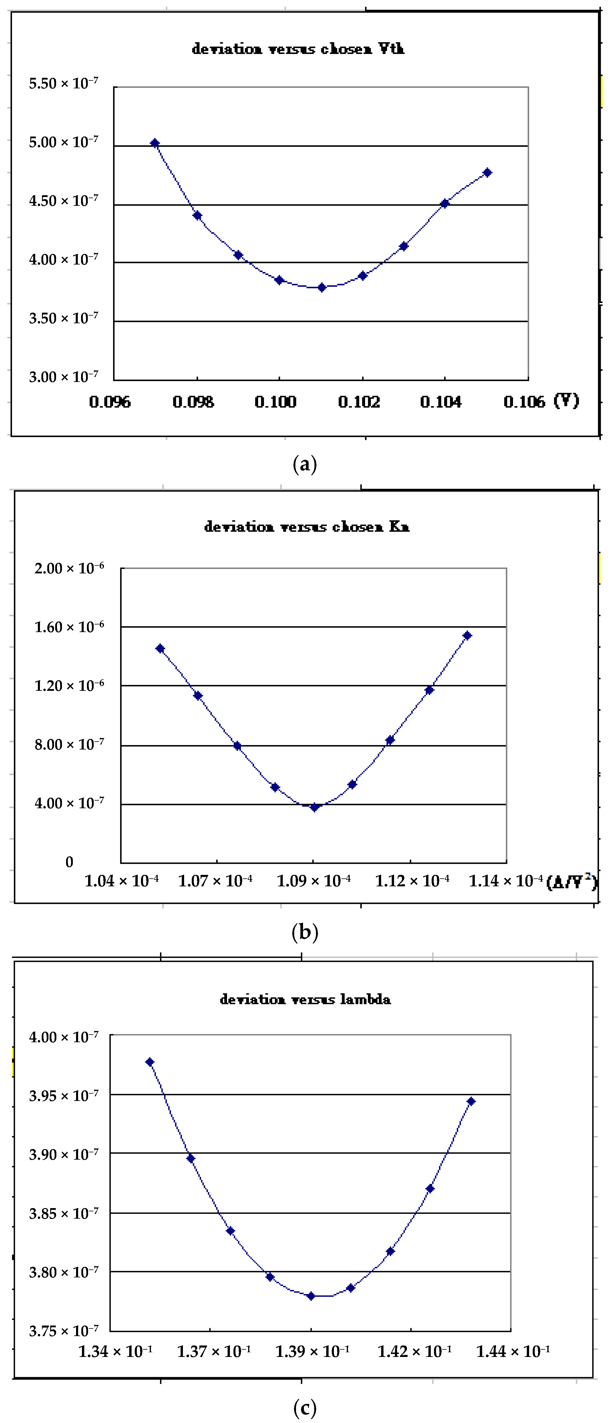
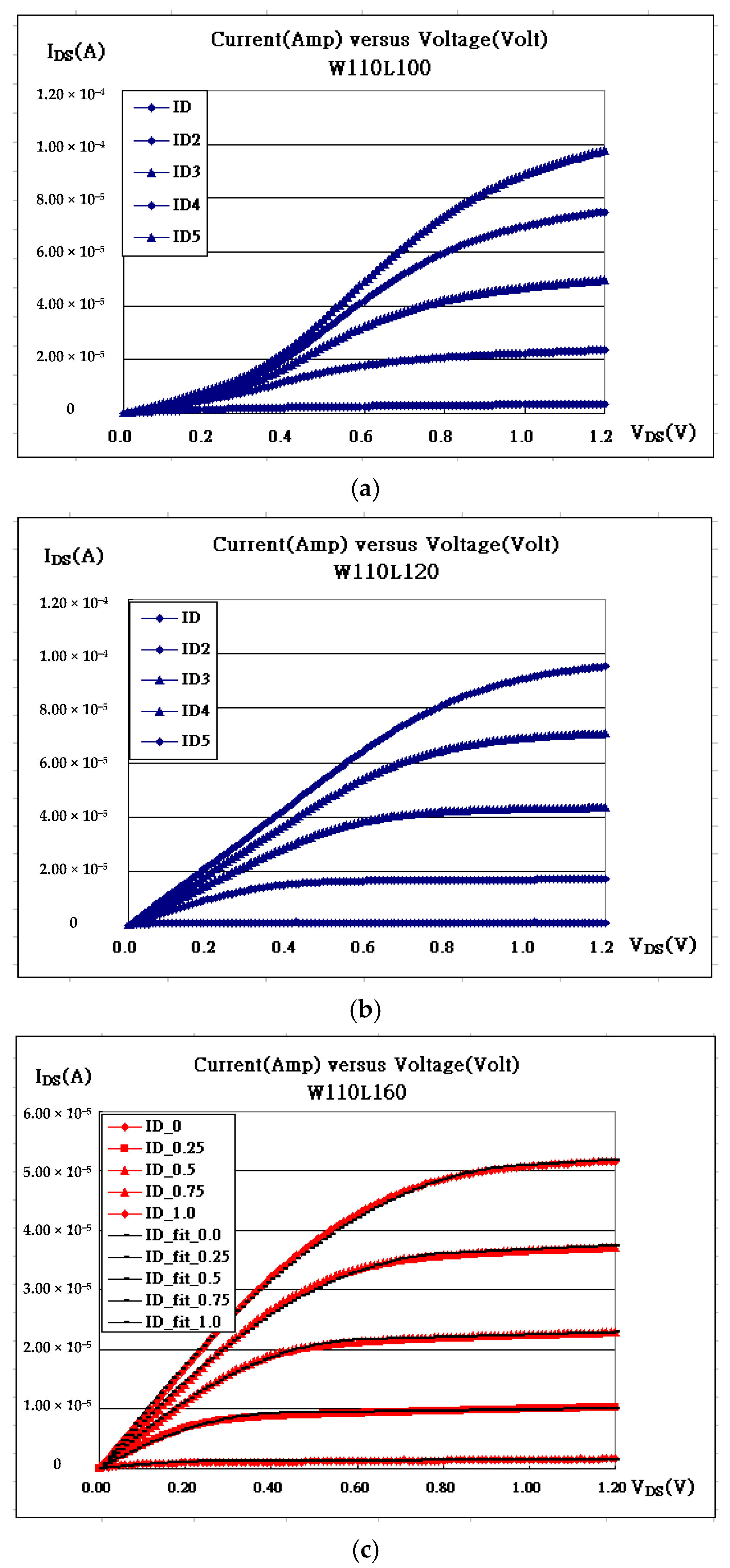
2.2. Fitting IDS-VDS and IDS-VGS
The two-regime modified conventional formulas for FinFET transistors are expressed in the following:
where
where VA is Early Voltage, Cox is gate oxide capacitance, and Weff = 19Wo.
Equation (1) works as VDS is less than (VGS − Vth) while Equation (2) works as VDS is larger than (VGS − Vth). And those parameters are predominantly determined to minimize the deviation (delta, δ) as follows in Equation (3):
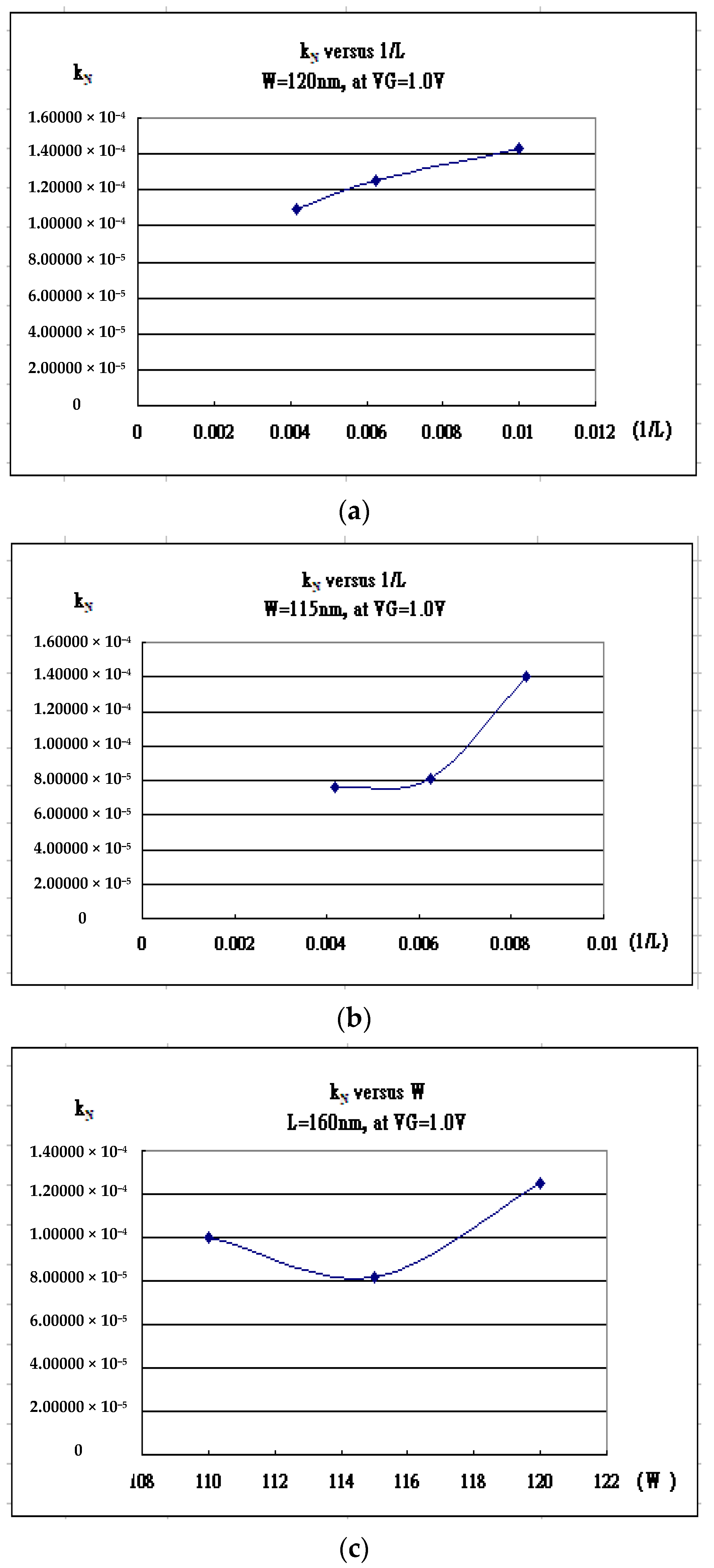
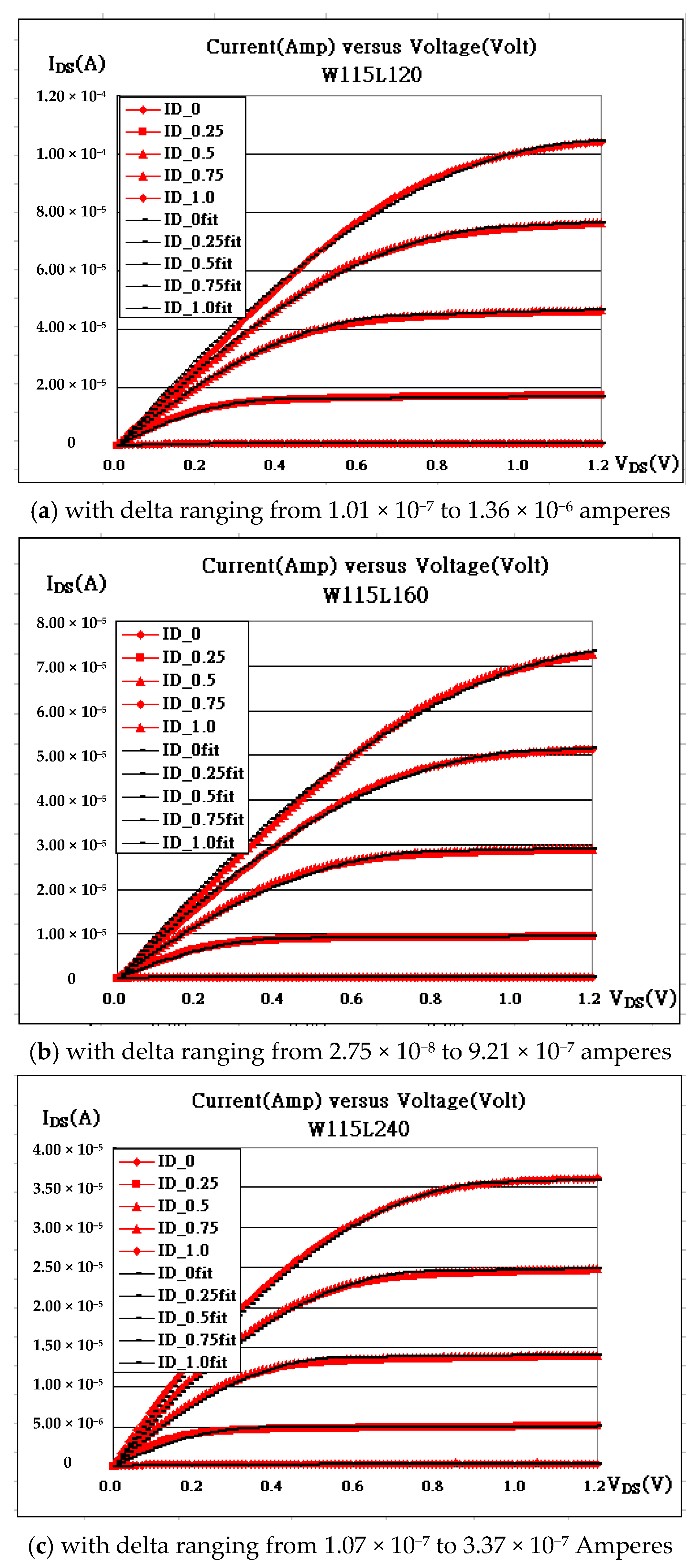
3. Results and Discussion
The minimum deviation (delta, δ in Equation (3) is used to determine the chosen parameters. For example, the measured characteristic curve on the device denoted by W120L240 (fin width = 120 nm, channel length = 240 nm) at VG = 1.0 V may be well fitted by choosing the three parameters Vth = 0.101 V, kN = 1.09 × 10⁻⁴ A/V2, and lambda = 0.139 in Equations (1) and (2) as shown in Figure 1a–c, where the minimum deviation value is found to be 3.79569 × 10⁻⁷ A.
Figure 1.
Three parameters (Vth, Kn, lambda) at VG = 1.0 V on W120L240 (fin width = 120 nm, and channel length = 240 nm) are determined through minimum deviation technique with the minimum deviation = 3.79569 × 10⁻⁷ A at (a) Vth = 0.101 V as in deviation versus Vth, (b) kN = 1.09 × 10⁻⁴ A/V2 as in deviation verses kN, and (c) lambda = 0.139 as in deviation versus lambda.
Therefore by using the same skill, all the parameters in Equations (1) and (2) are determined to fit the measured characteristic curves except the ones in Figure 2a,b. where the two transistors, denoted by W110L100 (Fin width = 110 nm, Channel length = 100 nm) and W110L120 (Fin width = 110 nm, Channel length = 120 nm), do not look like FET and are not worth fitting. All the other fitting results are shown in Figure 2c, Figure 3a–c and Figure 4a–c. The final minimum delta’s at various VG’s. range from 3.25 × 10⁻⁸ Ampere to 1.36 × 10⁻⁶ Ampere, which are engineering acceptable.
Figure 2.
IDS-VDS characteristic curves and the corresponding fitting, including (a) W110L100, (b) W110L120, (c) W110L160.
Figure 3.
IDS-VDS characteristic curves and the corresponding fitting, including (a) W115L120, (b) W115L160, (c) W115L240.
Figure 4.
IDS-VDS characteristic curves and the corresponding fitting, including (a) W120L110, (b) W120L160, and (c) W120L240.
In addition, all determined kN’s may be specifically listed as in Table 1, Table 2 and Table 3 at different sizes and at different VG’s [12]. In the modified conventional formula in Equations (1) and (2), kN is supposed to be inversely proportional to the channel length. And kN is also proportional to the channel width (Wchannel) and, thus the width of the fin (Wfin), because Wchannel = (9 + 9 + 1) Wfin = 19Wfin. If kN is plotted against Wfin or 1/Lchannel, straight lines are then expected. Unfortunately, most of them fail the testing except on the devices with fin width = 120 nm at VG = 1.0 V partly as found in Figure 5. Of course, at VG = 0.0 V, the transistors, which are still on and may have pretty low threshold voltage or even negative one, are not discussed in this paper. So the applied voltages to Gates depleting the fin channels and making the devices less leaky draw much attention. In Figure 4a, the straight line proves the feasibility at VG = 1.0 V with fin width = 120 nm, while the other two graphs, Figure 4b,c do not. The non-straight lines might be due to either over-depletion or under-depletion. Over-depletion means that the depletion regions from both sides of the fin overlap resulting to disturbing the blocking function. On the other hand, the depletion regions do not completely cover all the fin for under-depletion and the leakage current gets apparent.
Table 1.
kN values with Fin Width = 120 nm.
Table 2.
kN values with Fin Width = 115 nm.
Table 3.
kN values with Fin Length = 160 nm.
Figure 5.
kN is supposed to be proportional to the channel width or the inverse of channel length. (a) kN versus 1/L with fin width = 120 nm, (b) kN versus 1/L with fin width = 115 nm, and (c) kN versus W with channel length = 160 nm.
The three transistors with 120 nm fin width at VG = 1.0 V provide valuable information, i.e., the whole fin may be totally depleted without interference from the other side of the applied bias. One or the other side of the applied Gate bias depleted 60 nm, which is a half of the fin width, as shown in Figure 6, where the energy band appears with 1.12 eV energy gap. The so-called p-type channel or substrate is interpreted as boron dopants-in the silicon lowering the Fermi energy. Once the applied Gate bias bents the intrinsic Fermi energy down below the Fermi energy, the region becomes strongly inversed to n-type semi-conductor making the channel conductive. The thickness of the conductive layer may as well be calculated by solving Maxwell’s Equations as stated in Equations (4) and (5) with W set to 60 nm. The channel concentration is then estimated to be p = 3.66 × 10²³ (m−3), which is substituted into (KBT) ln(p/ni) to obtain 0.438 eV (energy difference between EF(i) and EF). Therefore, the strong inversion layer is determined to be 203 angstroms, which was one half of the parabolic curve (in Equation (4)) in Figure 6, and is surprisingly about one third of the whole fin width.
where
Figure 6.
Silicon energy gap addressing bent intrinsic Fermi Energy, p-type Fermi Energy, and the strong-inversed layer from p-type to n-type.
4. Conclusions
The modified conventional current-voltage formula has demonstrated the fitting capability of the electrical characteristic curves. Once the parameters are determined through engineering fitting, those parameters are advisable to understand the implicit physics underlying the FET transistor. The current-voltage characteristic fitting simply obeys the modified formula in Equations (1) and (2) and bases on the minimum deviation without first considering the underlying physics. After all crucial parameters, e.g., kN, Vth, and lambda, are determined, the analyses were available. In this paper, kN in Equations (1) and (2) was deliberately examined first, and the thickness of the layer associated with strong inversion is then successfully solved. At the same time, Vth and lambda offering some more information about depletion region and leakage current may be actually expected.
Nevertheless, the model, conventionally established much earlier many decades ago, has been using equivalent circuits to approach to the measured data, and enjoy many fruitful achievements [17]. But tedious work and convergence still have to be taken into account.
In a word, fitting skill proposes another possibility to analyze the transistor. Many approaches, such as lambda corresponding to leakage current, the common threshold voltage requirement, and the common kN requirement, are to be associated with one another. Those analyses are quite intriguing and will be discussed in the near future.
Author Contributions
Conceptualization, H.-C.Y. and S.-C.C.; methodology, H.-C.Y. and S.-C.C.; software, H.-C.Y. and S.-C.C.; validation, H.-C.Y. and S.-C.C.; formal analysis, H.-C.Y. and S.-C.C.; investigation, H.-C.Y. and S.-C.C.; resources, H.-C.Y. and S.-C.C.; data curation, H.-C.Y. and S.-C.C. All authors have read and agreed to the published version of the manuscript.
Funding
This research received no external funding.
Institutional Review Board Statement
Not available.
Informed Consent Statement
Not available.
Data Availability Statement
Not available.
Conflicts of Interest
The authors declare no conflict of interest.
References
- Huang, X.; Lee, W.-C.; Kuo, C.; Hisamoto, D.; Chang, L.; Kedzierski, J.; Anderson, E.; Takeuchi, H.; Choi, Y.-K.; Asano, K.; et al. Sub-50 nm P-channel FinFET. IEEE Trans. Electron. Devices 2001, 48, 880. [Google Scholar] [CrossRef] [Green Version]
- Wang, F.; Xie, Y.; Bernstein, K.; Luo, Y. Dependability analysis of nano-scale FinFET circuits. In Proceedings of the IEEE Computer Society Annual Symposium on Emerging VLSI Technologies and Architectures (ISVLSI’06), Karlsruhe, Germany, 2–3 March 2006; pp. 6, 399. [Google Scholar]
- Takahashi, T.; Beppu, N.; Chen, K.; Oda, S.; Uchida, K. Self-heating effects and analog performance optimization of Fin-type field-effect transistors. Jpn. J. Appl. Phys. 2013, 52, 04CC03. [Google Scholar] [CrossRef]
- Diab, A.; Torres Sevilla, G.-A.; Christoloveanu, S.; Hussain, M.-M. Room to high temperature measurements of flexible SOI FinFETs with sub-20-nm fins. IEEE Trans. Electron. Devices 2014, 61, 3978. [Google Scholar] [CrossRef]
- Chen, C.W.; Wang, S.J.; Hsieh, W.C.; Chen, J.M.; Jong, T.; Lan, W.H.; Wang, M.C. Q-factor Performance of 28 nm-node High-k Gate Dielectric under DPN Treatment at Different Annealing Temperatures. Electronics 2020, 9, 2086. [Google Scholar] [CrossRef]
- Lu, P.; Yang, C.; Li, Y.; Li, B.; Han, Z. Three-Dimensional TID Hardening Design for 14 nm Node SOI FinFETs. Eng 2021, 2, 620–631. [Google Scholar] [CrossRef]
- Wang, S.J.; Sung, S.P.; Wang, M.C.; Huang, H.S.; Chen, S.Y.; Fan, S.K. Electrical stress probing recovery efficiency of 28 nm HK/MG nMOSFETs using decoupled plasma nitridation treatment. Vacuum 2018, 153, 117–121. [Google Scholar] [CrossRef]
- Huang, P.; Ma, C.; Wu, Z. Fast Dynamic IR-Drop Prediction Using Machine Learning in Bulk FinFET Technologies. Symmetry 2021, 13, 1807. [Google Scholar] [CrossRef]
- Crupi, G.; Schreurs, D.M.M.-P.; Caddemi, A.; Angelov, I.; Homayouni, M.; Raffo, A.; Vannini, G.; Parvais, B. Purely analytical extraction of an improved nonlinear FinFET model including non-quasi-static effects. Microelectron. Eng. 2009, 86, 2283–2289. [Google Scholar] [CrossRef]
- Li, Y.; Zhao, F.; Cheng, X.; Liu, H.; Zan, Y.; Li, J.; Zhang, Q.; Wu, Z.; Luo, J.; Wang, W. Four-Period Vertically Stacked SiGe/Si Channel FinFET Fabrication and Its Electrical Characteristics. Nanomaterials 2021, 11, 1689. [Google Scholar] [CrossRef] [PubMed]
- Zhao, E.; Zhang, J.; Salman, A.; Subba, N.; Chan, J.; Marathe, A.; Beebe, S.; Taylor, K. Reliability challenges of high performance PD SOI CMOS with ultra-thin gate dielectrics. Solid State Electron. 2004, 48, 1703–1708. [Google Scholar] [CrossRef]
- Zhao, Z.Q.; Li, Y.; Zan, Y.; Li, Y.L.; Li, J.J.; Cheng, X.H.; Wang, G.L.; Liu, H.Y.; Wang, H.X.; Zhang, Q.Z.; et al. Fabrication technique of the Si0.5Ge0.5 Fin for the high mobility channel FinFET device. Semicond. Sci. Technol. 2020, 35, 045015. [Google Scholar] [CrossRef]
- Yang, H.C.; Liao, K.F.; Tsai, C.Y.; Liao, W.S.; Hsu, F.; Chi, S.C. An Alternative Algorithm to Demonstrate Electrical Characteristics of N/P-Channel Fin-FET Devices. In Proceedings of the 2014 International Conference on Information Science, Electronics and Electrical Engineering, Sapporo, Japan, 26–28 April 2014; pp. 2088–2091. [Google Scholar]
- Wang, M.-C.; Hsieh, W.-C.; Lin, C.-R.; Chu, W.-L.; Liao, W.-S.; Lan, W.-H. High-Drain Field Impacting Channel-Length Modulation Effect for Nano-Node N-Channel FinFETs. Crystals 2021, 11, 262. [Google Scholar] [CrossRef]
- Yang, H.C.; Lu, T.W.; Chang, T.Y.; Chi, S.C. The variation of threshold voltages associated with various applied gate voltages at different temperatures on FinFET devices. In Proceedings of the 2017 International Conference on Applied System Innovation (ICASI), Sapporo, Japan, 13–17 May 2017; pp. 799–801. [Google Scholar]
- Yang, H.C.; Chen, R.S.; Yang, Y.Y.; Tseng, C.K.; Tsai, C.J.; Tseng, J.J.; Chi, S.C.; Liao, Y.J. Electrical Performances of NFinFET and PFinFET Transistors Correlating Processing Conditions and Scales of the Fin Structure. In Proceedings of the 2019 8th International Conference on Innovation, Communication and Engineering (ICICE), Zhengzhou, China, 25–30 October 2019; pp. 55–58. [Google Scholar]
- Lee, J.; Park, T.; Ahn, H.; Kwak, J.; Moon, T.; Shin, C. Prediction Model for Random Variation in FinFET Induced by Line-Edge-Roughness (LER). Electronics 2021, 10, 455. [Google Scholar] [CrossRef]
- Yang, H.C.; Yang, P.J.; Lin, C.C.; Chen, K.H.; Lin, Y.S.; Chi, S.C. Current Voltage Characteristic Curves Addressing Non-Linear Kink-like Effects. In Proceedings of the 2021 7th International Conference on Applied System Innovation (ICASI), Chiayi, Taiwan, 24–25 September 2021; pp. 112–114. [Google Scholar]
Publisher’s Note: MDPI stays neutral with regard to jurisdictional claims in published maps and institutional affiliations. |
© 2022 by the authors. Licensee MDPI, Basel, Switzerland. This article is an open access article distributed under the terms and conditions of the Creative Commons Attribution (CC BY) license (https://creativecommons.org/licenses/by/4.0/).