Review

A Review of the Synthesis, Properties, and Applications of Bulk and Two-Dimensional Tin (II) Sulfide (SnS)

1
Department of Materials, The University of Manchester, Oxford Road, Manchester M13 9PL, UK
2
Department of Chemistry, The University of Manchester, Oxford Road, Manchester M13 9PL, UK
*
Author to whom correspondence should be addressed.
Appl. Sci. 2021, 11(5), 2062; https://doi.org/10.3390/app11052062
Submission received: 22 January 2021 / Revised: 12 February 2021 / Accepted: 14 February 2021 / Published: 26 February 2021
(This article belongs to the Special Issue Applications of 2D Semiconductors)

Abstract

:
Tin(II) sulfide (SnS) is an attractive semiconductor for solar energy conversion in thin film devices due to its bandgap of around 1.3 eV in its orthorhombic polymorph, and a band gap energy of 1.5–1.7 eV for the cubic polymorph—both of which are commensurate with efficient light harvesting, combined with a high absorption coefficient (10−4 cm−1) across the NIR–visible region of the electromagnetic spectrum, leading to theoretical power conversion efficiencies >30%. The high natural abundance and a relative lack of toxicity of its constituent elements means that such devices could potentially be inexpensive, sustainable, and accessible to most nations. SnS exists in its orthorhombic form as a layer structure similar to black phosphorus; therefore, the bandgap energy can be tuned by thinning the material to nanoscale dimensions. These and other properties enable SnS applications in optoelectronic devices (photovoltaics, photodetectors), lithium- and sodium-ion batteries, and sensors among others with a significant potential for a variety of future applications. The synthetic routes, structural, optical and electronic properties as well as their applications (in particular photonic applications and energy storage) of bulk and 2D tin(II) sulfide are reviewed herein.

1. Introduction

Tin(II) sulfide (SnS) is a binary main group metal chalcogenide semiconductor which favours a layered orthorhombic crystal structure [1], occurring naturally as the mineral Herzenbergite (vide infra), which is structurally analogous to germanium sulfide (GeS) at room temperature [1,2]. An orthorhombic, distorted NaCl-type (D2h16: Pnma) polymorph with lattice parameters of a = 4.32, b = 11.20 and c = 3.98 Å is also known [3]. SnS layers are bound by weak van der Waals forces, which provide a chemically inert surface devoid of dangling bonds and surface density of states with no Fermi level pinning at the semiconductor surface. This provides SnS with a high level of environmental and chemical stability, even in acidic solutions [4].
Tin(II) sulfide has emerged as an alternative solar absorber material to conventional thin film absorbers such as cadmium telluride (CdTe) and copper indium gallium selenide (CIGS), due to several properties including biological non-toxicity. Tin and sulfur are also both environmentally benign elements which are cheap and abundant in nature. SnS has an ideal bandgap for solar absorption (1.3 eV for bulk), a high absorbance coefficient >10−4 cm−1, Hall mobility up to 100 cm2 Vs−1 or higher, and tuneable carrier densities in the range of 1015 to 1018 cm−3 [5,6,7]. Due to these exciting properties, it has been incorporated into thin film solar cell architecture alongside a range of electron and hole transporting materials. Theoretically, it has been predicted that the maximum power conversion efficiency (PCE) for SnS-based single junction thin film solar cells could reach a value of 32%; however, in practice, only 4.4% has been achieved so far [8]. Additionally, SnS has also been used as a substitute for platinum as a counter electrode (CE) in dye-sensitised solar cells (DSSCs) [9,10]. Platinum (Pt) has been extensively used as a benchmark CE material due to its excellent catalytic activity, high electrical conductivity, and chemical stability [11]. However, due to the high cost, low natural abundance and the possibility of corrosion by iodide/triiodide (I/I3) redox electrolytes, large scale use of Pt is limited in this application. Several inorganic materials have been explored as replacements for Pt as CEs in dye sentised solar cells (DSSCs). Significant work has been focused on materials such as CoS [12], MoS2 [13], WS2 [14], NiS [15], and NiSe2 [16]. Chalcogenides such as these have unique properties, such as material diversity, abundance, low cost, high catalytic activity and excellent electrical conductivity. However, the use of SnS is becoming more widespread and includes applications in photodetectors [17,18], Li-ion and Na-ion batteries [19,20,21,22], and sensors [23,24], amongst others.

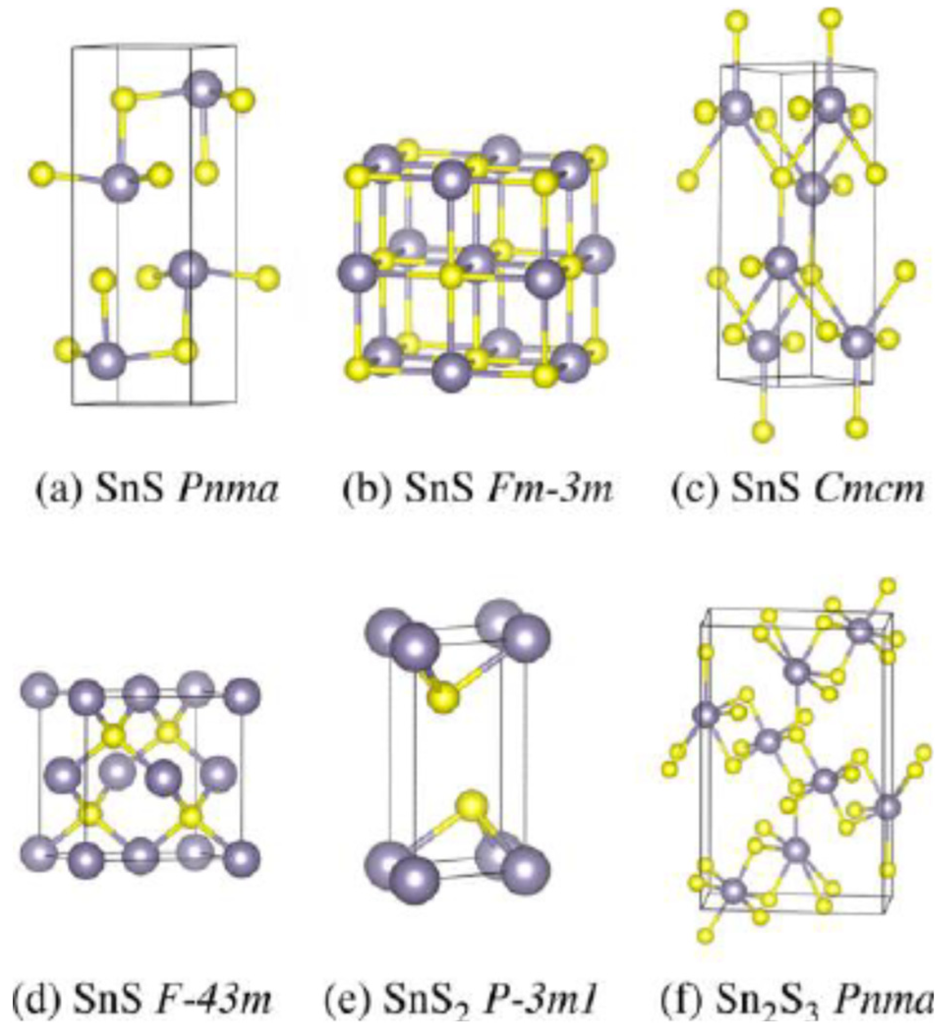
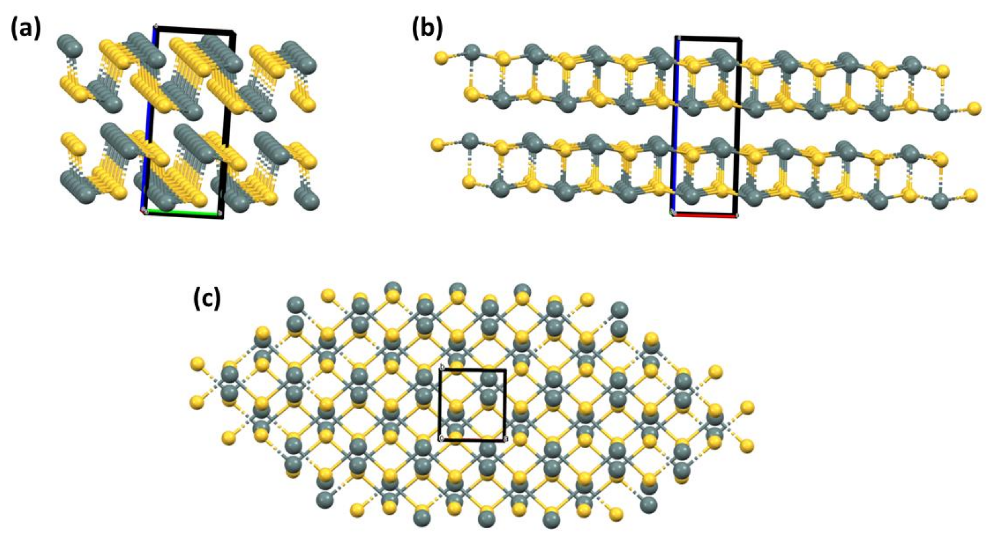
2. Structures and Physical Properties of Tin(II) Sulfide

The most commonly utilised and studied crystalline phase of SnS is the orthorhombic Herzenbergite phase, with the space group Pnma (also reported as Pmcn, see Figure 1). In this structure, the Sn2+ ion coordinates to three S2− ions, with the remaining Sn electrons occupying the vacant position of the tetrahedral geometry as a lone pair of electrons. Bulk orthorhombic SnS has a density of 5.22 g cm−3 and a melting point of 882 °C [25]. Single crystals of SnS typically exhibit p-type conductivity in the range 10−1–10−4 Ω cm−1 [26], although depending on the Sn content, SnS may change its charge-carrying characteristics from p-type to n-type. Bulk band gap energies ranging from 1.20 to 1.37 eV [27] have been reported, with some outlying values as low as 1.07 eV [28]. SnS possesses a thermal conductivity around 1 W m−1 K−1 and a Seebeck coefficient in the range 300–500 µV K−1 [29,30].
Other SnS phases of interest and their respective space groups are Fm3m (rock salt phase), Cmcm (orthorhombic high temperature phase) and F43m (zinc blende phase). The structural and thermodynamic properties of orthorhombic SnS and other polymorphs have been assessed from first-principles calculations. These calculations show good agreement with experimental data, with the exception of zinc blende SnS. This polymorph is predicted to be thermodynamically and kinetically unstable, with a significant discrepancy observed between the calculated and measured lattice parameters for the F43m structure [31]. The Cmcm phase could not be stabilised, because it underwent a second-order phase transition to the thermodynamically stable orthorhombic Pnma structure, which is observed experimentally at 878 K [32]. At normal temperature and pressure, SnS also exhibits a low symmetric stable α-SnS phase. Upon increasing the temperature, α-SnS undergoes a phase transition to a high symmetry β-SnS phase. In simpler terms, orthorhombic SnS undergoes a phase change to a tetragonal structure, with a = 4.23 and c = 11.51 Å [33]. It is reported that the low temperature phase crystallises in a germanium sulfide (GeS)-type structure with the space group Pbnm (D2h16), whereas the higher temperature phase crystallises in the thallium iodide (TlI) type structure with space group Cmcm (D2h17), with the movement of Sn and S along the reference No. 100 direction caused by thermal expansion [34,35]. At a temperature of 878 K (phase transition temperature) the axial ratio of lattice-parameter decreases continuously from a/c >1 to a/c <1. SnS also exists in a cubic π-SnS form, which has been reported by Rabkin et al. The structure was initially determined via electron diffraction methods due to the size and small quantities produced. The cubic lattice parameter was determined to be 11.7 Å [36]. Subsequently, larger scale quantities of π-SnS were prepared by Abutbul et al. Further analysis of this phase via powder XRD showed a cubic lattice parameter a = 11.595 Å. Optical absorption spectroscopy determined an indirect band gap energy of 1.53 eV, in good agreement with density functional theory (DFT) calculations. The DFT calculations also showed that π-SnS is energetically similar to α-SnS, but with a higher stability than the ideal rock salt structure. Raman data showed a shift towards higher energies along with a splitting of the 96 cm−1 peak [37]. π-SnS has been utilised in the production of thin film solar cells by Garcia-Angelmo et al., with a band gap of 1.74 eV and a conductivity of 10−6−1 cm−1 [38]. Table 1 shows compiled crystallographic and calculated data for the structural and thermodynamic parameters for phases of tin sulfide.

3. Synthetic Routes to SnS

To understand the fundamental properties of any material, undoped single crystalline bulk material with negligible defects must first be produced and thoroughly characterised. Chemical vapour transport and the Bridgman–Stockbarger technique are the most commonly used methods for the synthesis of tin(II) sulfide single crystals. To grow high quality single crystals of SnS, one must consider the thermodynamic equilibrium and growth rate (slow growth means high purity, with fast growth rates corresponding to high defect levels). Single crystal growth processes occur at equilibrium; however, it may take several days to allow crystals to reach the equilibrium condition. Once single crystals are grown, these can be used to prepare mono- or few-layer SnS compounds via mechanical or liquid-phase exfoliation. Burton et al. have synthesised single crystals of SnS using chemical vapor transport (CVT). In Table 2, experimental data and density functional theory (DFT) have been used to model the electronic structure and defect chemistry of three different tin chalcogenides (SnS, SnS2 and Sn2S3) [41]. Stoichiometric amounts of tin and sulfur were crushed manually using a pestle and mortar and then placed in a silica ampoule. Iodine was also placed in the same ampule, as recommended by Nitsche et al. [42], and the following chemical process occurs:
S n + S + I 2 S n I 2 + S S n S + I 2
Sorgenfrei et al. have used the Bridgman–Stockbarger technique to produce single SnS crystals [43]. Two approaches were tested: (i) stoichiometric amounts of high purity Sn and S were sealed in a quartz ampoule. The ampoule was placed in a furnace and heated up in steps to 600 °C and left at this temperature until the S had fully reacted. Later, the temperature was increased to 900 °C and maintained for several hours and then switched off, allowing the furnace to cool rapidly. This method gives the pure stoichiometric SnS phases only; and (ii) the two-temperature method, where both Sn and S were kept at two different places within the ampule at two different temperature. The Sn was kept at 600 °C and S was at 200 °C. The reaction took place by evaporating the S; this method reduces the chances of an explosion of the ampoule, due to the reduced partial pressure of S. In this method, the main compound produced is SnS along with other phases such as Sn2S3 or SnS2. It is also reported that above 600 °C, a phase transition of SnS takes place, which indicates that the material undergoes a change of its lattice parameters. The change in the axial ratios due to temperature difference creates a mechanical stress during the cooling-down of the crystals to room temperature. As a result, nearly all ampoules and all crystals crack, which indicates the poor crystalline quality of the grown material. There are two possibilities to increase the crystal quality: (i) passing of the phase transition with less mechanical stress; and (ii) avoiding the temperature of the phase transition.
Tin(II) sulfide thin films have been successfully deposited by aerosol-assisted chemical vapour deposition (AACVD). Ramasamy et al. have developed a series of symmetric and unsymmetric diorganotin dithiocarbamate complexes as molecular precursors to SnS. These are: (1): Sn(C4H9)2(S2CN(C2H5)2)2; (2): Sn(C4H9)2(S2CN(CH3)(C4H9))2; and (3): Sn(C4H9)2(S2CN(C4H9)2)2.
These were dissolved in toluene and used for the deposition of tin(II) sulfide thin films on glass substrates at temperatures ranging from 400 °C to 530 °C (see in Table 3). This deposition was performed without any external sulfur source or co-reagents including H2S gas, which is a well-cited advantage of the use of single source precursors such as these. Rietveld analysis of the powder XRD patterns of the produced thin films confirmed the presence of orthorhombic SnS (herzenbergite) as the main phase with smaller amounts of SnO2 present at all deposition temperatures. The existence of SnO2 is believed to be due the aerial oxidation of tin precursors because the samples were handled in an atmospheric environment, although this explanation seems at odds with the tin centre being in oxidation state IV. Depending on the deposition temperature and type of precursor used, a range of strongly adherent SnS thin films of different colours were obtained, such as dense brownish-yellow, dark-black, and dark-brownish. In Figure 2, energy-dispersive X-ray (EDX) spectroscopy showed variation in the atomic percentage of tin and sulfur, clearly indicating the sulfur-deficient system with a small amount of carbon contamination in the film [44]. Additionally, a wide range of band gap energies were reported, which suggests that the films were very much different in their composition depending on the synthesis conditions employed.
Kevin et al. reported the deposition of SnS thin films on glass substrates using AACVD at 450 °C and 500 °C by dissolving unsymmetrical dithiocarbamates of tin(II) of the formula [Sn(S2CNRR’)2], where RR’ denotes the different alkyl groups. Grey adherent films of the orthorhombic SnS phase were obtained in all the cases, with the exception of additional peaks occurring around 2θ = 33.50°, which again was assigned to cassiterite SnO2. Near-stoichiometric SnS films are obtained at higher concentrations (150 mM) of precursors and at 450 °C [45]. Al-Shakban et al. reported the synthesis of diphenyltin bis(2-methoxyethylxanthate) and diphenyltin bis(iso-butylxanthate) xanthates and used these as single-source precursors to deposit tin chalcogenide thin films using AACVD. The orthorhombic phase of SnS is obtained when diphenyltin bis(iso-butylxanthate) is used as a single precursor solution in tetrahydrofuran (THF), whilst the films deposited using diphenyltin bis(2-methoxyethylxanthate) at temperatures of 400 and 575 °C produce a nanocomposite of SnS/SnO2. Investigations were performed to identify the presence of SnO2 in the system, and it was found that a second oxygen in the diphenyltin bis(2-methoxyethylxanthate) chain is responsible for the production of SnO2 under anaerobic deposition conditions as opposed to the xanthato oxygen; this was proven by the synthesis of a second diorganotin(IV) xanthate, diphenyltin bis(iso-butylxanthate) which only produced SnS under the same reaction conditions [46]. Ahmet et al. have reported the synthesis of phase-pure films of SnS on a variety of substrates including Mo, fluorine-doped tin oxide (FTO), and Si, as well as glass substrates, by AACVD using the (dimethylamido)(N-phenyl-N′,N′-dimethylthiouriate)tin(II) dimer (Sn({C6H5}NCSN{Me2})(NMe2)) as a single source precursor. It was reported that the formation of either orthorhombic-SnS (α-SnS) or zinc blende SnS (ZB-SnS) could be controlled by the temperature at which the deposition proceeds. Figure 3 showes the optimal temperatures for α-SnS and ZB-SnS were 375 °C and 300 °C, respectively. The ambipolar behaviour of ZB-SnS has also been reported [47].
Price et al. have used atmospheric pressure chemical vapour deposition (APCVD) to deposit tin(II) sulfide films on glass substrates from the reaction between tin(IV) chloride and hydrogen sulfide (H2S). The films produced had different colours, compositions, and thicknesses, which could be changed by altering the deposition temperature. No film deposition took place in the temperature range from 25 °C to 200 °C; however, at 545 °C, phase-pure films of orthorhombic SnS were formed [48]. In another study, Price et al. reported the deposition of tin(II) sulfide (SnS) on a glass substrate using APCVD using a reaction of as-synthesised tri-n-butyltin trifluoroacetate (Bun3SnO2CCF3) with H2S at 350–600 °C under nitrogen [49]. There are several other methods used in the deposition of SnS films including conventional chemical vapour deposition [49,50,51,52,53], chemical bath deposition [54] including 2 stage immersion in Snl2 and Na2S [55], electrochemical deposition [56], atomic layer deposition [57,58], spray pyrolysis [10,59,60], and successive ionic layer adsorption and reaction (SILAR) [61]. Review articles on the synthetic strategies towards SnS thin films, nanocrystals and single crystals are available [35,62,63].
Other methods of SnS synthesis include mechanochemical synthesis by high energy milling which involves the tribological reaction between stoichiometric amounts of elemental Sn and S in a ball mill. The SnS produced was nanocrystalline which formed into aggregates with typical length scales of 30–50 µm [64]. Mechanochemically synthesised SnS has been used for the creation of sodium-ion batteries with the potential for scalability, with phase pure SnS being produced within 2 h. A capacity of 300 mAh g−1 over 60 cycles was obtained for SnS milled for 2 h with the addition of a sodium alginate binder [65]. A comparable sodium-ion battery made by wet chemical synthesis had a discharge capacity of 370–520 mA h g−1 [20]. SnS synthesised by mechanochemistry has also found use in solar cells, with SnS agglomerates of 50–200 nm formed of smaller 10s of nm nanoparticles being produced. A power conversion efficiency of 1.71% was achieved using a Sn1.05S absorber layer, with a short-circuit current density (JSC) of 18.14 mA cm−2, an open-circuit voltage (VOC) of 0.215 V, and a fill factor (FF) of 0.438. All of these parameters were higher for Sn1.05S than either Sn0.95S or Sn1.00Sm which was ascribed to improved microstructure crystallinity but also could potentially be due to suppressed Sn2S3 impurity formation [66]. Synthesis of SnS by high energy milling has the advantages of being scalable, requiring only Sn and S powder, no additional heating, solvents, or other reaction conditions, and producing no unwanted by-products [65]. Another novel SnS synthesis technique involves the heating of solid-state tin dithiocarbamate in an inert atmosphere until decomposition to SnS occurs directly. This method has been shown to allow doping of the bulk SnS with Pb. It was found that when x = 0.5 for Pb1−xSnxS (0 ≤ x ≤ 1), a transition from the cubic lead sulfide to orthorhombic SnS occurs as determined by XRD. This material allows a subsequent liquid-phase exfoliation into Sn(Pb)S nanosheets with improved optical properties, although this may be inefficient for pure bulk SnS powder synthesis due to the requirement of the dithiocarbamate synthesis step [67].
Tin sulfide (SnS) nanocrystals have attracted great attention in the field of photovoltaics, photodetectors, and electrochemical energy storage. Precise control of shape, size, composition, and phase crystallinity is essential, which can be achieved by controlling the synthetic conditions very carefully. An excellent and comprehensive review on the synthesis of semiconductor nanocrystals and colloidal quantum dots in organic solvents with particular emphasis on earth-abundant, nontoxic, and heavy metal free compounds has been written by Reiss et al. [68].

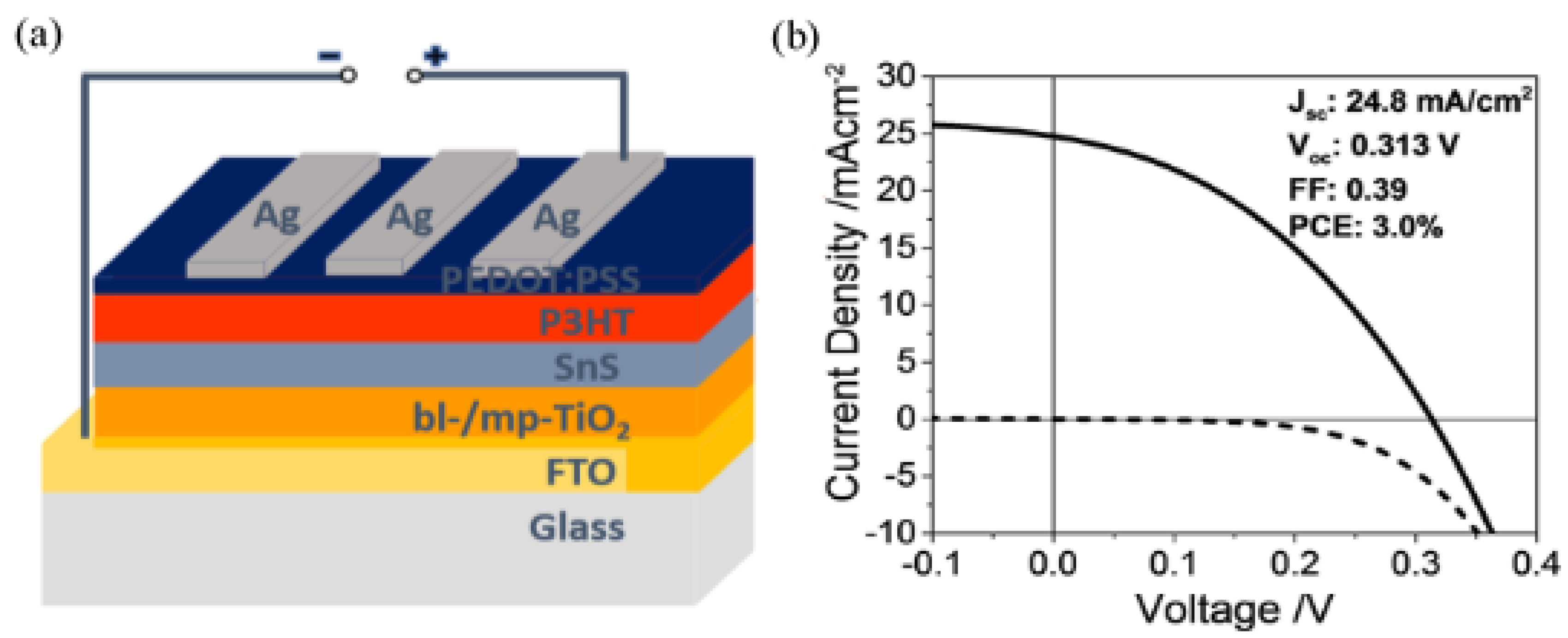
4. Applications of Bulk SnS

Tin(II) sulfide is a promising material for absorber layers in thin film solar cells. Noguchi et al. developed one of the first solar cells with a significant power conversion efficiency based on evaporation of SnS into an indium doped tin oxide (ITO)/n-CdS/p-SnS/Ag heterostructure. The cell had a short circuit current of 7 mA cm−2, an open circuit voltage of 0.12 V, a fill factor of 0.35, and a conversion efficiency of 0.29% [6].
Sinsermsuksakul et al. have reported the record-high efficiency 4.36% of p-type SnS-based solar cells, where an n-type zinc oxysulfide, Zn(O,S) layer has been combined with SnS, which acts as a hole blocking layer and favours electron transport. The major losses present in a typical SnS/ZnO cell are: losses from recombination at SnS grain boundaries and recombination at the SnS/ZnO(S) interface where both act as defects. A low open circuit voltage is the main limitation to obtaining a high conversion efficiency, with open-circuit voltage being dependant on the quantity of recombination pathways with a low open-circuit voltage suggesting a greater quantity of defects [8]. Solution-processed SnS cells made from quantum dots may have far lower efficiencies, with values of 0.008–0.066% due to the increased number of grain boundaries and recombination losses [20]. To reduce recombination and obtain highly efficient (4.36%) devices, multiple strategies have been applied, for example: (i) annealing of the SnS layer under a H2S environment to form larger grains with fewer grain boundaries; (ii) SnO2 of several monolayer thickness has been inserted between the p-SnS/n-Zn(O,S) junction; and finally, (iii) adjusting the conduction band offset by tuning the composition of the Zn(O,S) [8].
In Table 4, Steinmann et al. used commercially available SnS powder to produce phase-pure SnS films using a congruent thermal evaporation unit under high vacuum. Before film deposition, the commercially available SnS powder was pre-annealed in a separate furnace at 500 °C for 1 h. After this deposition method, thermally evaporated SnS film absorber layers in SnS-based solar cells achieved a National Renewable Energy Laboratory (NREL) certified efficiency of 3.88% [69]. Park et al. reported devices with efficiencies of up to 2.9% through an improvement in the morphology via annealing of the SnS layers deposited using pulsed-chemical vapour deposition using N2,N3-di-tert-butyl-butane-2,3-diamido-tin(II) precursors. Optimising the oxygen and sulfur content of Zn(O,S) helps in tuning the conduction band offset (CBO) at the p–n junction interface [70].
SnS has been used as a counter electrode (CE) in iodide/triiodide (I/I3)-based liquid junction dye-sensitised solar cells (DSSCs), as an alternative to expensive platinum (Pt). Chen et al. synthesised SnS nanosheets via the thermal decomposition of tin diethyldithiocarbamate and Na-DEDTC molecular precursors, with SnS applied as a CE in DSSCs. Excellent catalytic activity for triiodide reduction, resulting in a power conversion efficiency of 6.56%, is reported. Alam et al. [9] reported stoichiometric SnS nanostructured films deposited using a continuous spray pyrolysis (CoSP) technique with an aqueous spray solution of tin chloride and thiourea, with the film used as a CE in DSSCs as a replacement for Pt [10]. DSSCs have attracted a significant degree of interest, however they suffer from encapsulation issues due to solvent leakage of the liquid-based electrolyte. Another third-generation solar cell technology, i.e., inorganic–organic hybrid solar cells, are adopted from DSSCs; in these systems, inorganic semiconductor materials are used as sensitizers and low bandgap polymers act as hole transport materials. Guo et al. have shown all solid state inorganic–organic heterojunction solar cells with the structure: FTO/TiO2/SnS/P3HT/Ag, where SnS was deposited using chemical bath deposition (CBD) as a sensitizer and P3HT working as both a hole transporter and electron donor. An efficiency of 2.8% was achieved, with a high VOC of 0.85 V obtained. Haque et al. [71] have reported hybrid solar cells with ITO/TiO2/SnS/P3HT/MoO3/Ag architecture, where SnS was deposited by spin coating, using SnCl2 and thioacetamide (TAA) in pyridine as the tin and sulfur sources, respectively. The SnS layer was infiltrated with a P3HT solution left for 30 s on top of the SnS layer before spin coating. The device was completed via the thermal evaporation of MoO3 and Ag on top of the SnS/P3HT layers. An efficiency of 1.2% was obtained for solar cells produced via this preparation method [72]. In another study, Haque et al. have fabricated SnS thin film solar cells with glass/FTO/planar-TiO2/mp-TiO2/SnS/P3HT/PEDOT:PSS/Ag architecture that incorporated mesoporous TiO2/SnS/P3HT heterojunctions. The SnS layer was deposited using an environmentally friendly solution-based spin coating. The film morphology and surface coverage obtained could be tuned by modifying the precursor solution composition and deposition conditions. The PEDOT:PSS layer was inserted between P3HT layer and the Ag electrode to improve the VOC and JSC of the devices, which also enables efficient hole extraction while protecting the organic material during the metal contact evaporation. This leads to an increase in the power conversion efficiency from 2.6% to 3.0%. It is believed that highly efficient and more stable devices could be produced by further optimisation of the SnS film morphology, as well as through device engineering (Figure 4) [5].
Bulk SnS has also been used widely for thermoelectric energy generation via the Seebeck effect. Wang et al. have synthesised SnS via a chemical precipitation method. This method involved the reaction of a solution of SnCl2, ethylenediaminetetraacetic acid (EDTA), and triethanolamine [73] with a solution of sodium hyposulfide (Na2S2O3) dissolved in deionised water and ammonia. Annealing of the microstructure was found to change the SnS from the orthorhombic α-phase to the tetragonal β-phase at 858 K. A ZT value of 0.52 for polycrystalline SnS with no intentional doping at 873 K was obtained by Tang et al. [74] A ZT value of 1.6 at 823 K was obtained by Tan et al. from mechanically alloyed, spark plasma sintered SnS. This enhancement was obtained predominantly by tuning carrier concentration via doping; stoichiometric ratios and sintering temperatures had a less significant effect [29].
A ZT value of 0.41 for bulk SnS was obtained by Wang et al. at 848 K. A large Seebeck coefficient of 403 µv K−1 was observed at 848 K parallel to the pressing direction. The Seebeck coefficient was found to be double that prepared by mechanical alloying [75]. SnS for thermoelectric applications was also prepared via Asfandiyar et al. via a mechanical alloying and spark plasma synthesis method. A Seebeck coefficient of 352 µv K−1 was obtained at 232 K along two directions [30]. A hydrothermal synthesis method developed by Feng et al. has also been used to create bulk SnS for thermoelectric applications. The Seebeck coefficient was between 300 to 200 µv K−1 across 300 K to just over 700 K, with a distinct change around 350–500 K [76]. ZT values determined by a relaxation-time formalism-based theoretical model obtained by Gupta et al. was also found to match well to experimental values [77].

5. Transition from Bulk to Nanoscale

Two-dimensional (2D) materials are crystalline nanomaterials that generally exhibit two macroscopic or mesoscopic dimensions with a third dimension that can be as thin as one atom thick. They typically exhibit drastically different properties compared to their bulk counterparts from which they are derived due to confinement of their electronic states to within the two dimensions. Notable examples include the electric field effect in graphene [78] and the increase in band gap energy and/or nature (e.g., direct, indirect) in a range of layered semiconductors [79,80,81]. Due to its orthorhombic layered structure, the weak van der Waals forces between crystalline layers of SnS also allow exfoliation of this material into the 2D limit (Figure 5).
An increase in band gap from bulk to a few layers has been found to occur in a wide range of nanomaterials due to quantum confinement [80,81,83]. Quantum confinement effects in SnS occur at 14 nm, which is approximately twice the exciton Bohr radius for this material [29,84]. Ab initio simulations of these effects in the main group chalcogenides and black phosphorus have been reported by Gomez et al. using the Heyd–Scuseria–Ernzerhof Vienna ab initio simulation package (HSE VASP). The band gap energy of SnS was calculated to change from 1.20 eV (1033 nm, NIR) for the bulk to 1.60 eV (775 nm, far red visible) for bilayer SnS and was predicted to be as high as 1.96 eV for monolayer SnS (632 nm, red/orange vis), which means that the band gap energies of nanostructured SnS can potentially span a wide range of energies across the Vis–NIR region of the electromagnetic spectrum [1]. Note, however, that DFT simulations tend to underestimate these energy gaps, which can be seen in the discrepancy for the calculated bulk values. A similar band gap value for the monolayer at 2.09 eV was reported by Zhang et al. using HSE VASP simulation methods [85]. SnS remains an indirect band gap from bulk to monolayer as opposed to similar monochalcogenides such as GeSe and SnSe, which appear to transform to a direct band gap at the monolayer [81]. Other calculations of band gap from DFT performed by Georgios et al. have obtained band gap values of 2.72 eV, 1.57 eV and 1.07 eV for monolayer, bilayer, and bulk, respectively (Table 5) [28]. A change in band gap was found to be present for both orthorhombic α- and β-SnS simulated films with (100), (010) and (001) surfaces [86]. A combined experimental and computational study by Lewis and Seifert used a density functional theory tight binding (DFTB) model to predict a band gap energy between 1.6 and 1.7 eV for bilayer SnS, and compared these values to experimentally purified few-layer and bilayer SnS, the latter being the first example of exfoliation of SnS to the near-2D limit by a top-down process [1]. The density of states (DOS) and optical band gaps predicted by the quantum chemical simulations corresponded well with the experimental data. The study paved the way for many more studies of two dimensional IV–VI semiconductors.
In Figure 6, calculations of optimised lattice vectors for monolayer SnS performed by Gomez et al. using HSE VASP gave results: a = 4.44 Å, b = 4.15 Å and c = 11.5 Å [80], similar to previous work performed by Gashimzad et al. which showed a = 4.334 Å, b = 3.987 Å and c = 10.181 Å [87]. Zhang et al. have showed via DFT methods that monolayer SnS has the space group pmn21 with a = 4.05 Å and b = 4.34 Å, similar to experimental values which showed a and b to be 3.99 Å and 4.34 Å, respectively [85]. Experimental analyses of layer thicknesses have found a potential SnS monolayer thickness of 7 Å obtained by Higashitarumizu et al. [88]. Bilayer exfoliated SnS has a thickness of 11 Å [89], matching well to crystallographic data which give a value of 11.8 Å [82], and structural models giving a value of 11.2 Å for the bilayer which corresponds to the 8-atom unit cell [28]. The Brillouin zone has also been determined [90,91]. Density functional theory calculations by Dewandre et al. predict that interlayer spacing increases with decreasing layer number [92]. It was found that the a/b ratio moves to 1 as the 2D limit is approached; the Raman and reflectivity properties are also affected by thickness. It was also determined that the dielectric constant increases with the layer number [92]. Liquid-phase exfoliation and centrifugation of SnS has shown that because the SnS nanosheets are thinned and separated, a band gap of 1.65 eV is obtained, matching well with the HSE VASP calculations [1].
A theoretical study using first principle calculations with density functional theory (DFT) was conducted by Tritsaris et al. to determine the optoelectronic properties of single layer, double layer, and bulk SnS. It was found that the optoelectronic properties of SnS vary significantly with respect to the number of layers and the separation between them: the calculated band gaps were found to be 2.72 eV, 1.57 eV, and 1.07 eV for single layer, double layer, and bulk SnS, respectively, with values increasing with tensile strain along the layer stacking direction [28]. The minimum direct band gap was 2.72 eV, located at Γ (along the Γ–Y and Γ–Z directions the direct band gaps were 2.93 eV and 2.77 eV, respectively). These large band gaps suggest that single layer SnS is transparent for the longer wavelengths in the visible region of the electromagnetic spectrum. The electron effective masses were found to reduce as the number of layers increased from single to double layer to bulk. Tensile strain also increases electron effective mass for double layer and bulk SnS [28]. Figure 7 shows the odd–even quantum confinement effects for SnS at different layer thicknesses.

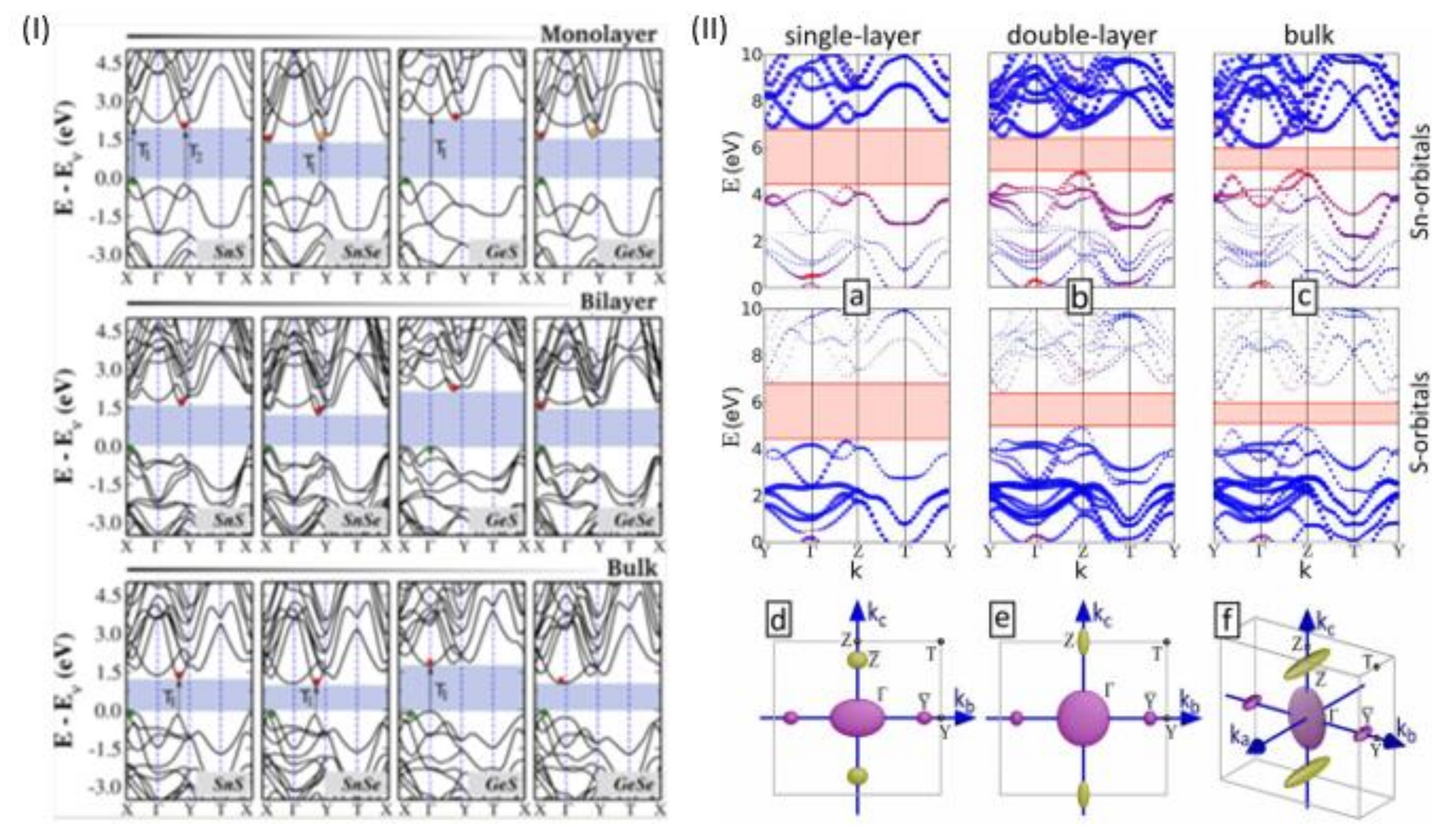
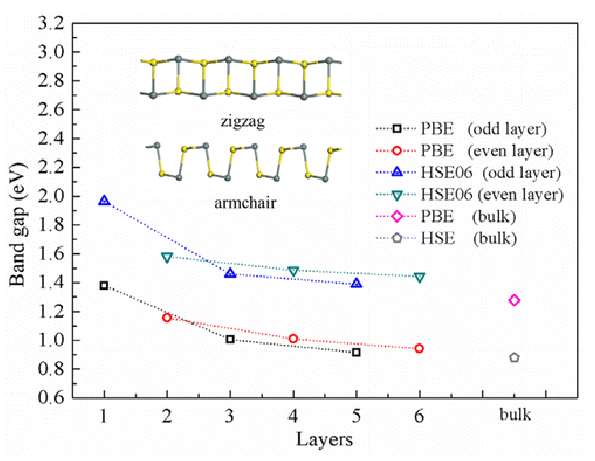
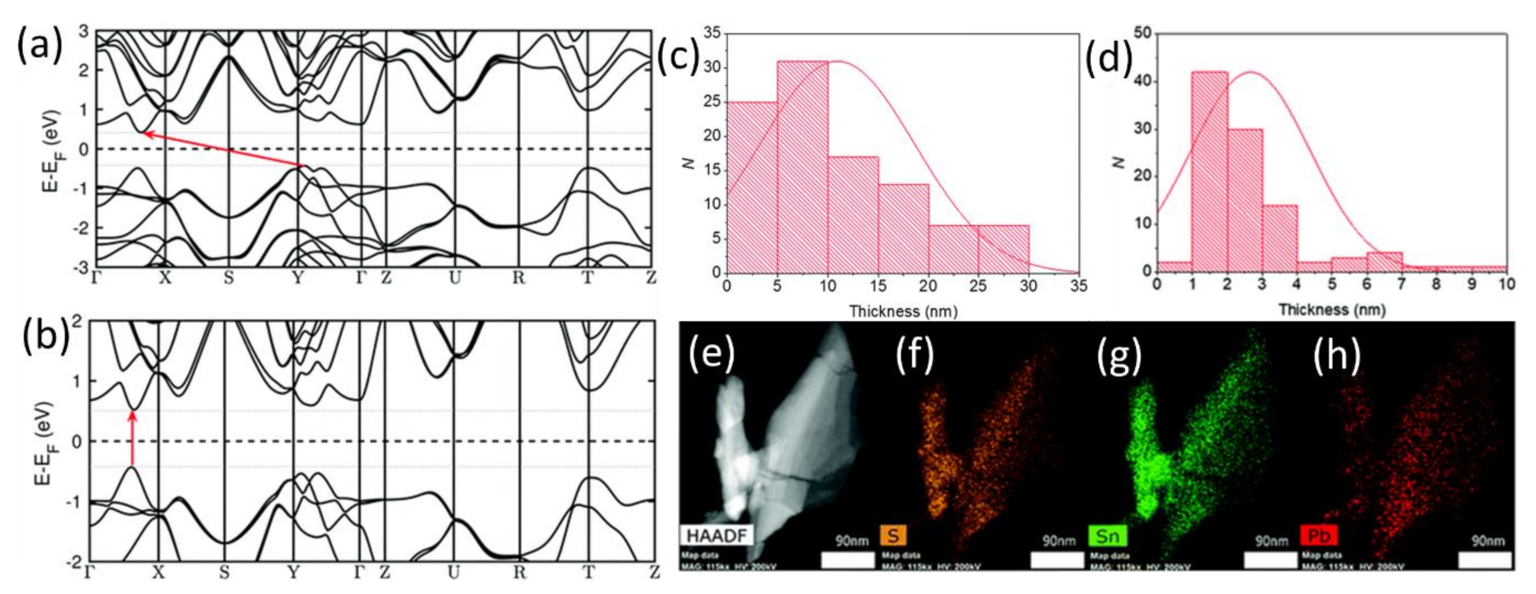
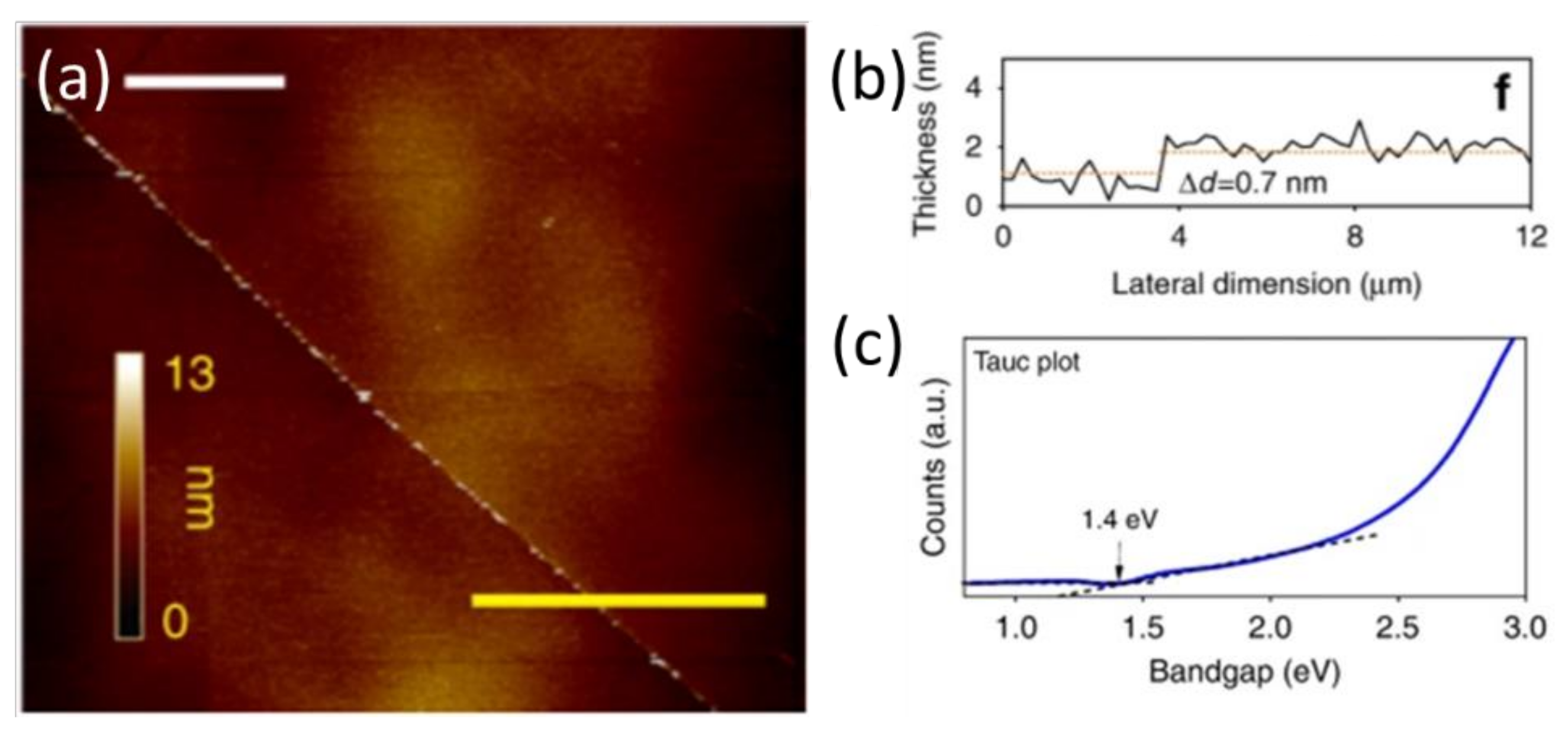
6. Properties of Two-Dimensional Tin(II) Sulfide

Two-dimensional SnS properties have been determined by numerous groups via experimental and computational methods, showing a range of intriguing properties compared to the bulk. Due to the anisotropic properties of SnS 2D crystals, different values for mobility are obtained, with the zigzag direction (20 cm2 V−1 s−1) having a mobility over 1.7-fold greater than that of the armchair direction as determined by Tian et al. [94]. Tin(II) sulfide monolayers have been found to have a high carrier mobility (10,000 cm2 V−1 s−1 to 38,000 cm2 V−1 s−1 for the monolayer along the a direction) [93] compared to 300 cm2 V−1 s−1 to 1000 cm2 V−1 s−1 for monolayer black phosphorous along the x direction [95].
Two-dimensional SnS has been determined to have nonlinear optical properties with a saturable absorption response. The strong coulomb interactions give rise to exciton enhanced annihilation (EEA) (rate 4.34 × 10⁻⁴ cm2 s−1). The quasiparticle interaction was determined by femtosecond transient absorption by Sarkar et al. [89]. Using a computational approach, Sandonas et al. have successfully determined the thermoelectrical properties of SnS monolayers. It was found that monolayer SnS has high levels of thermal anisotropy as well as a high thermoelectric figure of merit in both directions (ZTac = 4.5 and ZTZZ = 2.9 at 800 K) [96]. This was found to be higher than materials such as phosphorene (0.22) [97] and arsenene (0.8) [98], as well as bulk SnS (0.4) [75], (0.16) [29], (0.52) [74]. Thicker (100 nm) SnS nanobelts have already been successfully used as thermoelectric materials by Cheng et al. [99]. Tailoring of nanoscale SnS has also been performed by Yang et al., utilising doping with Na and Ag [100].
For applications in devices, a high level of stability is required to ensure a long lifetime. Two-dimensional SnS has been found to remain stable under harsh conditions such as in acids and electrolytes, as well as exhibiting long term cycling stability [94]. This makes it particularly useful compared to similarly structured semiconductors such as black phosphorous [101] and germanium(II) sulfide, which require anhydrous/anaerobic environments [102]. Calculations on SnS performed by Xin et al. have established the thermal and dynamic stabilities for both monolayer and bilayer via the use of VASP and PBEsol DFT [93].

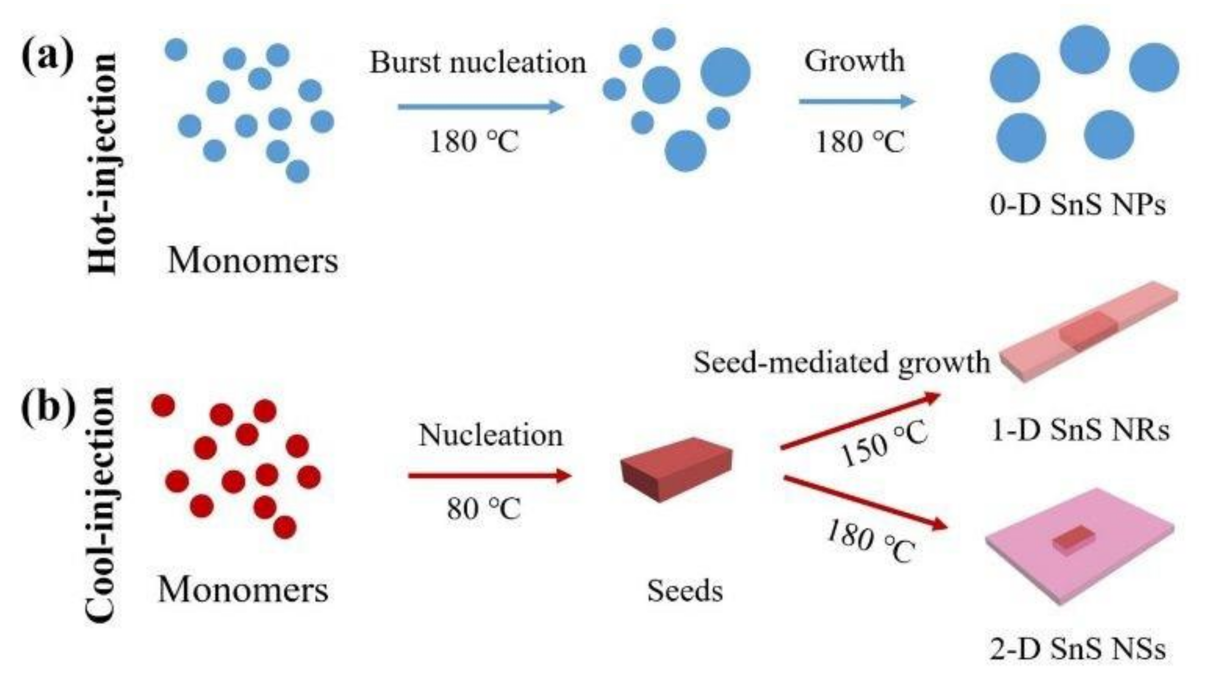
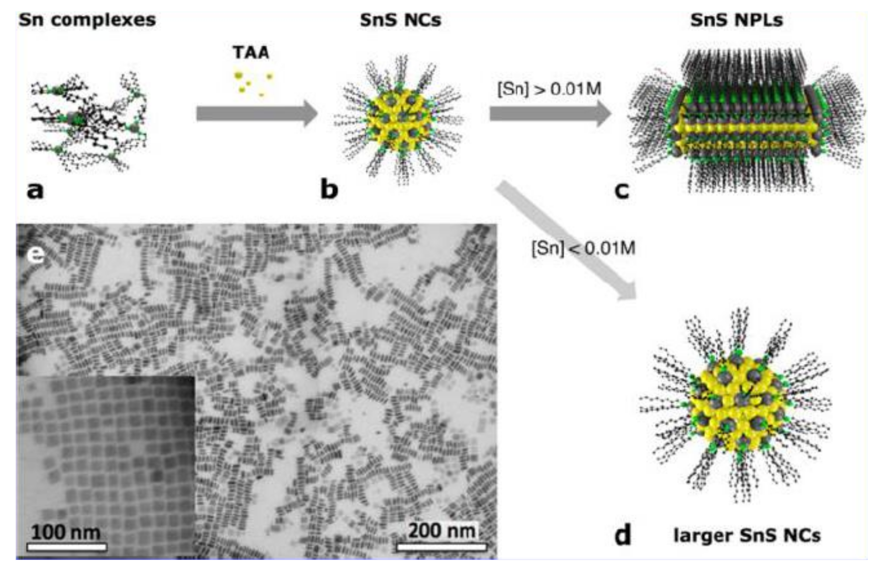
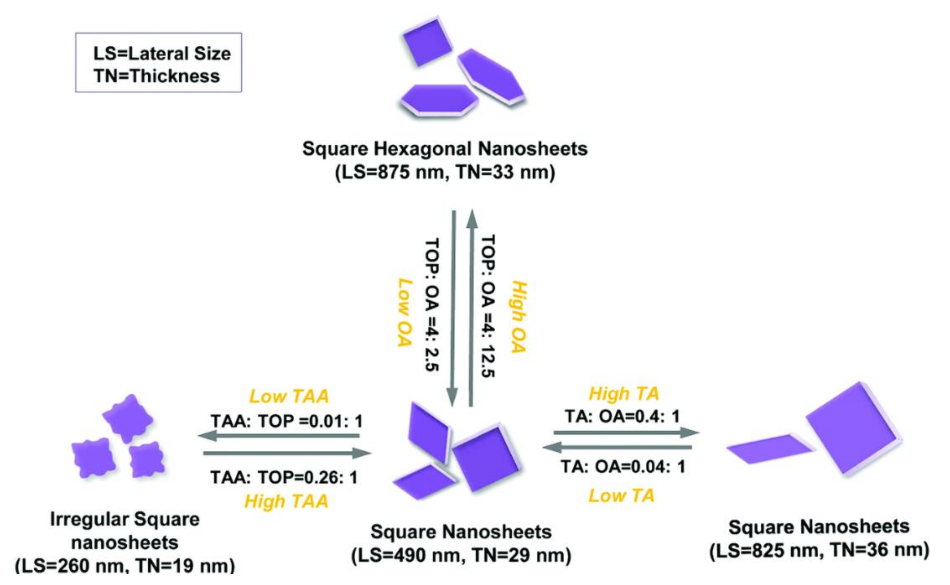
7. Synthesis of Two-Dimensional SnS

A range of methods have been developed for the creation of nanoscale SnS, ranging from liquid-phase chemical synthesis methods using a variety of different chemicals and reaction conditions including hydrothermal, solvothermal, aqueous solution and hot injection methods. Physical and chemical vapour deposition methods are also used for nanoscale SnS production as well as exfoliation directly from bulk SnS using mechanical and liquid-phase processes with a variety of solvents including N-methyl pyrrolidone (NMP), acetone, and isopropanol, among others.
The two broad methods of synthesis for nanomaterials are top-down and bottom-up methods. Top-down methods involve the breaking down of bulk material into nanoscale materials via liquid-phase and mechanical exfoliation. Bottom-up methods involve the direct synthesis of nanomaterials, which includes methods such as chemical and physical vapour deposition as well as wet chemical synthesis methods. Tin(II) and tin(IV) chloride (SnCl2 and SnCl4) are commonly used as reagents for the synthesis of nanoscale SnS, appearing in several published methods [73,103].
Few-layer SnS was first produced from bulk SnS via liquid-phase exfoliation by Brent et al. (Figure 8) [1] Liquid-phase exfoliation has significant advantages, such as being directly processable from solution, allowing rapid device fabrication as well as scalability, as shown for other materials such as graphene with a 100 litre scale being obtained, and production rates of 5.3 g h−1 [104], although it has several disadvantages, the main ones typically being the small sheet size and low monolayer yield [105]. Brent et al. exfoliated bulk SnS for 24 h in NMP in an ultrasonic bath followed by centrifugation at 180 × g (centrifugal g force) and then 11,620× g. Two-dimensional SnS nanosheets with an average thickness of 4.1 nm (corresponding to 3–4 bilayers) and a corresponding band gap value of 1.65 eV were obtained [1]. The lateral sizes obtained were between 50 and 100 nm, the larger lateral size due to the weak interlayer bonds relative to the in-plane bonds. The small number of sheets inspected by lattice resolution HAADF STEM imaging appeared to be mostly free from defects. SnS nanosheets from liquid-phase exfoliation have a high aspect ratio (proportional relationship of lateral dimensions) of lateral nanosheet length: lateral width due to anisotropy in the a–b plane, enabling the covalent bonds within the SnS layers to be preferentially broken perpendicular to the weaker zigzag direction [1].
Further separation and isolation of different band gaps has been obtained by Huang et al. via exfoliation in NMP and further centrifugation steps in a liquid-phase cascade centrifugation method. SnS was first ground in a pestle and mortar followed by the addition of NMP and probe sonication at 200 W for 4 s on/4 s off cycles for 8 h under an argon atmosphere. This was then bath-sonicated at 400 W for 48 h. SnS was then centrifuged at speeds of 2000–4000 rpm, 4000–6000 rpm and 6000–8000 rpm, respectively. The SnS produced had band gap values of 1.32 eV, 1.59 eV, and 1.71 eV, corresponding to average nanosheet thicknesses of 45.9 nm, 22.7 nm, and 6.1 nm, respectively [106].
Lead (Pb)-doped SnS nanosheets with the formula Pb0.2Sn0.8S were synthesised by the dithiocarbamate melt reaction of [Pb(S2(Net2)2] with [Sn(S2(Net2)2nBu2] at 450 °C under argon, the products of which were then exfoliated using NMP and separated by centrifugation at 180× g and 11,620× g by Norton et al. HAADF STEM and EDX of nanosheets showed an even distribution of Sn, Pb and S across the crystalline flakes, suggesting successful alloying at the nanoscale. Before high-speed centrifugation, the nanosheets had a length of 134 ± 45 nm and a thickness of 10.9 ± 7.7 nm. The highly centrifuged sheets had a lateral size of the order of tens of nm with a thickness of 2.7 ± 1.7 nm (Figure 9) [67]. The nanosheets obtained had direct band gaps of 1.25 eV and 1.86 eV, respectively, as determined by UV–Vis spectroscopy, which is striking because it meant that the addition of lead changes the indirect band gap of 2D SnS to a direct band gap in (Pb,Sn)S. DFT calculations showed that this was a consequence of strain on the SnS lattice introduced by the Pb ions that altered the electronic band structure of the material. The latter is a significant result, because it showed that by simple alloying of an isovalent element an indirect to direct transition could be garnered in SnS, which is an important feature for a material to be used in thin film optoeletronic devices; it typically increases absorption of light because there is no requirement for an accompanying change in crystal momentum. Traditionally, in materials such as transition metal dichalcogenides, this indirect to direct transition had to be elicited by thinning the material to a true monolayer, which is extremely low-yielding for 2D materials produced by liquid-phase exfoliation, and too time-consuming to be produced in bulk from micromechanical exfoliation. The approach has yet to be reported in other IV–VI semiconductors.
Alternative solvents have been utilised for the exfoliation of SnS nanosheets. Xie et al. have successfully exfoliated SnS nanosheets in isopropanol, which has the advantage of a low boiling point, hence being easier to remove. The nanosheets obtained were of an irregular size and shape, with lateral size of 50 nm and a thickness of 6 nm. The nanosheets were found to be stable in solution over a period of 30 days, as determined by UV–Vis spectroscopy [107].
Sarkar et al. have reported the use of acetone to successfully exfoliate SnS. The SnS was bath-sonicated for 20 h at 100 W and 40 kHz under a nitrogen environment followed by nanosheet separation via 15 min of centrifugation at 8000 rpm. The nanosheets obtained had an average thickness of 1.1 nm, with all nanosheets being between 0.8 and 1.5 nm thick, indicating that all sheets were only several monolayers in thickness, with the 0.8 nm sheet being close to SnS monolayer thickness (0.7 nm) [108]; selected-area electron diffraction (SAED) patterns confirmed that the nanosheets were single crystalline at the clear rhombus-like lattice fringes. The Ag Raman mode was found to shift by 3.46 cm−1, which was attributed to the evolution of coupling between electronic transitions and photons [89]. Further work performed by Sarkar et al. suggests that other solvents that can disperse SnS include dimethyl formamide (DMF), ethanol, dimethyl sulfoxide (DMSO), and methanol; as determined by UV–Vis and Raman, the size of the nanosheets produced and further characterisation was not obtained [109].
The effectiveness of nanomaterial exfoliation and dispersal is dependent on the Hansen solubility parameters: δd, δP and δh, which correspond to the dispersion forces, the polar forces, and the hydrogen bonding forces between molecules, respectively. From these parameters, it can be determined whether a material will dissolve or disperse. The Hansen parameters for the solvents NMP, IPA and acetone are listed alongside those of SnS in Table 6.
Potential future work could be focused on liquid-phase exfoliated SnS via aqueous surfactant solutions, eliminating the need for volatile, toxic, or costly solvents. This has been shown to work with materials such as black phosphorous. The exfoliation method utilised deoxygenated water and sodium dodecyl sulfide (SDS) to produce nanosheets with thicknesses under 10 nm [111].
An alternative top-down method is mechanical exfoliation, which can be used to produce nanosheets with a significant lateral size relative to thickness. This method has been used since the discovery of graphene [79] to produce high quality 2D materials, although lacks scalability. Relatively large flakes of SnS were created by Higashitarumizu et al. via the use of micromechanical exfoliation from bulk SnS using tape and Au exfoliation. The nanosheets obtained were found to be 13.8 nm, 10.5 nm, and 4.3 nm in thickness with a lateral size over several µm, which is up to several orders of magnitude larger than those obtained from liquid-phase exfoliated few-layer SnS [1,106]. Oxygen annealing was then used to successfully thin the flakes down to close to monolayer thickness [88]. A comparison of tape and Au mediated exfoliation has been performed by Higashitarumizu et al. This showed that tape exfoliated SnS was found to have a lateral size of several µm with a thickness in the range of tens of nm. Au exfoliated nanosheets were found to have a larger lateral size (tens of µm) with thicknesses showing a wide distribution down to 1.1 nm. The increased lateral size for Au mediated exfoliation was attributed to the strong, semi covalent bonding between Au and S atoms. The produced Au exfoliated SnS had a thin SnOx layer, making it ideal for the creation of thin SnS/SnOx heterostructures, but ineffective for creating large area, pure SnS nanosheets [112].
SnS has been successfully separated into nanosheets via the use of lithium intercalation by Ju et al. SnS was synthesised via the heating of Sn and S in a quartz ampoule at 950 °C for 6 h. Intercalation was undertaken via the addition of ethylene glycol and lithium hydroxide with heating in an autoclave at 200 °C for 48 h. The nanosheets were then added to aqueous tartaric acid and heated in an autoclave for 203 °C for 2 h to form porous SnS nanosheets. Finally, the polyaniline was synthesised around porous SnS to form the composite. The SnS produced was from 200 nm to 500 nm in lateral size. It was found via field effect TEM (FETEM) that the microhardness of the nanosheets changes from pristine (80 kgf mm−2) to porous (70 kgf mm−2). The nanosheet composite formed had a ZT value which increased with temperature up to 0.078 at 177 °C, which was 458-fold higher than the pristine nanosheet SnS [113].
Chemical synthesis is a versatile method of creating nanoscale materials, which has advantages of versatility of reactants and conditions, enabling a range of morphologies to be produced. However, in some cases dangerous reactants and conditions such as high temperatures may pose a risk. Chemical synthesis may also carry the risk of unwanted products and may require purification. Commonly, tin chloride is used as the source of Sn [103]. Zhu et al. have developed a novel hydrothermal synthesis method to produce 2D single crystalline nanosheets with micron scale lateral sizes. The reaction was undertaken via the use of SnCl2.H2O, thioglycolic acid (TGA) and Na2S heated in an autoclave at 200 °C for 48 h with different morphologies obtained from changing the Sn/S ratio. Nanosheets up to micron scale were produced with TEM showing a 2D morphology. It was determined via XRD that SnS grows preferentially perpendicular to the (111) direction. The inclusion of TGA prevented nanosheets from aggregating, allowing improved control over nucleation and growth. The formation of the initial SnS nuclei for nanocrystal growth came from the reaction: SnCl2 + Na2S → SnS + 2NaCl [103].
The hydrothermal method has also been used by Tian et al. to produce microbelts with a thickness of 700 nm and a length of 15 µm. The microbelts were synthesised using SnCl2.2H2O in distilled water and thiourea in an autoclave at 200 °C for 24 h. The microbelts produced were then utilised as photodetectors [114]. Hydrothermal synthesis requires the use of consistent high temperature over a long period, however is capable of producing high quality, single crystalline nanomaterials with the possibility of bridging the gap between bulk and 2D SnS with the possibility of creating high quality microstructures.
A film consisting of 2D nanobelts of SnS with a thickness of 20–30 nm with lengths 3–5 µm length and widths ranging from 300–400 nm was produced by Cao et al. via a simple chemical bath deposition. SnCl2.2H2O and thioacetamide (TAA) in distilled water were reacted together for 1–2 h at 80 °C, and sulfuric acid was used to keep pH between 0.4–1.0. The reaction occurs by the release of Sn2+ and S2− ions, which are obtained by the dissolution of Sn salt and decomposition of TAA, respectively. This step is followed by condensation of the ions onto substrates. Similarly, this method also relies on nucleation and growth steps. Phase-pure, single crystalline SnS was formed with morphology changing depending on pH and TAA concentration. A greater concentration of TAA leads to the creation of a more compact film due to the increased S2− concentration. Higher pH led to the creation of thinner, looser nanobelts due to decreased S2− release and increased precipitation of Sn(OH)2. The SnS produced had a band gap of 1.41 eV and 1.39 eV for 1 h and 2 h deposition, respectively, as determined by Tauc plots from UV–Vis [115].
Thin films consisting of SnS nanosheets have been synthesised by Jing et al. with individual sheet thicknesses of 200–400 nm. The SnS was synthesised by the reaction of SnCl2.2H2O and thioacetamide at a pH range of 0.2–1.5, which was adjusted using sulfuric acid. The reaction was undertaken at 120–180 min at 80 °C. Sheet-like morphologies were obtained from pH 0.2–0.7 with film thicknesses of 4.37 µm, 4.03 µm, and 2.14 µm for pH 0.2, 0.4, and 0.7, respectively. Thinner films are produced at higher pH due to the precipitation of Sn(OH)2 [116]. The SnS is produced by the release and reaction of Sn2+ and S2− ions, similar to the reaction undertaken by Cao et al. [115]. The SnS was used in the creation of an FTO/SnS/CdS/Pt photocathode.
Shan et al. have synthesised SnS nanosheets with large lateral sizes of 5 µm to 20 µm and thicknesses of 100 nm with no impurities. The reaction involved the addition of octadecene into an aqueous SnCl4.5H2O solution in a three-necked flask. This was degassed and heated to 130 °C before being heated to 280 °C, followed by the addition of S in oleylamine, and was then maintained at 280 °C for 30 min. This was then centrifuged and purified via washing in ethanol and cyclohexane. The SnS produced was used for ethanol sensing [117]. Choi et al. have synthesised SnS nanosheets for a reduced graphene oxide (rGO)–SnS composite. The SnS nanosheets were synthesised onto rGO prepared via the Hummers method. The rGO in ethanol dispersion had tin(II) acetate and thioacetamide added before stirring and sonication. The mixture was then added to an SUS 316 reactor and heated in a molten salt bath for 10 min at 400 °C. The samples were then cooled and washed. The bare SnS produced had a thickness of 100 nm with lateral sizes of 0.5–2 µm. Smaller, irregular nanosheets with lateral sizes around 100 nm were obtained for high precursor concentrations. The two sizes of SnS produced were due to the differing homogeneous and heterogeneous nucleation mechanisms. The smaller SnS produced by heterogenous nucleation occurred on the basal plane of graphene oxide, with the larger SnS nanosheets being produced in the fluid phase via homogeneous nucleation [118].
Hot injection synthesis methods are useful, because one can precisely control the size, shape, and composition by controlling synthesis conditions including reaction time and temperature, solvent, precursor types, and concentrations. The main parameters, which have to be controlled during nanocrystal synthesis, are size (emission colour), size dispersion (photoluminescence line width), and surface passivation (photoluminescence quantum yield, PLQY). Surface ligands play a very important role in tuning nanocrystal properties such as processability, reactivity, and stability. They also help to prevent nanocrystal agglomeration and facilitate the dispersion in a variety of solvents but deteriorate the performance of solar cells. Wu et al. have synthesised SnS nanocrystals of different dimensions (0D, 1D, and 2D) using a facile colloidal route and studied their photoelectrochemical performance. A hot-injection method was used to synthesise 0D SnS nanoparticles (NPs), whilst a temperature-controlled cool-injection method was used to fabricate 1D SnS nanorods (NRs) and 2D SnS NSs. It was found that the order of injection of 1-Dodecanethiol (DDT) and thioacetamide is crucial to control the dimension of SnS nanocrystals. In the cool-injected method, the pre-injected thioacetamide not only served as a S source to form SnS seeds, but also coordinates to the tin centre to form Sn(I18hioimidateate, favouring the anisotropic growth of SnS NRs and NSs (Figure 10) [119]. Biacchi et al. have reported the colloidal synthesis of different shaped SnS compounds, including nanosheets, and studied their photocatalytic degradation behaviour with methylene blue (MB). In-depth crystallographic analysis was performed on as-obtained SnS systems. For nanosheet synthesis, tin acetate, oleylamine, and sulfur were used with the reaction occurring in a three-necked flask at 180 °C. The nanosheets produced were of the order of 270 nm lateral size. Kubelka–Munck functions determined the SnS nanosheets to have an indirect and direct band gap of 1.1 eV and 1.3 eV, respectively [120].
Kergommeaux et al. have reported a new synthetic method for the synthesis of well-calibrated square SnS nanoplatelets showing comparable small dimensions—thickness 4–15 nm and edge length 15–100 nm—where oleylamine, trioctylphosphine and oleic acid are used as ligands. A long-term colloidal stability (several years in chloroform) was observed. Stability is a prerequisite for nanoparticle processing into thin films or for use as an additive to polymer matrices (Figure 11) [121].
Li et al. have also prepared SnS nanosheets using trioctylphosphine and oleic acid as ligands. Tin(II) acetate (TA), oleic acid (OA) and trioctylphosphine (TOP) were dissolved in diphenyl ether (DPE) and the mixture was heated to 230 °C under nitrogen. Thioacetamide in dimethylformamide was then added and left to react for 5 min before cooling, centrifugation, and redispersion in toluene. DFT (CP2K package) was also performed to determine the formation mechanisms using the PADE LDA functional, a DZVP basis set, GTH-PADE potential with a SnS nanocrystal consisting of 224 Sn and 224 S atoms.
For the synthesis of square-like SnS nanosheets, TA was partly transformed to tin oleate. The synthesis of nanosheets begins with complexation of the tin precursor and OA followed by the synthesis of SnS nanocrystals via the reaction of Sn and S precursors; the growth step then occurs via the SnS nanocrystals. Lowering the amount of TA was found to form larger, thicker nanosheets due to the reduced number of nuclei formed. When TOP is added without OA, small, square nanosheets and nanoparticles are formed, indicating that TOP enhances the formation of (101) square facet nanosheets. Increasing the OA concentration was found to increase both the size and thickness. For the synthesis of hexagonal nanosheets, OA concentration must be above a certain threshold (2 mmol). The formation of large laterally sized, hexagonal nanosheets is due to the large absorption energy of OA ligands on (100) facets as opposed to (101) and (010) (Figure 12) [122].
Aside from producing thicker, bulk SnS films such as those produced by Ahmet et al. [123], chemical vapour deposition (CVD) and other vapour deposition methods have been used to synthesise 2D and nanoscale SnS. CVD is an effective way to produce nanostructured SnS with a variety of morphologies and compositions, including composites. CVD also has the potential advantages of scalability. CVD can also utilise a range of chemical precursors and produce nanosheets of high quality. However, chemical vapour deposition often requires transfer between growth and transfer substrates, high temperatures, and carrier gases, as well as not being directly processable from solution [124].
Liu et al. have developed a CVD method involving the use of SnO and S powders in separate boats with an Ar carrier gas with the furnace heated at 650 °C. The S boat was moved to the centre of the heating zone when the temperature was stable. The SnS nanosheets produced were square faceted, horizontally aligned nanosheets with 25 nm thickness with lateral sizes of 2 µm; these nanosheets were used in photodetection [125]. Nanosheets have been produced via a similar method by Mutlu et al. SnO2 and S powders were evaporated onto a B-doped Si substrate at 550 °C under nitrogen within a tube furnace. The tube furnace had the temperature maintained for 40 min. The formation mechanism involved the initial evaporation of SnO2 at 400 °C and the formation of SnO2 clusters, which acted as SnS nucleation sites. At lower temperatures, the following reaction occurs: SnO2 (s) + 1.5 S2 (g) → SnS2 (s) + SO2 (g). At higher temperatures, the reaction: SnO2 (s) + S2 (g) → SnS (s) + SO2 (g) occurs. SnS was formed at 550 °C with SnS2 formed at 425 °C. The SnS produced was square faceted and horizontally aligned, with lateral sizes of over tens of µm with thicknesses of around 30 layers [126].
Price et al. have developed a method of chemical vapour deposition of nanoscale SnS films at a range of temperatures from 300 °C to 545 °C. The films were formed from a mixture of H2S and SnCl4 introduced into a nitrogen gas stream for 30 s and 3 min of deposition. A platelet structure was formed at 475 °C, with ovoid, needle-like and agglomerated structures at 300 °C, 525 °C, and 545 °C, respectively. The platelets formed had lateral dimensions of 800 nm by 800 nm with 25 nm thickness. At higher temperatures, SnS is produced as opposed to SnS2. The films obtained at 300 °C at 3 min deposition had greater dimensions (1000 nm × 500 nm) compared to 30 s deposition (500 nm × 100 nm) [48]. Physical vapour deposition was performed by Kawamoto et al. via the use of commercial and high purity SnS powders and nitrogen carrier gas onto freshly cleaved mica. The deposition temperatures were 410 °C, 440 °C, and 470 °C at 10 Pa pressure. The commercial SnS powder successfully formed a SnS monolayer with a thickness of 0.8 nm and a lateral size of µm scale. Submicron grains of Sn2S3 were observed for SnS produced from the commercial powder. The lateral growth of the SnS monolayer from impure SnS was believed to be facilitated by the enhanced surface distribution of SnS precursor molecules. The mechanism is believed to be due to evaporation of the S in Sn2S3 before SnS, facilitating the surface diffusion of the SnS precursor molecules [127]. Sutter et al. have also enhanced the lateral size of chemical vapour transport-deposited nanosheets via the addition of sulfur to high purity SnS, although no monolayer was formed. Without sulfur pre-exposure the thicknesses varied, with values up to 400 nm and an average lateral size of 3.5 µm. With sulfur pre-exposure, the lateral size reached up to 7.9 µm, with 30% of nanosheets having thicknesses under 50 nm. Thinner nanosheets (under 20 nm) have circular morphologies which transitioned to a square morphology as the thickness increased. The change in the proposed growth mechanism was that the additional sulfur leads to a transient surface passivation of SnS flakes during growth, reducing reactivity of the top facet and limiting vertical growth relative to the horizontal [128].
Xia et al. have also prepared SnS nanosheets via a physical vapour deposition method. The SnS was grown on mica substrates under 20–300 Torr pressure in high purity argon with the heating zone set to 600–800 °C. The SnS produced had lateral sizes of several µm with thicknesses ranging from 5.5 nm to 14.6 nm. The nanosheets produced were square, with the thinner nanosheets possessing comparatively rough edges and surfaces. An increase in temperature and pressure was found to increase the nanosheet dimensions up to 40 µm lateral size with thicknesses up to 230 nm [129]. Square SnS nanosheets grown via physical vapour deposition (PVD) have also been prepared by Yuan et al., with square nanosheets of lateral sizes of 7 µm and thicknesses of 12 nm produced. These nanosheets were prepared at 650 °C from 99% pure SnS and deposited onto mica. These nanosheets were then turned into photodetectors using a photolithographic-pattern-transfer (PPT) technique [130].
The ability to control the thicknesses and lateral size of SnS with PVD makes it an effective method for high quality SnS nanosheet synthesis—the ability to synthesise monolayer SnS is also a significant advantage. However, the morphology of the nanosheets appears limited, with most PVD producing square nanosheets or thinner, irregular, or circular shapes. Khan et al. have developed a method for growing high quality, wafer scale monolayer SnS via the reaction of H2S gas with molten tin. Elemental tin was melted at 350 °C onto a clean glass slide in a glove box environment consisting of 50 ppm H2S in nitrogen. A heated glass slide was then used to expose the molten Sn surface, and finally a Si/SiO2 (300 nm) substrate was touched onto the Sn droplet to exfoliate the monolayer SnS [108]. The SnS produced had a thickness of 0.7 nm, as determined by atomic force microscopy (AFM), with lateral sizes in the range of tens to hundreds of µm with no cracks and a consistent thickness. The SnS was found to possess a carrier mobility of 35 cm2 V−1 s−1 with a piezoelectric coefficient of 26 pm V−1. Piezoelectric nanogenerators were successfully formed from the monolayer SnS produced. This method appears to be the most effective for the synthesis of large area, monolayer SnS [108] (Figure 13).
Lower dimensional SnS has also been produced with 0D quantum dots produced by several groups with applications in solar cells and photovoltaics [131,132,133,134,135], degradation of organic dyes [136], and biomedical applications [137]. One-dimensional nanorods have also been produced by several groups [138,139,140,141,142], which have applications in hydrogen storage [143], lithium storage [144,145], solar cells [146], and field emission applications [147]. Other SnS structures including nanopyramids [148], nanoflowers [149], and nanospheres [150,151] have also been created by several groups. More detailed synthesis and property information of these materials is beyond the scope of this review.

8. Applications of Two-Dimensional Nanoscale SnS

Two-dimensional SnS has several applications; due to the band gap of thin layer SnS, many examples of photonic devices have been created via a variety of methods. Exfoliated nanoscale SnS has been used in the creation of tuneable bandgap photodetectors [106]. Physical vapour deposition of SnS of 42.6 nm thickness was found to exhibit differing responses for the armchair and zigzag directions. A photoresponsivity of 365 A W−1 was determined with an external quantum efficiency up to 9.92 × 10⁻⁴ [152]. SnS films of 15 nm thickness, formed by physical vapour deposition, have been used in photodetectors alongside Bi2Te3, showing a high responsivity (115 A W−1) and high quantum efficiency (3.9 × 10⁴%) [153].
Devices prepared by Huang et al. from 2D SnS have been found to remain stable under potentially harsh conditions, with the device remaining functional over six months in 0.1M Na2SO4 along with other conditions, including an acidic environment and with neutral electrolytes [106]. The devices consisted of cascade centrifuged SnS nanosheets on ITO-coated glass as the working electrode, platinum as the counter electrode, and a saturated calomel electrode as a reference electrode submerged in an electrolyte solution. Nanosheets separated between 2000–4000 rpm, 4000–6000 rpm, and 6000–8000 rpm (with corresponding band gaps of 1.32 eV, 1.59 eV, and 1.71 eV, respectively) were used in the electrodes, with aqueous H2SO4, NaOH and Na2SO4 used as the electrolytes. A maximum detectivity of 1.92 × 10⁸ Jones for 0.5 M Na2SO4 with SnS centrifuged between 4000–6000 rpm was obtained. A rise and recovery time of 0.1 s and 0.3 s, respectively, was obtained for this device with a photoresponse of 1590 nA cm−2. The high photoresponse of 4000–6000 rpm centrifuged nanosheets was due to the favourable optical absorption properties alongside the number of active sites present. The photoresponsivity was higher for the lower wavelength of 365 nm. The detectivities and responsivities are higher for the Na2SO4 electrolyte. The SnS was found to be more stable under acidic than basic conditions. DFT calculations suggested that this was due to the formation of Sn–O bonds, which leads to the lengthening of the Sn–S bonds, making them weaker. The nanosheet devices were found to have self-powered photoresponses, with voltage improving the current response [106].
Vertically grown 2D SnS has also been formed into a composite SnS/perovskite complex, providing a broadband response. The pure SnS device gave a 0.05 µA photocurrent at 365 nm and 4 mW cm−2; with addition of the CH3NH3PbI3 perovskite, the photocurrent increased to 7.1 µA. The rise and fall times for the composite device were 9 ms and 42 ms, respectively. It was determined that there was efficient charge transfer between the SnS and perovskite, as confirmed via time-correlated single photon counting [154].
Other examples of 2D SnS-based photodetectors have been created by colloidal synthesis; the devices produced by this method by Li et al. were found to have a detectivity of 4 × 10⁹ Jones, with a spectral response of 3 × 10³ AW−1 and a sensitivity of 0.95 as calculated by (Iill−Idark)/Idark. Fast transitions between light and dark were also observed. The nanosheets tested were between 24 nm and 29 nm thickness with lateral sizes between 150 nm and 500 nm [122].
SnS nanosheet film-based photodetectors of 15 nm thickness with Bi2Te3 electrodes prepared by Yao et al. had a response of 115 A W−1, a detectivity of 4.1 × 10¹¹ Jones, a quantum efficiency of 3.9 × 10⁴% with a band gap of 1.13 eV, and a rise and fall time of around 1 s and 2 s, respectively, was also obtained. The device was prepared on a polyethylene terephthalate substrate and was found to retain photoresponsivity over 100 bending cycles, indicating that SnS may be useful in flexible photodetectors and wearable devices [153].
Zhang et al. have successfully produced a SnS-based four-terminal device that can function along the zigzag and armchair planes of a SnS nanosheet. An 808 nm laser was used as the illumination source. It was found that the zigzag device had a faster rise and fall time (0.2 s, 0.2 s) compared to the armchair configuration (0.4 s, 0.4 s). Both the dark and light currents were higher for zigzag compared to armchair planes: 31.8 µA vs. 19.3 µA, respectively, for dark, and 54.2 µA vs. 36.4 µA, respectively, for light. The photoconductivity ratio (σzigzag/σarmchair) was 1.49. The differences are due to differences in the effective masses of carriers along the two directions. A similar, two-terminal device was found to exhibit a reduction in the photoconductivity ratio after oxygen plasma treatment to introduce defects. After 300 s of treatment, the anisotropic response was almost completely removed. Decoration with Au nanoparticles was found to increase photoresponsivity from 365 A W−1 to 635 A W−1 and quantum efficiency from 5.7 × 10⁴% to 9.92 × 10⁴% [152].
Photodetectors prepared by Yuan et al. via a physical vapour deposition method have been determined to have a responsivity of 1.6 × 10⁶ mA W−1, an external quantum efficiency of 2.34 × 10⁵%, a detectivity of 3.42 × 10¹¹ Jones, and rise and fall times of 7.6 ms and 29.9 ms, respectively. The responsivity was significantly higher than other SnS-based devices [130]. Shao et al. have prepared a SnS nanoribbon-based photodetector device via a polyol reflux method. The nanoribbons had thicknesses of 10–20 nm. A photocurrent density of 87 µA cm−2 was obtained under 1 sun illumination at 100 mW cm−2, alongside a rise and fall time of 0.1 s. Flexible photodetectors were successfully doctor-bladed onto polyethylene terephthalate (PET) substrates, allowing the creation of flexible SnS devices. The nanoribbons were found to have a higher photocurrent than nanoparticles prepared for a similar device [18].
As well as bulk SnS, 2D SnS has also been used in the formation of solar cells. Jamali-Sheini et al. have grown vertically aligned SnS nanosheets on clean glass substrates as well as those coated with Ag and Au buffer layers. Sheet thicknesses of 80 nm, 37 nm and 51 nm were found for the buffer free glass, Ag, and Au layers, respectively. A flat layer of SnS was formed on the Ag and Au buffer layers before the growth of the vertically aligned nanosheets. The growth method was believed to occur via the vapour liquid solid (VLS) route, where nanosheets have a droplet of metal or alloy which controls the diameter, growth, and orientation, with the droplets acting as active sites for growth. Absorption coefficients determined by UV–Vis were 37%, 90%, and 70%, for free coated SnS, Ag, and Au buffer layers, respectively, with corresponding band gaps of 1.5–1.6 eV, ≈1.4 eV, and ≈1.7 eV, respectively. The figures of merit for the Ag-coated device were: VOC: 0.36 V, JSC: 5.6 mA cm−2, fill factor: 0.48, PCE: 4.83%, Rss: 19 Ω cm−2, Rsh; 302 Ω cm−2; the efficiency was 0.97%, significantly higher than free-coated SnS (0.29%) (Figure 14) [155].
Two-dimensional SnS has also been successfully used as a counter electrode to improve efficiency in I3-/I dye sensitised solar cells. Chen et al. have prepared SnS hexagonal nanosheets with diameters 50–150 nm via the formation and decomposition of a tin diethyldithiocarbamate. The photovoltaic parameters obtained were: JSC: 17.7 mA cm−2, VOC: 740 mV, fill factor: 50%, Rs: 6.34 Ω, Rct: 0.94 Ω; the efficiency was 6.56%, which compared favourably to platinum (7.57%). The cyclic voltammetry profile showed a similar catalytic activity to platinum with a smaller peak to peak splitting (225 mV vs. 260 mV), indicating that SnS may be superior to Pt with regards to electrocatalytic activity and reversibility of the I3/I redox reaction [9]. Fewer dimensional SnS quantum dot sensitised mesoporous TiO2-based cells [156] and solution-processed SnS quantum dot solar cells have also been produced [157], as well as 1D SnS nanorod-based cells [158].
The nonlinear optical absorption coefficient of SnS (50.5 × 10⁻³ cm GW−1, an order of magnitude higher than black phosphorous) makes SnS a potentially effective material for ultrafast laser generation. Optical absorption peaks at 1180 nm and 1480 nm suggest that SnS nanosheets may be a promising optical material for the telecommunications band. Liquid-phase exfoliated nanosheets of SnS produced by Xie et al. have been found to have rapid response times of τ1 (short decay time) = 873 fs and τ2 (long decay time) = 98.9 fs. These times correspond to the electron thermalisation in the band and the recombination of the carriers, respectively. A pulse width of 656 fs was obtained. The rapid response times allow SnS to be used as a modulator in the GHz to THz range [107]. For comparison, black phosphorous lasers have been found to have a pulse width of 946 fs [159].
Due to the ability to successfully intercalate ions between the atomic layers, SnS has attracted significant interest in energy storage, with the large interlayer spacing allowing the intercalation of larger Na+ ions as well as smaller Li+ ions. SnS also has a lower volume expansion than SnS2 (242% vs. 324%), making it more suitable for repeated cycling [160]. Two-dimensional SnS has also been used successfully in the creation of a variety of energy storage devices, such as lithium-ion batteries, with nanosheets showing improved properties compared to bulk [161]. This is due partly to the increase in effective dielectric constants from around 15 for bulk to around 25–30 for monolayer SnS, as calculated from the DFT ab initio package by Dewandre et al. [92]. Batteries utilising SnS nanomaterials typically exhibit a reduction in discharge capacity due to the reaction: SnS + 2Li → Sn + Li2S [22,161,162]. Composites utilising 2D SnS show stable capacities of 595 mAg−1, 580 mAg−1 [22], 660 mAg−1 [163], and have been obtained by a variety of groups with the respective capacities maintained over tens [22,164] and even thousands of cycles [163]. Hybrid SnS/rGO nanosheets have been used by Li et al. for the creation of a lithium-ion battery hybrid anode. The composite showed improved performance due to the high capacity of SnS combined with the conductivity of graphene and the large surface area of nanomaterials; the SnS was found to be around 10–20 nm in thickness. The reversible capacity was determined to be 791 mAh g−1 with 595 mAh g−1 retained after 50 cycles at 100 mA g−1 (Figure 15) [164].
Hierarchical structures utilising nanoscale SnS allow for the potential improvement of lithium-ion storage devices [81]. SnS nanosphere composites with an inner 2D SnS layer have been prepared by Zhao et al. via a chemical synthesis method utilising SnCl2 over TiO2 spheres followed by the carbonisation of glucose to form a TiO2/SnS/C composite with a SnS layer of around 10–15 nm thickness. A capacity retention of 95.6% was found after 2500 cycles at 1 A g−1 with a rate capability of 357.2 mAh g−1. The layering of SnS between TiO2 and carbon moderates volume expansion and helps maintain structural integrity during cycling, which is shown by the low maximum expansion rate of the first lithiation (11.5%) [163].
Kang et al. have developed a vertically aligned SnS nanosheet on a stainless-steel electrode via pulsed laser deposition. The SnS nanosheets had a thickness of 10–15 nm with lateral sizes of the order of hundreds of nm. A stable capacity of 560 mAh g−1 over 50 cycles with a rate capability of 511 mAh g−1 at 10 C s-1 m-2 current density was obtained, with the high capacity due to the large surface area. The stable cycle retention was attributed to the SnS retaining its structure after multiple alloying reactions, as determined via FE SEM—the powdered SnS had a reduced discharge capacity from 815 mA h g−1 to 163 mA h g−1. The 2D SnS had a higher capacity than SnS powder and thin film electrodes. The high performance of the 2D SnS nanosheets were attributed to efficient transport provided by the 2D electronic pathway [161]. Lower dimensional SnS, including nanorods [162,165] and quantum dots [166], have also been utilised for lithium-ion batteries.
SnS has also been used in the creation of sodium-ion batteries, with SnS nanosheets attached to an interconnected carbon nanotube network; the nanosheets obtained appeared of the order tens to hundreds of nm, with a 5.5 nm carbon layer and carbon nanotubes of 10 nm in diameter. The composite was prepared via a hydrothermal method and subsequent chemical polymerisation. The nanosheet and CNT architecture was found to enhance the ion and electron diffusion kinetics, with the nanosheets reducing the ion diffusion path, the nanotubes enhancing transfer, and the carbon layer enhancing conductivity and reducing volume expansion. A high specific capacity of 494.9 mAh g−1 was maintained after 400 cycles at 1 A g−1 for use in lithium-ion batteries with a high reversible capacity of 582.6 mAh g−1 at 0.2 A g−1 and long-term cycling performance of 243.3 mAh g−1 over 400 cycles at 0.5 A g−1 for sodium-ion batteries [167]. Zhou et al. have produced a SnS/graphene hybrid via a hydrothermal route with a SnS2/graphene composite for reference for use in sodium-ion batteries. The SnS undergoes a phase transition when heated under argon. The SnS/graphene composite showed a stable capacity of 940 mAh g−1 after 50 cycles and a current density of 30 mA g−1. The SnS layer structure and composite structure allows for the buffering of volume changes [168]. One-dimensional SnS rods [169] and SnS nanoparticles [170] have also been utilised for sodium-ion batteries.
Potassium-ion batteries based on SnS with rGO modifications have been prepared by Hu et al. via a solvothermal reaction and heat treatment. The anode produced delivered a capacity of 565 mAh g−1 at 100 mA g−1. The storage mechanisms were determined via cyclic voltammetry and galvanostatic cycling in the ranges 0.001–2 V and 0.3–2 V vs. K+/K. The alloying reaction at 0.43 V between Sn and K is: Sn + xK+ + xe → KxSn. The peak at 0.05 V is attributed to: 23 Sn + 4 K+ + 4e → K4Sn23, with peaks at 0.72 V and 1.04 V corresponding to dealloying reactions of KxSn to Sn at 800 mA g−1; a capacity of 176 mA g−1 is maintained after 50 cycles [171].
Other energy storage devices have also been prepared using non-2D nanoscale/nanosheet SnS including supercapacitors [172,173] with capacities up to 980 F g−1, higher than activated carbon (100 F g−1) [174] and 3D rGO networks [175]. A review on SnSx materials in batteries has been conducted by Shan et al. [160].
Electronic devices such as transistors have been created by Sucharitakul et al. using 2D, etched layers of SnS. The SnS was produced via the Bridgman technique with subsequent exfoliation. The SnS produced was single crystalline, with flakes ranging from 40–120 nm thick, a representative flake of 64 nm thickness having a lateral size between 10–20 µm. Thinning of the material via dry etching provided greater performance and an improved on/off ratio due to reduced carrier screening as the material was thinned from 40–45 nm to 20–25 nm. The SnS devices were doped using Cs2CO3 to reduce holes near the SnS flakes’ top surface. The on/off ratio of the devices was 10, with surface n-type doping increasing the on/off ratio to 100. The doped devices also possessed a hole mobility of 100 cm2 V−1s−1 [23].
Due to large surface area, biocompatibility, and strong absorption in the biological near-infrared region, SnS has also been found to have potential applications in the biomedical field. Ren et al. have utilised polyethylene glycol-coated (PEGylated) SnS nanosheets synthesised via a solvothermal route followed by sonication in distilled water and ethanol for photothermal therapy. The SnS produced had lateral sizes of around 100 nm with negligible 2D (unmeasured) thickness. A total of 90% of SK-OV-3 human ovarian cancer cells were killed within 5 min with SnS at 100 ppm. SnS nanosheets were found to have an improved photothermal conversion efficiency compared to bulk (36.1% and 24.0%, respectively). The extinction coefficient of SnS also increased from 8.2 L g−1 cm−1 to 16.2 L g−1 cm−1 at 808 nm from bulk to nanoscale [176]. Comparable photothermal materials such as WS2-PEG nanosheets, gold nanorods, and rGO have extinction coefficients of 23.8 Lg−1 cm−1, 13.89 Lg−1 cm−1 [177] and 24.6 Lg−1 cm−1, respectively, at 808 nm [178].
SnS nanosheets prepared by liquid-phase exfoliation have been successfully used as a combined photothermal and chemotherapeutic agent by Xie et al. A photothermal response of 39.3% at 808 nm was obtained, compared to black phosphorous quantum dots (28.4%) [179] and gold nanorods (23.7%) [180]. A 200% loading ratio of the chemotherapeutic agent doxorubicin to SnS nanosheets was obtained, owing to the buckled structure. The SnS produced was found to have an enhanced therapeutic effect in mice due to the dual photothermal and chemotherapy effects. After 10 h of irradiation, 14% of the SnS had degraded, as determined by UV–Vis and photothermal temperature measurements [181].
SnS has also been used in the creation of a wide variety of chemical detectors for various applications from safety, environmental protection, and biomedical fields, with detection being possible in either gaseous or liquid media. SnS has applications in sensors such as for the detection of methanol, ethanol, acetone, and 1-butanol, with a detectable air concentration of 10 ppm as shown by Afsar et al. The sensor consisted of SnS nanoflakes prepared by a solid-state reaction before compression into a pellet and addition of silver paste contacts. A maximum response of 1000% at 100 °C and rise and fall times of 3 s and 14 s, respectively, was found for acetone [24]. A reduction in resistance is present under exposure to these solvents due to adsorption of the alcohol molecules reducing the electron density of the SnS [24]. An ethanol sensor based on a ZnO2-based hybrid thin film showed limits of detection of 600 ppm [182]; however, novel nanosheet-based ethanol sensors have limits of detection down to 0.1 ppm [183].
Two-dimensional SnS has also been used successfully to create NO2 sensing devices by Sucharitakul et al., with the potential application of testing emissions which can lead to the formation of acid rain; the device was capable of sensing down to 3.75 ppm [23], a higher limit of detection than black phosphorus (20 ppb) [184], however SnS lacks the stability issues typically associated with black phosphorous. Two-dimensional SnS prepared by liquid-phase exfoliation by Jannat et al. gave nanosheets with an average sheet thickness of 4.5 nm and a modal lateral size between 500 and 600 nm. The physisorption of NO2 to the SnS surface led to the formation of dipoles, redistributing photoexcited charges, and modifying the SnS photoluminescence. The limit of detection obtained was 17 ppb. The response time and magnitude were increased up to 2000 ppb, where a saturation point is reached. The devices showed good selectivity with the response magnitude of CO, H2S and SO2 being ≈1% compared to NO2 (68%). The photoluminescence was improved by an order of magnitude upon thinning, as determined via time-resolved photoelectron spectroscopy (Figure 16) [185].
SnS nanosheets with Schottky contacts on flexible and solid substrates were prepared by mechanical exfoliation and have been used for humidity sensors for potential use in biomedical applications. The SnS produced was 30 nm thick with a lateral size around 10 µm. The sensors had a response of 67,600% at 10% relative humidity (RH) with a detection range between 3% to 99% RH; rise and fall times of 6 s and 4 s were obtained. DFT showed that H2O adsorbs onto monolayer SnS with a large binding energy of −0.388 eV with a charge transfer of −0.055 eV, indicating a good specificity and selectivity [186]. Detectors made from MoSe2 gave an RH range between 0% and 90% with a resolution of 0.04% RH [187].
Other examples of SnS-based sensors include SnS/SnO2 composites for the detection of oxygen with detection limits lower than graphitic carbon nitride on rGO (3 ppm [188] vs. 20 ppm [189]). Zero-dimensional SnS nanoparticles have been used for NO2 sensors [190], ethanol sensors [191], and LPG (liquid petroleum gas) sensors [192]. SnS nanoflowers have been used for ethanol sensing [193], and a SnS/TiO2 and graphene oxide composite for the detection of paracetamol, tryptophan, and caffeine in pharmaceuticals [194]. This indicates that SnS has a high versatility and range of sensing applications.
SnS also has applications in catalysis. SnS is considered an effective hydrogen evolution catalyst due to its favourable band alignment and good photoresponse. SnS layers produced by Patel et al. were formed via sputtering of SnS2 followed by phase transformation into layers up to 100 nm thick and formed of 2D nanodiscs. From this device, hydrogen was capable of being generated up to a rate of 140 µmol h−1 cm−2 within an acidic electrolyte. The hydrogen evolution rate under photoelectrocatalytic reaction conditions was 100 µmol h−1 cm−2. The hydrogen evolution rate correlated with the photocurrent [195]. Hydrothermally synthesised materials such as N-doped graphene/SnS nanosheet composites prepared by Shinde et al. have also been utilised for hydrogen evolution reactions, with a current density of 10 mA cm−2, a turnover frequency of 0.23 s−1, and a −125 mV overpotential, comparable to non-noble metal catalysts such as nickel phosphide [196]. The Faraday yield was 99% for 10 min of electrolysis [197].
SnS2/SnS heterojunction nanosheets have been prepared by Liu et al. for hydrogen evolution catalysis. Sn nanoparticle preparation was performed via DC arc plasma technology followed by a one-step sulfurisation method. The nanosheets produced had dimensions of 1–3 µm diameter and 50–100 nm thickness with a band gap of 2 eV, between SnS (1.1 eV) and SnS2 (2.15 eV). The SnS/SnS2 junction nanosheets exhibited 10- and 6-fold improvements in photocurrent density under visible light (−4.7 mA cm−2) compared to pure SnS2 (−0.6 V) and SnS (−0.54 V), respectively, due to the transfer of carriers from SnS2 to SnS [198].
The standard hydrogen evolution catalyst is platinum, which has a current density of 30 mA cm−2 [199], an overpotential of 19.5 mV, and a turnover frequency of 1.25 s−1 [200], however platinum has the considerable disadvantage of being less abundant and more expensive compared to SnS. A 2D 2–3 nm SnS layer deposited on gold needles via atomic layer deposition followed by reduction has also been used for the formation of formate from CO2 by Zheng et al., with the potential for carbon-based fuel synthesis. DFT was also used to probe the energetics of pathways towards formate formation, with S content influencing the morphology and structure. The SnS/Au catalyst was able to run continuously for 40 h with under a 2% drop in current, indicating minimal CO poisoning [201].
A range of catalysts utilising SnS have been created with a variety of morphologies including nanoparticles/quantum dots and 1D nanorods, among others. Some examples of 0D SnS include: SnS nanocrystal films used for hydrogen evolution [202], indium-doped SnS nanoparticles [203], and sonochemically synthesised SnS nanoparticles [204] used for the degradation of methylene blue. SnS nanoparticle/Bi2WO6 nanostructures have been used for the degradation of rhodamine B [205]. Nanowire-based SnS catalysts include: ZnS/SnS/A-FA catalysts for red dye and bacteria treatment in wastewater [206], with SnS microtubes used for the degradation of dyes [207]. Other catalysts include SnS nanoflowers for nitrogen reduction [208], carbon/SnS2/SnS nanospheres [209], and Mo-doped SnS nanoflowers [210] for hydrogen evolution and hollow P-doped g-C3N4/SnS composites for Cr(VI) degradation [211].

9. Future Outlook

Further research into nanoscale SnS could widen up a range of potential new devices from improved photosensitive devices, large scale sodium-ion or portable lithium-ion energy storage units, as well as advanced catalysts, chemical sensors, piezoelectric nanogenerators and thermoelectrics. The increase in solar cell efficiency from 0.29% conversion efficiency to 4.4% appears promising for larger future solar cell applications, which is likely to remain the key application. The development of high quality SnS monolayers by the reaction of H2S and molten tin by Khan et al. could lead to a scaled-up production of high quality, large area SnS monolayers, and may also lead to the development of further improved monolayer SnS devices. With progress in the synthesis of SnS via a range of methods, it is also likely that the devices currently produced will become more cost-effective for large scale production. There is also the potential for SnS to be exfoliated in aqueous surfactant solutions as well as other potential solvents such as DMF and methanol, with further analysis of the SnS produced.

Author Contributions

D.J.L. conceptualised and outlined the review, K.J.N. and F.A. performed literature searching. All authors have read and agreed to the published version of the manuscript.

Funding

K.J.N. thanks the Engineering and Physical Sciences Research Council (EPSRC) and the Department of Materials, University of Manchester for a doctoral training award. D.J.L. and F.A. thank the EPSRC for funding (EP/R020590/1).

Conflicts of Interest

The authors declare no conflict of interest.

References

  1. Brent, J.R.; Lewis, D.J.; Lorenz, T.; Lewis, E.A.; Savjani, N.; Haigh, S.J.; Seifert, G.; Derby, B.; O’Brien, P. Tin(II) Sulfide (SnS) Nanosheets by Liquid-Phase Exfoliation of Herzenbergite: IV-VI Main Group Two-Dimensional Atomic Crystals. J. Am. Chem. Soc. 2015, 137, 12689–12696. [Google Scholar] [CrossRef]
  2. Jiang, T.; Ozin, G.A. New directions in tin sulfide materials chemistry. J. Mater. Chem. 1998, 8, 1099–1108. [Google Scholar] [CrossRef]
  3. Hofmann, W.M. Ergebnisse der strukturbestimmung komplexer sulfide. Cryst. Mater. 1935, 92, 161–185. [Google Scholar] [CrossRef]
  4. Hickey, S.G.; Waurisch, C.; Rellinghaus, B.; Eychmüller, A. Size and shape control of colloidally synthesized IV–VI nanoparticulate tin (II) sulfide. J. Am. Chem. Soc. 2008, 130, 14978–14980. [Google Scholar] [CrossRef] [PubMed]
  5. Ding, D.; Rath, T.; Lanzetta, L.; Marin-Beloqui, J.M.; Haque, S.A. Efficient Hybrid Solar Cells Based on Solution Processed Mesoporous TiO2/Tin (II) Sulfide Heterojunctions. ACS Appl. Energy Mater. 2018, 1, 3042–3047. [Google Scholar] [CrossRef]
  6. Noguchi, H.; Setiyadi, A.; Tanamura, H.; Nagatomo, T.; Omoto, O. Characterization of vacuum-evaporated tin sulfide film for solar cell materials. Sol. Energy Mater. Sol. Cells 1994, 35, 325–331. [Google Scholar] [CrossRef]
  7. Reddy, K.R.; Reddy, N.K.; Miles, R. Photovoltaic properties of SnS based solar cells. Sol. Energy Mater. Sol. Cells 2006, 90, 3041–3046. [Google Scholar] [CrossRef]
  8. Sinsermsuksakul, P.; Sun, L.; Lee, S.W.; Park, H.H.; Kim, S.B.; Yang, C.; Gordon, R.G. Overcoming efficiency limitations of SnS-based solar cells. Adv. Energy Mater. 2014, 4, 1400496. [Google Scholar] [CrossRef]
  9. Chen, X.; Hou, Y.; Zhang, B.; Yang, X.H.; Yang, H.G. Low-cost SnS x counter electrodes for dye-sensitized solar cells. Chem. Commun. 2013, 49, 5793–5795. [Google Scholar] [CrossRef]
  10. Alam, F.; Dutta, V. Tin sulfide (SnS) nanostructured films deposited by continuous spray pyrolysis (CoSP) technique for dye-sensitized solar cells applications. Appl. Surf. Sci. 2015, 358, 491–497. [Google Scholar] [CrossRef]
  11. O’regan, B.; Grätzel, M. A low-cost, high-efficiency solar cell based on dye-sensitized colloidal TiO2 films. Nature 1991, 353, 737–740. [Google Scholar]
  12. Wang, M.; Anghel, A.M.; Marsan, B.; Ha, N.-L.C.; Pootrakulchote, N.; Zakeeruddin, S.M.; Grätzel, M. CoS supersedes Pt as efficient electrocatalyst for triiodide reduction in dye-sensitized solar cells. J. Am. Chem. Soc. 2009, 131, 15976–15977. [Google Scholar] [CrossRef] [PubMed]
  13. Yue, G.; Wu, J.; Xiao, Y.; Huang, M.; Lin, J.; Lin, J.-Y. High performance platinum-free counter electrode of molybdenum sulfide–carbon used in dye-sensitized solar cells. J. Mater. Chem. A 2013, 1, 1495–1501. [Google Scholar] [CrossRef]
  14. Wu, M.; Wang, Y.; Lin, X.; Yu, N.; Wang, L.; Wang, L.; Hagfeldt, A.; Ma, T. Economical and effective sulfide catalysts for dye-sensitized solar cells as counter electrodes. Phys. Chem. Chem. Phys. 2011, 13, 19298–19301. [Google Scholar] [CrossRef]
  15. Sun, H.; Qin, D.; Huang, S.; Guo, X.; Li, D.; Luo, Y.; Meng, Q. Dye-sensitized solar cells with NiS counter electrodes electrodeposited by a potential reversal technique. Energy Environ. Sci. 2011, 4, 2630–2637. [Google Scholar] [CrossRef]
  16. Gong, F.; Xu, X.; Li, Z.; Zhou, G.; Wang, Z.-S. NiSe2 as an efficient electrocatalyst for a Pt-free counter electrode of dye-sensitized solar cells. Chem. Commun. 2013, 49, 1437–1439. [Google Scholar] [CrossRef] [PubMed]
  17. Deng, Z.; Cao, D.; He, J.; Lin, S.; Lindsay, S.M.; Liu, Y. Solution synthesis of ultrathin single-crystalline SnS nanoribbons for photodetectors via phase transition and surface processing. ACS Nano 2012, 6, 6197–6207. [Google Scholar] [CrossRef]
  18. Chao, J.; Wang, Z.; Xu, X.; Xiang, Q.; Song, W.; Chen, G.; Hu, J.; Chen, D. Tin sulfide nanoribbons as high performance photoelectrochemical cells, flexible photodetectors and visible-light-driven photocatalysts. RSC Adv. 2013, 3, 2746–2753. [Google Scholar] [CrossRef]
  19. Tripathi, A.M.; Mitra, S. The influence of electrode structure on the performance of an SnS anode in Li-ion batteries: Effect of the electrode particle, conductive support shape and additive. RSC Adv. 2015, 5, 23671–23682. [Google Scholar] [CrossRef]
  20. Dutta, P.K.; Sen, U.K.; Mitra, S. Excellent electrochemical performance of tin monosulphide (SnS) as a sodium-ion battery anode. RSC Adv. 2014, 4, 43155–43159. [Google Scholar] [CrossRef]
  21. Wei, Z.; Wang, L.; Zhuo, M.; Ni, W.; Wang, H.; Ma, J. Layered tin sulfide and selenide anode materials for Li-and Na-ion batteries. J. Mater. Chem. A 2018, 6, 12185–12214. [Google Scholar] [CrossRef]
  22. Vaughn, D.D.; Hentz, O.D.; Chen, S.; Wang, D.; Schaak, R.E. Formation of SnS nanoflowers for lithium ion batteries. Chem. Commun. 2012, 48, 5608–5610. [Google Scholar] [CrossRef] [PubMed]
  23. Sucharitakul, S.; Kumar, U.R.; Sankar, R.; Chou, F.-C.; Chen, Y.-T.; Wang, C.; He, C.; He, R.; Gao, X.P.A. Screening limited switching performance of multilayer 2D semiconductor FETs: The case for SnS. Nanoscale 2016, 8, 19050–19057. [Google Scholar] [CrossRef] [PubMed] [Green Version]
  24. Afsar, M.F.; Rafiq, M.A.; Tok, A.I.Y. Two-dimensional SnS nanoflakes: Synthesis and application to acetone and alcohol sensors. RSC Adv. 2017, 7, 21556–21566. [Google Scholar] [CrossRef] [Green Version]
  25. Tin(II) Sulfide, GESTIS Online Database. 2019. Available online: https://www.dguv.de/ifa/gestis/gestis-stoffdatenbank/index-2.jsp (accessed on 22 December 2020).
  26. Nassary, M.M. Temperature dependence of the electrical conductivity, Hall effect and thermoelectric power of SnS single crystals. J. Alloys Compd. 2005, 398, 21–25. [Google Scholar] [CrossRef]
  27. Brad, E.K.; Malone, D. Quasiparticle band structures and interface physics of SnS and GeS. Phys. Rev. 2013, 87, 245312. [Google Scholar]
  28. Tritsaris, G.A.; Brad, D.M.; Kaxiras, E. Optoelectronic properties of single-layer, double-layer, and bulk tin sulfide: A theoretical study. J. Appl. Phys. 2013, 113, 233507. [Google Scholar] [CrossRef] [Green Version]
  29. Li, Q.T.; Jing, F. Thermoelectric Properties of Sn-S Bulk Materials Prepared by Mechanical Alloying and Spark Plasma Sintering. J. Electron. Mater. 2014, 43, 2435–2439. [Google Scholar]
  30. Asfandiyar; Wei, T.-R.; Li, Z.; Sun, F.-H.; Pan, Y.; Wu, C.-F.; Farooq, M.U.; Tang, H.; Li, F.; Li, B.; et al. Thermoelectric SnS and SnS-SnSe solid solutions prepared by mechanical alloying and spark plasma sintering: Anisotropic thermoelectric properties. Sci. Rep. 2017, 7, 1–7. [Google Scholar] [CrossRef]
  31. Burton, L.A.; Walsh, A. Phase stability of the earth-abundant tin sulfides SnS, SnS2, and Sn2S3. J. Phys. Chem. C 2012, 116, 24262–24267. [Google Scholar] [CrossRef] [Green Version]
  32. Wiedemeier, H.; Csillag, F.J. The thermal expansion and high temperature transformation of SnS and SnSe. Z. Krist. 1979, 149, 17–29. [Google Scholar]
  33. Nasirov, V.; Adgezalova, K.A. Stabilization of low-temperature SnS by rare-earth doping. Inorg. Chem. 2001, 37, 1099–1100. [Google Scholar]
  34. Chattopadhyay, T.; Pannetier, J.; von Schnering, H. Neutron diffraction study of the structural phase transition in SnS and SnSe. J. Phys. Chem. Solids 1986, 47, 879–885. [Google Scholar] [CrossRef]
  35. Lewis, D.J.; Kevin, P.; Bakr, O.; Muryn, C.A.; Malik, M.A.; O’Brien, P. Routes to tin chalcogenide materials as thin films or nanoparticles: A potentially important class of semiconductor for sustainable solar energy conversion. Inorg. Chem. Front. 2014, 1, 577–598. [Google Scholar] [CrossRef] [Green Version]
  36. Rabkin, S.S.A.; Abutbul, R.E. New Nanocrystalline Materials: A Previously Unknown Simple Cubic Phase in the SnS Binary System. Nano Lett. 2015, 15, 2174–2179. [Google Scholar] [CrossRef]
  37. Abutbul, E.S.R.E.; Zeiri, L.; Ezersky, V. Synthesis and properties of nanocrystalline π-SnS—A new cubic phase of tin sulphide. RSC Adv. 2016, 6, 5848–5855. [Google Scholar] [CrossRef]
  38. Garcia-Angelmo, R.R.-T.A.R.; Campos-Álvarez, J. Thin film solar cell of SnS absorber with cubic crystalline structure. Phys. Status Solidi 2015, 212, 2332–2340. [Google Scholar] [CrossRef]
  39. Greyson, E.C.; Barton, J.E.; Odom, T.W. Tetrahedral Zinc Blende Tin Sulfide Nano-and Microcrystals. Small 2006, 2, 368–371. [Google Scholar] [CrossRef] [PubMed]
  40. Bilenkii, B.; Mikolaichuk, A.; Freik, D. Struktur und optische Eigenschaften von epitaxialen SnTe-, SnSe-und SnS-Schichten. Phys. Status Solidi 1968, 28, K5–K7. [Google Scholar] [CrossRef]
  41. Burton, L.A.; Colombara, D.; Abellon, R.D.; Grozema, F.C.; Peter, L.M.; Savenije, T.J.; Dennler, G.; Walsh, A. Synthesis, characterization, and electronic structure of single-crystal SnS, Sn2S3, and SnS2. Chem. Mater. 2013, 25, 4908–4916. [Google Scholar] [CrossRef]
  42. Nitsche, R.; Bölsterli, H.; Lichtensteiger, M. Crystal growth by chemical transport reactions—I: Binary, ternary, and mixed-crystal chalcogenides. J. Phys. Chem. Solids 1961, 21, 199–205. [Google Scholar] [CrossRef]
  43. Sorgenfrei, T.; Hofherr, F.; Jauß, T.; Cröll, A. Synthesis and single crystal growth of SnS by the Bridgman-Stockbarger technique. Cryst. Res. Technol. 2013, 48, 193–199. [Google Scholar] [CrossRef]
  44. Ramasamy, K.; Kuznetsov, V.L.; Gopal, K.; Malik, M.A.; Raftery, J.; Edwards, P.P.; O’Brien, P. Organotin dithiocarbamates: Single-source precursors for tin sulfide thin films by aerosol-assisted chemical vapor deposition (AACVD). Chem. Mater. 2013, 25, 266–276. [Google Scholar] [CrossRef]
  45. Kevin, P.; Lewis, D.J.; Raftery, J.; Malik, M.A.; O’Brien, P. Thin films of tin (II) sulphide (SnS) by aerosol-assisted chemical vapour deposition (AACVD) using tin (II) dithiocarbamates as single-source precursors. J. Cryst. Growth 2015, 415, 93–99. [Google Scholar] [CrossRef]
  46. Al-Shakban, M.; Matthews, P.D.; Lewis, E.A.; Raftery, J.; Vitorica-Yrezabal, I.; Haigh, S.J.; Lewis, D.J.; O’Brien, P. Chemical vapor deposition of tin sulfide from diorganotin (IV) dixanthates. J. Mater. Sci. 2019, 54, 2315–2323. [Google Scholar] [CrossRef] [Green Version]
  47. Ahmet, I.Y.; Hill, M.S.; Johnson, A.L.; Peter, L.M. Polymorph-selective deposition of high purity SnS thin films from a single source precursor. Chem. Mater. 2015, 27, 7680–7688. [Google Scholar] [CrossRef] [Green Version]
  48. Price, L.S.; Parkin, I.P.; Hardy, A.M.E.; Clark, R.J.H.; Hibbert, T.G.; Molloy, K.C. Atmospheric Pressure Chemical Vapor Deposition of Tin Sulfides (SnS, Sn2S3, and SnS2) on Glass. Chem. Mater. 1999, 11, 1792–1799. [Google Scholar] [CrossRef]
  49. Price, L.S.; Parkin, I.P.; Field, M.N.; Hardy, A.M.; Clark, R.J.; Hibbert, T.G.; Molloy, K.C. Atmospheric pressure chemical vapour deposition of tin (II) sulfide films on glass substrates from Bun3SnO2CCF3 with hydrogen sulfide. J. Mater. Chem. 2000, 10, 527–530. [Google Scholar] [CrossRef]
  50. Hibbert, T.G.; Mahon, M.F.; Molloy, K.C.; Price, L.S.; Parkin, I.P. Deposition of tin sulfide thin films from novel, volatile (fluoroalkythiolato) tin (IV) precursors. J. Mater. Chem. 2001, 11, 469–473. [Google Scholar] [CrossRef]
  51. Kana, A.; Hibbert, T.; Mahon, M.; Molloy, K.; Parkin, I.; Price, L. Organotin unsymmetric dithiocarbamates: Synthesis, formation and characterisation of tin (II) sulfide films by atmospheric pressure chemical vapour deposition. Polyhedron 2001, 20, 2989–2995. [Google Scholar] [CrossRef]
  52. Price, L.S.; Parkin, I.P.; Hibbert, T.G.; Molloy, K.C. Atmospheric pressure CVD of SnS and SnS2 on glass. Chem. Vap. Depos. 1998, 4, 222–225. [Google Scholar] [CrossRef]
  53. Bade, B.P.; Garje, S.S.; Niwate, Y.S.; Afzaal, M.; O’Brien, P. Tribenzyltin (IV) chloride thiosemicarbazones: Novel single source precursors for growth of SnS thin films. Chem. Vap. Depos. 2008, 14, 292–295. [Google Scholar] [CrossRef]
  54. Tanusevski, A. Optical and photoelectric properties of SnS thin films prepared by chemical bath deposition. Semicond. Sci. Technol. 2003, 18, 501. [Google Scholar] [CrossRef]
  55. Ristov, G.S.M. Chemical deposition of TIN(II) sulphide thin films. Thin Solid Film. 1989, 173, 53–58. [Google Scholar] [CrossRef]
  56. Cheng, S.; Chen, G.; Chen, Y.; Huang, C. Effect of deposition potential and bath temperature on the electrodeposition of SnS film. Opt. Mater. 2006, 29, 439–444. [Google Scholar] [CrossRef]
  57. Sinsermsuksakul, P.; Heo, J.; Noh, W.; Hock, A.S.; Gordon, R.G. Atomic layer deposition of tin monosulfide thin films. Adv. Energy Mater. 2011, 1, 1116–1125. [Google Scholar] [CrossRef] [Green Version]
  58. Kim, J.Y.; George, S.M. Tin monosulfide thin films grown by atomic layer deposition using tin 2, 4-pentanedionate and hydrogen sulfide. J. Phys. Chem. C 2010, 114, 17597–17603. [Google Scholar] [CrossRef]
  59. Reddy, N.K.; Reddy, K.R. Growth of polycrystalline SnS films by spray pyrolysis. Thin Solid Film. 1998, 325, 4–6. [Google Scholar] [CrossRef]
  60. Calixto-Rodriguez, M.; Martinez, H.; Sanchez-Juarez, A.; Campos-Alvarez, J.; Tiburcio-Silver, A.; Calixto, M. Structural, optical, and electrical properties of tin sulfide thin films grown by spray pyrolysis. Thin Solid Film. 2009, 517, 2497–2499. [Google Scholar] [CrossRef]
  61. Ghosh, B.; Das, M.; Banerjee, P.; Das, S. Fabrication and optical properties of SnS thin films by SILAR method. Appl. Surf. Sci. 2008, 254, 6436–6440. [Google Scholar] [CrossRef]
  62. Banai, R.; Horn, M.W.; Brownson, J. A review of tin (II) monosulfide and its potential as a photovoltaic absorber. Sol. Energy Mater. Sol. Cells 2016, 150, 112–129. [Google Scholar] [CrossRef]
  63. Reddy, N.K.; Devika, M.; Gopal, E. Review on tin (II) sulfide (SnS) material: Synthesis, properties, and applications. Crit. Rev. Solid State Mater. Sci. 2015, 40, 359–398. [Google Scholar] [CrossRef]
  64. Balaz, T.O.P.; Bastl, Z. Properties and Reactivity of Mechanochemically Synthesized Tin Sulfides. J. Solid State Chem. 1999, 144, 1–7. [Google Scholar] [CrossRef]
  65. Dogrusoz, R.D.C.M. Mechanochemical synthesis of SnS anodes for sodium ion batteries. Int. J. Energy Res. 2020, 44, 10809–10820. [Google Scholar] [CrossRef]
  66. Park, B.I.; Jang, Y.H.; Lee, S.Y.; Lee, D.-K. Mechanochemically synthesized SnS nanocrystals: Impact of nonstoichiometry on phase purity and solar cell performance. ACS Sustain. Energy Eng. 2018, 6, 3002–3009. [Google Scholar] [CrossRef]
  67. Norton, K.; Kunstmann, J.; Ping, L.; Rakowski, A.; Wang, C.C.; Marsden, A.J.; Murtaza, G.; Zeng, N.T.; McAdams, S.G.; Bissett, M.A.; et al. Synthetic 2-D lead tin sulfide nanosheets with tuneable optoelectronic properties from a potentially scalable reaction pathway. Chem. Sci. 2019, 10, 2843. [Google Scholar] [CrossRef] [Green Version]
  68. Reiss, P.; Carriere, M.; Lincheneau, C.; Vaure, L.; Tamang, S. Synthesis of semiconductor nanocrystals, focusing on nontoxic and earth-abundant materials. Chem. Rev. 2016, 116, 10731–10819. [Google Scholar] [CrossRef]
  69. Steinmann, V.; Jaramillo, R.; Hartman, K.; Chakraborty, R.; Brandt, R.E.; Poindexter, J.R.; Lee, Y.S.; Sun, L.; Polizzotti, A.; Park, H.H.; et al. 3.88% Efficient Tin Sulfide Solar Cells using Congruent Thermal Evaporation. Adv. Mater. 2014, 26, 7488–7492. [Google Scholar] [CrossRef]
  70. Park, H.H.; Heasley, R.; Sun, L.; Steinmann, V.; Jaramillo, R.; Hartman, K.; Chakraborty, R.; Sinsermsuksakul, P.; Chua, D.; Buonassisi, T.; et al. Co-optimization of SnS absorber and Zn (O, S) buffer materials for improved solar cells. Prog. Photovolt. Res. Appl. 2015, 23, 901–908. [Google Scholar] [CrossRef] [Green Version]
  71. Guo, W.; Shen, Y.; Wu, M.; Ma, T. Highly efficient inorganic–organic heterojunction solar cells based on SnS-sensitized spherical TiO2 electrodes. Chem. Commun. 2012, 48, 6133–6135. [Google Scholar] [CrossRef]
  72. Rath, T.; Gury, L.; Sánchez-Molina, I.; Martinez, L.; Haque, S.A. Formation of porous SnS nanoplate networks from solution and their application in hybrid solar cells. Chem. Commun. 2015, 51, 10198–10201. [Google Scholar] [CrossRef] [Green Version]
  73. Nielsen, F.H.; Sandstead, H.H. Are nickel, vanadium, silicon, fluorine, and tin essential for man? A review. Am. J. Clin. Nutr. 1974, 27, 515–520. [Google Scholar] [CrossRef] [Green Version]
  74. Tang, H.; Dong, J.F.; Sun, F.H.; Shang, P.; Li, J.F. Adjusting Na doping via wet-chemical synthesis to enhance thermoelectric properties of polycrystalline SnS. Sci. China Mater. 2019, 62, 1005–1012. [Google Scholar] [CrossRef] [Green Version]
  75. Wang, Y.C.C. Improved thermoelectric properties of SnS synthesized by chemical precipitation. RSC Adv. 2017, 7, 16795–16800. [Google Scholar] [CrossRef] [Green Version]
  76. Feng, D.; Ge, Z.H.; Chen, Y.X.; Li, J.; He, J. Hydrothermal synthesis of SnQ (Q = Te, Se, S) and their thermoelectric properties. Nanotechnology 2017, 28, 455707. [Google Scholar] [CrossRef] [PubMed]
  77. Gupta, R.; Kaur, B.; Carrete, J.; Bera, C. A theoretical model of the thermoelectric properties of SnSxSe1−x and how to further enhance its thermoelectric performance. J. Appl. Phys. 2019, 126, 225105. [Google Scholar] [CrossRef]
  78. Novoselov, K.S.; Geim, A.K.; Morozov, S.V.; Jiang, D.; Zhang, Y.; Dubonos, S.V.; Grigorieva, I.V.; Firsov, A.A. Electric Field Effect in Atomically Thin Carbon Films. Science 2004, 306, 666–669. [Google Scholar] [CrossRef] [PubMed] [Green Version]
  79. Backes, C.; Hanlon, D.; Szydlowska, B.M.; Harvey, A.; Smith, R.J.; Higgins, T.M.; Coleman, J.N. Preparation of Liquid-exfoliated Transition Metal Dichalcogenide Nanosheets with Controlled Size and Thickness: A State of the Art Protocol. J. Vis. Exp. 2016, 118, 54806. [Google Scholar] [CrossRef] [PubMed] [Green Version]
  80. Gomes, L.C.; Carvalho, A. Phosphorene analogues: Isoelectronic two-dimensional group-IV monochalcogenides with orthorhombic structure. Phys. Rev. B Condens. Matter Mater. Phys. 2015, 92, 085406. [Google Scholar] [CrossRef] [Green Version]
  81. Trainer, D.J.; Putilov, A.V.; di Giorgio, C.; Saari, T.; Wang, B.; Wolak, M.; Chandrasena, R.U.; Lane, C.; Chang, T.-R.; Jeng, H.-T.; et al. Inter-Layer Coupling Induced Valence Band Edge Shift in Mono- to Few-Layer MoS2. Sci. Rep. 2017, 7, 1–11. [Google Scholar]
  82. Graulis, S.; Chateigner, D.; Downs, R.T.; Yokochi, A.F.T.; Quirós, M.; Lutterotti, L.; Manakova, E.; Butkus, J.; Moeck, P.; le Bail, A. Crystallography Open Database - An open-access collection of crystal structures. J. Appl. Crystallogr. 2009, 42, 726–729. [Google Scholar] [CrossRef] [PubMed]
  83. Zhao, W.; Ghorannevis, Z.; Chu, L.; Toh, M.; Kloc, C.; Tan, P.H.; Eda, G. Evolution of electronic structure in atomically thin sheets of WS2 and WSe2. ACS Nano 2012, 7, 791–797. [Google Scholar] [CrossRef] [PubMed] [Green Version]
  84. Li, S.; Zheng, J.; Hu, Z.; Zuo, S.; Wu, Z.; Yan, P.; Pan, F. 3D-hierarchical SnS nanostructures: Controlled synthesis, formation mechanism and lithium-ion storage performance. RSC Adv. 2015, 5, 72857–72862. [Google Scholar] [CrossRef]
  85. Zhang, Y.; Shang, B.; Li, L.; Lei, J. Coupling effects of strain on structural transformation and bandgap engineering in SnS monolayer. RSC Adv. 2017, 7, 30327–30333. [Google Scholar] [CrossRef] [Green Version]
  86. Borisenko, V.E.; Gaponenko, S.V.; Gurin, V.S. Physics, Chemistry and Applications of Nanostructures: Proceedings of International Conference Nanomeeting, Minsk, Belarus, 26–29 May 2015; World Scientific Publishing Company: Singapore, 2015. [Google Scholar]
  87. Gashimzade, D.A.G.F.M. Second Order Phase Transition in a SnS Orthorhombic Crystal under Pressure. Lattice Dyn. 2015, 57, 378–380. [Google Scholar] [CrossRef]
  88. Higashitarumizu, N.; Kawamoto, H.; Nakamura, M.; Shimamura, K.; Ohashi, N.; Ueno, K.; Nagashio, K. Self-passivated ultra-thin SnS layers via mechanical exfoliation and post-oxidation. Nanoscale 2018, 10, 22474–22483. [Google Scholar] [CrossRef]
  89. Sarkar, A.S.; Mushtaq, A.; Kushavah, D.; Pal, S.K. Liquid exfoliation of electronic grade ultrathin tin(II) sulfide (SnS) with intriguing optical response. NPJ 2D Mater. Appl. 2020, 4, 1–9. [Google Scholar] [CrossRef] [Green Version]
  90. Yao, S.L.; Alexandra, C.; Shancheng, Y.; Roger, L.; Sujung, K.; Aleksandr, R.; Lídia, C.; Emory, M.C.; Xi, W.; Antonio, H.C.N.; et al. Accessing valley degree of freedom in bulk Tin(II) sulfide at room temperature. Nat. Comm. 2018, 9, 1–7. [Google Scholar]
  91. Guo, R.; Wang, X.; Kuang, Y.; Huang, B. First-principles study of anisotropic thermoelectric transport properties of IV–VI semiconductor compounds SnSe and SnS. Phys. Rev. B 2020, 92, 115202. [Google Scholar] [CrossRef] [Green Version]
  92. Dewandre, A.; Verstraete, M.J.; Grobert, N.; Zanolli, Z. Spectroscopic properties of few-layer tin chalcogenides. J. Phys. Mater. 2019, 2, 044005. [Google Scholar] [CrossRef]
  93. Xin, C.; Zheng, J.; Su, Y.; Li, S.; Zhang, B.; Feng, Y.; Pan, F. Few-layer tin sulfide: A new black-phosphorus-analogue 2D material with a sizeable band gap, odd-even quantum confinement effect, and high carrier mobility. J. Phys. Chem. C 2016, 120, 22663–22669. [Google Scholar] [CrossRef]
  94. Tian, Z.; Guo, C.; Zhao, M.; Li, R.; Xue, J. Two-Dimensional SnS: A Phosphorene Analogue with Strong In-Plane Electronic Anisotropy. ACS Nano 2017, 11, 2219–2226. [Google Scholar] [CrossRef]
  95. Qiao, J.; Kong, X.; Hu, Z.X.; Yang, F.; Ji, W. High-mobility transport anisotropy and linear dichroism in few-layer black phosphorus. Nat. Comm. 2014, 5, 4475. [Google Scholar] [CrossRef] [PubMed] [Green Version]
  96. Sandonas, L.M.; Teich, D.; Gutierrez, R.; Lorenz, T.; Pecchia, A.; Seifert, G.; Cuniberti, G. Anisotropic Thermoelectric Response in Two-Dimensional Puckered Structures. J. Phys. Chem. C 2016, 120, 18841–18849. [Google Scholar] [CrossRef]
  97. Zhang, J.; Liu, H.J.; Cheng, L.; Wei, J.; Liang, J.H.; Fan, D.D.; Shi, J.; Tang, X.F.; Zhang, Q.J. Phosphorene nanoribbon as a promising candidate for thermoelectric applications. Sci. Rep. 2014, 4, 6452. [Google Scholar] [CrossRef]
  98. Yang, B.; Li, M.D.; Wang, J.Y.; Zhang, J.C.; Liao, D.M.; Yue, Y.N. Critical fracture properties of puckered and buckled arsenenes by molecular dynamics simulations. PCCP 2019, 21, 12372–12379. [Google Scholar] [CrossRef] [PubMed]
  99. Cheng, X.; Wang, L.; Wang, X.; Chen, G. Flexible films of poly(3,4-ethylenedioxythiophene):Poly(styrenesulfonate)/SnS nanobelt thermoelectric composites. Compos. Sci. Technol. 2018, 155, 247–251. [Google Scholar] [CrossRef]
  100. Zhou, H.Q.Y.; Yang, W.X.; Hong, W.; Bin, Z.; Dan, X.D.; Jin, C.Y.; Xu, L.; Dong, H.X.; Lei, M.; Xiao, Y. Sn vacancy engineering for enhancing the thermoelectric performance of two-dimensional SnS. J. Mater. Chem. C 2019, 7, 3351–3359. [Google Scholar]
  101. Kuriakose, S.; Ahmed, T.; Balendhran, S.; Bansal, V.; Sriram, S.; Bhaskaran, M.; Walia, S. Black phosphorus: Ambient degradation and strategies for protection. 2D Mater. 2018, 5, 032001. [Google Scholar] [CrossRef]
  102. Lam, D.; Chen, K.S.; Kang, J.; Liu, X.; Hersam, M.C. Anhydrous liquid-phase exfoliation of pristine electrochemically active GeS nanosheets. Chem. Mater. 2018, 30, 2245–2250. [Google Scholar] [CrossRef]
  103. Zhu, H.; Yang, D.; Ji, Y.; Zhang, H.; Shen, X. Two-dimensional SnS nanosheets fabricated by a novel hydrothermal method. J. Mater. Sci. 2005, 40, 591–595. [Google Scholar] [CrossRef]
  104. Paton, K.R.; Varrla, E.; Backes, C.; Smith, R.J.; Khan, U.; O’Neill, A.; Boland, C.; Lotya, M.; Istrate, O.M.; King, P.; et al. Scalable production of large quantities of defect-free few-layer graphene by shear exfoliation in liquids. Nat. Mater. 2014, 13, 624–630. [Google Scholar] [CrossRef] [PubMed]
  105. Backes, C.; Harvey, A.; Yuan, S.; Vega-Mayoral, V.; Davies, B.R.; Zhao, P.L.; Hanlon, D.; Santos, E.J.G.; Katsnelson, M.I.; Blau, W.J.; et al. Production of highly monolayer enriched dispersions of liquid-exfoliated nanosheets by liquid cascade centrifugation. ACS Nano 2016, 10, 1589–1601. [Google Scholar] [CrossRef]
  106. Huang, W.; Xie, Z.; Fan, T.; Li, J.; Wang, Y.; Wu, L.; Ma, D.; Li, Z.; Ge, Y.; Huang, Z.N.; et al. Black-phosphorus-analogue tin monosulfide: An emerging optoelectronic two-dimensional material for high-performance photodetection with improved stability under ambient/harsh conditions. J. Mater. Chem. C 2018, 10, 9582–9593. [Google Scholar] [CrossRef]
  107. Xie, Z.; Zhang, F.; Liang, Z.; Fan, T.; Li, Z.; Jiang, X.; Chen, H.; Li, J.; Zhang, H. Revealing of the ultrafast third-order nonlinear optical response and enabled photonic application in two-dimensional tin sulfide. Photon. Res. PRJ 2019, 7, 494–502. [Google Scholar] [CrossRef]
  108. Walia, H.; Lan, W.; Salvy, P.R.; Torben, D.; Yongxiang, L.; Kalantar-Zadeh, H.K.K.; Nasir, M.; Ali, Z.; Aaron, E.; Ataur, R.M.; et al. Liquid metal-based synthesis of high performance monolayer SnS piezoelectric nanogenerators. Nature Comm. 2020, 11, 1–8. [Google Scholar]
  109. Sarkar, A.S. Dispersion behavior of two dimensional monochalcogenides. arXiv 2020, arXiv:2012.04102. [Google Scholar]
  110. Eastman Solvent Selector Chart. Eastman Lit. Ctr. 2020. Online database. Available online: https://www.eastman.com/Brands/Eastman_Solvents/Pages/Resources.aspx. (accessed on 22 December 2020).
  111. Lin, S.; Chui, Y.; Li, Y.; Lau, S.P. Liquid-phase exfoliation of black phosphorus and its applications. FlatChem 2017, 2, 15–37. [Google Scholar] [CrossRef]
  112. Higashitarumizu, N.; Kawamoto, H.; Ueno, K.; Nagashio, K. Fabrication and surface engineering of two-dimensional SnS toward piezoelectric nanogenerator application. Fabrication and Surface Engineering of Two-Dimensional SnS Toward Piezoelectric Nanogenerator Application. MRS Adv. 2018, 3, 2809–2814. [Google Scholar] [CrossRef] [Green Version]
  113. Ju, H.; Park, D.; Kim, J. Fabrication of porous SnS nanosheets and their combination with conductive polymer for hybrid thermoelectric application. Chem. Eng. J. 2019, 356, 950–954. [Google Scholar] [CrossRef]
  114. Tian, H.; Fan, C.; Liu, G.; Yuan, S.; Zhang, Y.; Wang, M.; Li, E. Ultrafast broadband photodetector based on SnS synthesized by hydrothermal method. Ultrafast broadband photodetector based on SnS synthesized by hydrothermal method. Appl. Surf. Sci. 2019, 487, 1043–1048. [Google Scholar] [CrossRef]
  115. Meng, C.C. Chemical bath deposition of single crystal SnS nanobelts on glass substrates. Mater. Res. Bull. 2018, 104, 224–249. [Google Scholar]
  116. Jing, J.; Cao, M.; Wu, C.; Huang, J.; Lai, J.; Sun, Y.; Wang, L.; Shen, Y. Chemical bath deposition of SnS nanosheet thin films for FTO/SnS/CdS/Pt photocathode. J. Alloys Compd. 2017, 726, 720–728. [Google Scholar] [CrossRef]
  117. Shan, W.; Fu, Z.; Ma, M.; Liu, Z.; Xue, Z.; Xu, J.; Zhang, F.; Li, Y. Facile Chemical Bath Synthesis of SnS Nanosheets and Their Ethanol Sensing Properties. Sensors 2019, 19, 2581. [Google Scholar] [CrossRef] [Green Version]
  118. Choi, M.; William, W.; Hwang, J.; Yoon, D.; Kim, J. A supercritical ethanol route for one-pot synthesis of tin sulfide-reduced graphene oxides and their anode performance for lithium ion batteries. J. Ind. Eng. Chem. 2018, 59, 160–168. [Google Scholar] [CrossRef]
  119. Wu, Y.; Wei, T.; An, X.; Liu, L.-M. Colloidal synthesis of SnS nanocrystals with dimension-dependent photoelectrochemical properties. New J. Chem. 2019, 43, 7457–7462. [Google Scholar] [CrossRef]
  120. Biacchi, A.J.; Vaughn, D.D.; Schaak, R.E. Synthesis and crystallographic analysis of shape-controlled SnS nanocrystal photocatalysts: Evidence for a pseudotetragonal structural modification. J. Am. Chem. Soc. 2013, 135, 11634–11644. [Google Scholar] [CrossRef] [PubMed]
  121. De Kergommeaux, A.; Lopez-Haro, M.; Pouget, S.; Zuo, J.-M.; Lebrun, C.; Chandezon, F.; Aldakov, D.; Reiss, P. Synthesis, internal structure, and formation mechanism of monodisperse tin sulfide nanoplatelets. J. Am. Chem. Soc. 2015, 137, 9943–9952. [Google Scholar] [CrossRef]
  122. Li, F.; Moayed, M.M.R.; Gerdes, F.; Kull, S.; Klein, E.; Lesyuk, R.; Klinke, C. Colloidal tin sulfide nanosheets: Formation mechanism, ligand-mediated shape tuning and photo-detection. Colloidal tin sulfide nanosheets: Formation mechanism, ligand-mediated shape tuning and photo-detection. J. Mater. Chem. C 2018, 6, 9410–9419. [Google Scholar] [CrossRef] [Green Version]
  123. Ahmet, I.Y.; Guc, M.; Sánchez, Y.; Neuschitzer, M.; Izquierdo-Roca, V.; Saucedo, E.; Johnson, A.L. Evaluation of AA-CVD deposited phase pure polymorphs of SnS for thin films solar cells. RSC Adv. 2019, 9, 14899–14909. [Google Scholar] [CrossRef] [Green Version]
  124. Novoselov, K.S.; Fal’Ko, V.I.; Colombo, L.; Gellert, P.R.; Schwab, M.G.; Kim, K. A roadmap for graphene. Nature 2012, 490, 192–200. [Google Scholar] [CrossRef]
  125. Liu, G.Z.; Li, Y.; Li, B.; Tian, H.; Fan, C.; Zhang, Y.H.; Hua, Z.Q.; Wang, M.J.; Zheng, H.X.; Li, E.P. High-performance photodetectors based on two-dimensional tin(II) sulfide (SnS) nanoflakes. J. Mater. Chem. C 2018, 6, 10036–10041. [Google Scholar] [CrossRef]
  126. Mutlu, Z.; Wu, R.J.; Wickramaratne, D.; Shahrezaei, S.; Liu, C.; Temiz, S.; Patalano, A.; Ozkan, M.; Lake, R.K.; Mkhoyan, K.A.; et al. Phase Engineering of 2D Tin Sulfides. Small 2016, 12, 2998–3004. [Google Scholar] [CrossRef]
  127. Kawamoto, H.; Higashitarumizu, N.; Nagamura, N.; Nakamura, M.; Shimamura, K.; Ohashi, N.; Nagashio, K. Micrometer-scale monolayer SnS growth by physical vapor deposition. Nanoscale 2020, 12, 23274–23281. [Google Scholar] [CrossRef]
  128. Sutter, E.; Wang, J.; Sutter, P. Surface Passivation by Excess Sulfur for Controlled Synthesis of Large, Thin SnS Flakes. Chem. Mater. 2020, 32, 8034–8042. [Google Scholar] [CrossRef]
  129. Xia, J.; Li, X.; Huang, X.; Mao, N.; Zhu, D.D.; Wang, L.; Xu, H.; Meng, X.-M. Physical vapor deposition synthesis of two-dimensional orthorhombic SnS flakes with strong angle/temperature-dependent Raman responses. Nanoscale 2016, 8, 2063–2070. [Google Scholar] [CrossRef]
  130. Yuan, S.; Liu, G.; Tian, H.; Fan, C.; Wang, M.; Li, E. Facile synthesis of tin monosulfide nanosheets via physical vapour deposition and their near-infrared photoresponse. AIP Adv. 2019, 9, 095205. [Google Scholar] [CrossRef] [Green Version]
  131. Rath, J.K.; Prastani, C.; Nanu, D.E.; Nanu, M.; Schropp, R.E.I.; Vetushka, A.; Hyvl, M.; Fejfar, A. Fabrication of SnS quantum dots for solar-cell applications: Issues of capping and doping. Phys. Status Solidi B Basic Solid State Phys. 2014, 251, 1309–1321. [Google Scholar] [CrossRef] [Green Version]
  132. Deepa, K.G.; Nagaraju, J. Growth and photovoltaic performance of SnS quantum dots. Mater. Sci. Eng. B Adv. Funct. Solid State Mater. 2012, 177, 1023–1028. [Google Scholar] [CrossRef]
  133. Ngoi, K.K.; Jun, H.K. Study of fabrication of fully aqueous solution processed SnS quantum dot-sensitized solar cell. Green Process. Synth. 2019, 8, 443–450. [Google Scholar] [CrossRef]
  134. Rahaman, S.; Jagannatha, K.B.; Pradeep; Sriram, A.; Nitin, A. Synthesis and Characterization of SnS Quantum Dots material for Solar Cell. Mater. Today Proc. 2018, 5, 3117–3120. [Google Scholar] [CrossRef]
  135. Prastani, C.; Nanu, M.; Nanu, D.E.; Rath, J.K.; Schropp, R.E.I. Synthesis and conductivity mapping of SnS quantum dots for photovoltaic applications. Mater. Sci. Eng. B Adv. Funct. Solid State Mater. 2013, 178, 656–659. [Google Scholar] [CrossRef]
  136. Chowdhury, A.P.; Shambharkar, B.H.; Ghugal, S.G.; Umare, S.S.; Shende, A.G. Ethylene glycol mediated synthesis of SnS quantum dots and their application towards degradation of eosin yellow and brilliant green dyes under solar irradiation. RSC Adv. 2016, 6, 108290–108297. [Google Scholar] [CrossRef]
  137. Han, S.; Shih, W.Y.; Shih, W.H. Charge-Neutral, Stable, Non-Cytotoxic, Near-Infrared SnS Aqueous Quantum Dots for High Signal-to-Noise-Ratio Biomedical Imaging. ChemistrySelect 2017, 2, 7332–7339. [Google Scholar] [CrossRef]
  138. Ali, S.; Wang, F.; Iqbal, M.Z.; Zafar, S.; Shah, H.U.; Toufiq, A.M. Hydrothermal Synthesis of Chalcogenide SnS Nanorods: Lattice Vibrations and Optical Properties. Chalcogenide Lett. 2017, 14, 539–543. [Google Scholar]
  139. Su, H.L.; Xie, Y.; Xiong, Y.J.; Gao, P.; Qian, Y.T. Preparation and morphology control of rod-like nanocrystalline tin sulfides via a simple ethanol thermal route. J. Solid State Chem. 2001, 161, 190–196. [Google Scholar] [CrossRef]
  140. Biswas, S.; Kar, S.; Chaudhuri, S. Thioglycolic. acid (TGA) assisted hydrothermal synthesis of SnS nanorods and nanosheets. Appl. Surf. Sci. 2007, 253, 9259–9266. [Google Scholar] [CrossRef]
  141. Pan, J.; Li, J.Y.; Xiong, S.L.; Qian, Y.T. Ultrasonically Assisted Synthesis of Tin Sulfide Nanorods at Room Temperature. Adv. Mater. Res. 2009, 79–82, 313–316. [Google Scholar] [CrossRef]
  142. Panda, S.K.; Datta, A.; Dev, A.; Gorai, S.; Chaudhuri, S. Surfactant-assisted synthesis of SnS nanowires grown on tin foils. Cryst. Growth Des. 2006, 6, 2177–2181. [Google Scholar] [CrossRef]
  143. Iqbal, M.Z.; Wang, F.P.; Rafique, M.Y.; Ali, S.; Farooq, M.H.; Ellahi, M. Hydrothermal synthesis, characterization and hydrogen storage of SnS nanorods. Mater. Lett. 2013, 106, 33–36. [Google Scholar] [CrossRef]
  144. Zhu, J.S.; Wang, D.L.; Liu, T.F. One-pot synthesis of SnS nanorods and their lithium storage properties. Ionics 2014, 20, 141–144. [Google Scholar] [CrossRef]
  145. Tripathi, A.M.; Mitra, S. Tin sulfide (SnS) nanorods: Structural, optical and lithium storage property study. RSC Adv. 2014, 4, 10358–10366. [Google Scholar] [CrossRef]
  146. Baby, B.H.; Mohan, D.B. Phase optimization study of orthorhombic structured SnS nanorods from CTAB assisted polyol synthesis for higher efficiency thin film solar cells. Sol. Energy 2018, 174, 373–385. [Google Scholar] [CrossRef]
  147. Bhorde, A.; Pawbake, A.; Sharma, P.; Nair, S.; Funde, A.; Bankar, P.; More, M.; Jadkar, S. Solvothermal synthesis of tin sulfide (SnS) nanorods and investigation of its field emission properties. Appl. Phys. A Mater. Sci. Process. 2018, 124, 1–8. [Google Scholar] [CrossRef]
  148. Yang, D.L.; Chen, F.; He, S.L.; Shen, H.F.; Hu, Y.L.; Feng, N.; Wang, S.Y.; Weng, L.X.; Luo, Z.M.; Wang, L.H. One-pot growth of triangular SnS nanopyramids for photoacoustic imaging and photothermal ablation of tumors. New J. Chem. 2019, 43, 13256–13262. [Google Scholar] [CrossRef]
  149. Salavati-Niasari, M.; Ghanbari, D.; Davar, F. Shape selective hydrothermal synthesis of tin sulfide nanoflowers based on nanosheets in the presence of thioglycolic acid. J. Alloys Compd. 2010, 492, 570–575. [Google Scholar] [CrossRef]
  150. Wang, Y.Y.; Kang, W.P.; Ma, P.; Cao, D.X.; Cao, D.W.; Kang, Z.X.; Sun, D.F. SnS@C nanospheres coated with few-layer MoS2 nanosheets and nitrogen, phosphorus-codoped carbon as robust sodium ion battery anodes. Mater. Chem. Front. 2020, 4, 1212–1221. [Google Scholar] [CrossRef]
  151. Truong, N.T.N.; Hoang, H.H.T.; Trinh, T.K.; Pham, V.T.H.; Smith, R.P.; Park, C. Effect of post-synthesis annealing on properties of SnS nanospheres and its solar cell performance. Korean J. Chem. Eng. 2017, 34, 1208–1213. [Google Scholar] [CrossRef]
  152. Zhang, Z.; Yang, J.; Zhang, K.; Chen, S.; Mei, F.; Shen, G. Anisotropic photoresponse of layered 2D SnS-based near infrared photodetectors. J. Mater. Chem. C 2017, 5, 11288–11293. [Google Scholar] [CrossRef]
  153. Yao, J.; Yang, G. Flexible and High-Performance All-2D Photodetector for Wearable Devices. Small 2018, 14, 1704524. [Google Scholar] [CrossRef]
  154. Kumar, M.; Kim, H.-S.; Park, D.Y.; Jeong, M.S.; Kim, J. Wide channel broadband CH3NH3PbI3/SnS hybrid photodetector: Breaking the limit of bandgap energy operation. RSC Adv. 2018, 8, 23206–23212. [Google Scholar] [CrossRef] [Green Version]
  155. Jamali-Sheini, F.; Cheraghizade, M.; Yousefi, R. SnS nanosheet films deposited via thermal evaporation: The effects of buffer layers on photovoltaic performance. Sol. Energy Mater. Sol. Cells 2016, 154, 49–56. [Google Scholar] [CrossRef]
  156. Guo, W.; Shen, Y.; Wu, M.; Wang, L.; Wang, L.; Ma, T. SnS-Quantum Dot Solar Cells Using Novel TiC Counter Electrode and Organic Redox Couples. Chem. A Eur. J. 2012, 18, 7862–7868. [Google Scholar] [CrossRef]
  157. Youn, N.K.; Jung, H.R.; Gwak, J.; Cho, A.; Ahn, S.J.; Ahn, S.K.; Kim, J.H.; Eo, Y.-J.; Kim, D.H. Fabrication of SnS solar cells via facile nanoparticle synthesis based on non-toxic solvents. Thin Solid Film. 2018, 660, 294–300. [Google Scholar] [CrossRef]
  158. Yue, G.; Lin, Y.; Wen, X.; Wang, L.; Peng, D. SnS homojunction nanowire-based solar cells. J. Mater. Chem. 2012, 22, 16437–16441. [Google Scholar] [CrossRef]
  159. Chen, Y.; Jiang, G.; Chen, S.; Guo, Z.; Yu, X.; Zhao, C.; Zhang, H.; Bao, Q.; Wen, S.; Tang, D. Mechanically exfoliated black phosphorus as a new saturable absorber for both Q-switching and Mode-locking laser operation. Opt. Express 2015, 23, 12823–12833. [Google Scholar] [CrossRef] [PubMed] [Green Version]
  160. Shan, Y.; Li, Y.; Pang, H. Applications of Tin Sulfide-Based Materials in Lithium-Ion Batteries and Sodium-Ion Batteries. Adv. Funct. Mater. 2020, 30, 2001298. [Google Scholar] [CrossRef]
  161. Kang, J.-G.; Park, J.-G.; Kim, D.-W. Superior rate capabilities of SnS nanosheet electrodes for Li ion batteries. Electrochem. Commun. 2010, 12, 307–310. [Google Scholar] [CrossRef]
  162. Hassan, F.M.; Hu, Q.; Fu, J.; Batmaz, R.; Li, J.; Yu, A.; Xiao, X.; Chen, Z. Hot-Chemistry Structural Phase Transformation in Single-Crystal Chalcogenides for Long-Life Lithium Ion Batteries. ACS Appl. Mater. Interfaces 2017, 9, 20603–20612. [Google Scholar] [CrossRef]
  163. Zhao, L.; Chen, G.; Yan, T.; Zhang, J.; Shi, L.; Zhang, D. Sandwich-Like C@SnS@TiO2 Anodes with High Power and Long Cycle for Li-Ion Storage. ACS Appl. Mater. Interfaces 2020, 12, 5857–5865. [Google Scholar] [CrossRef]
  164. Li, S.; Zheng, J.; Zuo, S.; Wu, Z.; Yan, P.; Pan, F. 2D hybrid anode based on SnS nanosheet bonded with graphene to enhance electrochemical performance for lithium-ion batteries. RSC Adv. 2015, 5, 46941–46946. [Google Scholar] [CrossRef]
  165. Cai, J.; Li, Z.; Shen, P.K. Porous SnS nanorods/carbon hybrid materials as highly stable and high capacity anode for Li-ion batteries. Appl. Mater. Interfaces 2012, 4, 4093–4098. [Google Scholar] [CrossRef]
  166. Ke, G.X.; Chen, H.H.; He, J.; Wu, X.C.; Gao, Y.; Li, Y.L.; Mi, H.W.; Zhang, Q.L.; He, C.X.; Ren, X.Z. Ultrathin MoS2 anchored on 3D carbon skeleton containing SnS quantum dots as a high-performance anode for advanced lithium ion batteries. Chem. Eng. J. 2021, 403, 126251. [Google Scholar] [CrossRef]
  167. Wang, H.; Huang, D.; Yan, Z.; Pan, Q.; Zheng, F.; Huang, Y.; Li, Q. Constructing 2D SnS@C nanosheets anchored on interconnected carbon nanotube networks as advanced anode materials for lithium ion and sodium ion batteries. J. Alloys Compd. 2020, 821, 153551. [Google Scholar] [CrossRef]
  168. Zhou, T.; Pang, W.K.; Zhang, C.; Yang, J.; Chen, Z.; Liu, H.K.; Guo, Z. Enhanced sodium-ion battery performance by structural phase transition from two-dimensional hexagonal-SnS2 to orthorhombic-SnS. ACS Nano 2014, 8, 8323–8333. [Google Scholar] [CrossRef]
  169. He, P.L.; Fang, Y.J.; Yu, X.Y.; Lou, X.W.D. Hierarchical Nanotubes Constructed by Carbon-Coated Ultrathin SnS Nanosheets for Fast Capacitive Sodium Storage. Angew. Chem. 2017, 56, 12202–12205. [Google Scholar] [CrossRef]
  170. Xiong, X.H.; Yang, C.H.; Wang, G.H.; Lin, Y.W.; Ou, X.; Wang, J.H.; Zhao, B.T.; Liu, M.L.; Lin, Z.; Huang, K. SnS nanoparticles electrostatically anchored on three-dimensional N-doped graphene as an active and durable anode for sodium-ion batteries. Energy Environ. Sci. 2017, 10, 1757–1763. [Google Scholar] [CrossRef]
  171. Hu, R.; Zhu, K.; Ye, K.; Yan, J.; Wang, Q.; Cao, D.X.; Wang, G.L. Influence of potential range selection on the SnS@C/rGO anodes in potassium ion battery. Appl. Surf. Sci. 2021, 536, 147832. [Google Scholar] [CrossRef]
  172. Li, Y.; Xie, H.; Wang, J. Preparation and electrochemical performances of carbon-coated nanoscale SnS for supercapacitors. J. Solid State Electrochem. 2011, 15, 1115–1119. [Google Scholar] [CrossRef]
  173. Ravuri, S.; Pandey, C.A.; Ramchandran, R.; Jeon, S.K.; Grace, A.N. Wet Chemical Synthesis of SnS/Graphene Nanocomposites for High Performance Supercapacitor Electrodes. Int. J. Nanosci. 2017, 17, 1760022. [Google Scholar] [CrossRef]
  174. Obreja, V.; Dinescu, A.; Obreja, A.C. Activated carbon based electrodes in commercial supercapacitors and their performance. Int. Rev. Electr. Eng. 2010, 5, 272–282. [Google Scholar]
  175. Purkait, T.; Singh, G.; Kumar, D.; Singh, M.; Dey, R.S. High-performance flexible supercapacitors based on electrochemically tailored three-dimensional reduced graphene oxide networks. Sci. Rep. 2018, 8, 640. [Google Scholar] [CrossRef] [Green Version]
  176. Ren, Q.; Li, B.; Peng, Z.; He, G.; Zhang, W.; Guan, G.; Huang, X.; Xiao, Z.; Liao, L.; Pan, Y.; et al. SnS nanosheets for efficient photothermal therapy. New J. Chem. 2016, 40, 4464–4467. [Google Scholar] [CrossRef]
  177. Robinson, J.T.; Tabakman, S.M.; Liang, Y.; Wang, H.; Sanchez Casalongue, H.; Vinh, D.; Dai, H. Ultrasmall reduced graphene oxide with high near-infrared absorbance for photothermal therapy. J. Am. Chem. Soc. 2011, 133, 6825–6831. [Google Scholar] [CrossRef]
  178. Cheng, L.; Liu, J.; Gu, X.; Gong, H.; Shi, X.; Liu, T.; Wang, C.; Wang, X.; Liu, G.; Xing, H.; et al. PEGylated WS2 Nanosheets as a Multifunctional Theranostic Agent for in vivo Dual-Modal CT/Photoacoustic Imaging Guided Photothermal Therapy. Adv. Mater. 2013, 26, 1886–1893. [Google Scholar] [CrossRef] [PubMed]
  179. Sun, Z.; Xie, H.; Tang, S.; Yu, X.-F.; Guo, Z.; Shao, J.; Zhang, H.; Huang, H.; Wang, H.; Chu, P.K. Ultrasmall Black Phosphorus Quantum Dots: Synthesis and Use as Photothermal Agents. Angew. Chem. 2015, 54, 11526–11530. [Google Scholar] [CrossRef] [PubMed]
  180. Yuan, L.; Hu, W.; Zhang, H.; Chen, L.; Wang, J.; Wang, Q. Cu5FeS4 nanoparticles with tunable plasmon resonances for efficient photothermal therapy of cancers. Front. Bioeng. Biotechnol. 2020, 8, 1–10. [Google Scholar] [CrossRef] [PubMed] [Green Version]
  181. Xie, Z.; Wang, D.; Fan, T.; Xing, C.; Li, Z.; Tao, W.; Liu, L.; Bao, S.; Fan, D.; Zhang, H. Black phosphorus analogue tin sulfide nanosheets: Synthesis and application as near-infrared photothermal agents and drug delivery platforms for cancer therapy. J. Mater. Chem. B 2018, 6, 4747–4755. [Google Scholar] [CrossRef] [PubMed]
  182. Sebők, D.; Janovák, L.; Kovács, D.; Sápi, A.; Dobó, D.G.; Kukovecz, Á.; Kónya, Z.; Dékány, I. Room temperature ethanol sensor with sub-ppm detection limit: Improving the optical response by using mesoporous silica foam. Sens. Actuators B Chem. 2017, 243, 1205–1213. [Google Scholar] [CrossRef] [Green Version]
  183. Yan, W.; Chen, Y.; Zeng, X.; Wu, G.; Jiang, W.; Wei, D.; Ling, M.; Ng, K.W.; Qin, Y. Ultrasensitive ethanol sensor based on segregated ZnO-In2O3 porous nanosheets. Appl. Surf. Sci. 2021, 535, 147697. [Google Scholar] [CrossRef]
  184. Donarelli, M.; Ottaviano, L.; Giancaterini, L.; Fioravanti, G.; Perrozzi, F.; Cantalini, C. Exfoliated black phosphorus gas sensing properties at room temperature. 2D Mater. 2016, 3, 025002. [Google Scholar] [CrossRef]
  185. Jannat, A.; Haque, F.; Xu, K.; Zhou, C.; Zhang, B.Y.; Syed, N.; Mohiuddin, M.; Messalea, K.A.; Li, X.; Gras, S.L.; et al. Exciton-Driven Chemical Sensors Based on Excitation-Dependent Photoluminescent Two-Dimensional SnS. Appl. Mater. Interfaces 2019, 11, 42462–42468. [Google Scholar] [CrossRef]
  186. Tang, H.Y.; Li, Y.T.; Ye, H.Y.; Hu, F.F.; Gao, C.S.; Tao, L.Q.; Tu, T.; Gou, G.Y.; Chen, X.P.; Fan, X.J.; et al. High-performance humidity sensor using Schottky-contacted SnS nanoflakes for noncontact healthcare monitoring. Nanotechnology 2020, 31, 055501. [Google Scholar] [CrossRef] [PubMed]
  187. Awais, M.; Khan, M.U.; Hassan, A.; Bae, J.; Chattha, T.E. Printable Highly Stable and Superfast Humidity Sensor Based on Two Dimensional Molybdenum Diselenide. Sci. Rep. 2020, 10, 5509. [Google Scholar] [CrossRef] [Green Version]
  188. Karami, H.; Babaei, S. Application of Tin Sulfide-Tin Dioxide Nanocomposite as Oxygen Gas-Sensing Agent. Int. J. Electrochem. Sci. 2013, 8, 12078–12087. [Google Scholar]
  189. Ellis, J.E.; Sorescu, D.C.; Burkert, S.C.; White, D.L.; Star, A. Uncondensed graphitic carbon nitride on reduced graphene oxide for oxygen sensing via a photoredox mechanism. Appl. Mater. Interfaces 2017, 9, 27142–27151. [Google Scholar] [CrossRef] [PubMed]
  190. Li, H.; Li, M.; Kan, H.; Li, C.; Quan, A.J.; Fu, C.; Luo, J.T.; Liu, X.L.; Wang, W.; Yang, Z.B.; et al. Surface acoustic wave NO2 sensors utilizing colloidal SnS quantum dot thin films. Surf. Coat. Technol. 2019, 362, 78–83. [Google Scholar] [CrossRef]
  191. Zhang, Q.X.; Ma, S.Y.; Zhang, R.; Tie, Y.; Pei, S.T. Optimization ethanol detection performance manifested by SnS/SnS2 nanoparticles. Mater. Lett. 2020, 258, 126783. [Google Scholar] [CrossRef]
  192. Muthuvinayagam, A.; Viswanathan, B. Hydrothermal synthesis and LPG sensing ability of SnS nanomaterial. Indian J. Chem. Sect. A Inorg. Bio Inorg. Phys. Theor. Anal. Chem. 2015, 54, 155–160. [Google Scholar]
  193. Ma, Y.T.; Ma, S.Y.; Tang, J.; Wu, Z.G.; Shi, J.; Zhao, Y.; Pei, S.T.; Cao, P.F. Hydrothermal-synthesis flower-like SnS microspheres gas sensors bonded physically by PVDF for detecting ethanol. Vacuum 2020, 181, 109657. [Google Scholar] [CrossRef]
  194. Murugan, E.; Kumar, K. Fabrication of SnS/TiO2@GO Composite Coated Glassy Carbon Electrode for Concomitant Determination of Paracetamol, Tryptophan, and Caffeine in Pharmaceutical Formulations. Anal. Chem. 2019, 91, 5667–5676. [Google Scholar] [CrossRef] [PubMed]
  195. Patel, M.; Yu, X.; Kim, Y.K.; Kim, J. Facile Formation of Nanodisk-Shaped Orthorhombic SnS Layers from SnS2 Particles for Photoelectrocatalytic Hydrogen Production. Chem. Nanomater. 2017, 3, 591–600. [Google Scholar] [CrossRef]
  196. Popczun, E.J.; McKone, J.R.; Read, C.G.; Biacchi, A.J.; Wiltrout, A.M.; Lewis, N.S.; Schaak, R.E. Nanostructured nickel phosphide as an electrocatalyst for the hydrogen evolution reaction. J. Am. Chem. Soc. 2013, 135, 9267–9270. [Google Scholar] [CrossRef]
  197. Shinde, S.S.; Sami, A.; Kim, D.H.; Lee, J.H. Nanostructured SnS-N-doped graphene as an advanced electrocatalyst for the hydrogen evolution reaction. Chem. Commun. 2015, 51, 15716–15719. [Google Scholar] [CrossRef]
  198. Liu, Q.; Liu, S.M.; Wu, A.M.; Huang, H.; Zhou, L.M. SnS2 and SnS/SnS2 heterojunction nanosheets prepared by in-situ one-step sulfurization and visible light-assisted electrochemical water splitting properties. J. Alloys Compd. 2020, 834, 155174. [Google Scholar] [CrossRef]
  199. Roberto, J.C.P.; de Souza, F. Electrochemical hydrogen production from water electrolysis using ionic liquid as electrolytes: Towards the best device. J. Power Sources 2007, 164, 792–798. [Google Scholar]
  200. Li, K.; Li, Y.; Wang, Y.; Ge, J.; Liu, C.; Xing, W. Enhanced electrocatalytic performance for the hydrogen evolution reaction through surface enrichment of platinum nanoclusters alloying with ruthenium in situ embedded in carbon. Energy Environ. Sci. 2018, 11, 1232–1239. [Google Scholar] [CrossRef]
  201. Zheng, X.; de Luna, P.; de Arquer, F.P.G.; Zhang, B.; Becknell, N.; Ross, M.B.; Li, Y.; Banis, M.N.; Li, Y.; Liu, M.; et al. Sulfur-Modulated Tin Sites Enable Highly Selective Electrochemical Reduction of CO2 to Formate. Joule 2017, 1, 794–805. [Google Scholar] [CrossRef] [Green Version]
  202. Huang, X.; Woo, H.; Wu, P.; Hong, H.J.; Jung, W.G.; Kim, B.-J.; Vanel, J.-C.; Choi, J. Simple eco-friendly synthesis of the surfactant free SnS nanocrystal toward the photoelectrochemical cell application W. Sci. Rep. 2017, 7, 1–9. [Google Scholar] [CrossRef] [PubMed] [Green Version]
  203. Jamali-Sheini, F.; Cheraghizade, M.; Yousefi, R. Ultrasonic synthesis of In-doped SnS nanoparticles and their physical properties. Solid State Sci. 2018, 79, 30–37. [Google Scholar] [CrossRef]
  204. Jamali-Sheini, F.; Yousefi, R.; Bakr, N.A.; Cheraghizade, M.; Sookhakian, M.; Huang, N.M. Highly efficient photo-degradation of methyl blue and band gap shift of SnS nanoparticles under different sonication frequencies. Mater. Sci. Semicond. Process. 2015, 32, 172–178. [Google Scholar] [CrossRef]
  205. Tang, R.; Su, H.; Sun, Y.; Zhang, X.; Li, L.; Liu, C.; Zeng, S.; Sun, D. Enhanced photocatalytic performance in Bi2WO6/SnS heterostructures: Facile synthesis, influencing factors and mechanism of the photocatalytic process. J. Colloid Interface Sci. 2016, 466, 388–399. [Google Scholar] [CrossRef]
  206. Kalpana, K.; Selvaraj, V. Development of ZnS/SnS/A-FA nanorods at ambient temperature: Binary catalyst for the removal of congo red dye and pathogenic bacteria from wastewater. J. Ind. Eng. Chem. 2016, 41, 105–113. [Google Scholar] [CrossRef]
  207. Pomar, C.D.; Souza, A.T.; Sombrio, G.; Souza, F.L.; Bonvent, J.J.; Souza, J.A. Synthesis of SnS and ZnS Hollow Microarchitectures Decorated with Nanostructures and Their Photocatalytic Behavior for Dye Degradation. ChemistrySelect 2018, 3, 3774–3780. [Google Scholar] [CrossRef]
  208. Yu, W.K.; Shu, F.H.; Huang, Y.F.; Yang, F.Q.; Meng, Q.G.; Zou, Z.; Wang, J.; Zeng, Z.L.; Zou, G.F.; Deng, S.G. Enhanced electrocatalytic nitrogen reduction activity by incorporation of a carbon layer on SnS microflowers. J. Mater. Chem. A 2020, 8, 20677–20686. [Google Scholar] [CrossRef]
  209. Jiang, M.W.; Han, T.; Zhang, X.J. Hollow C@SnS2/SnS nanocomposites: High efficient oxygen evolution reaction catalysts. J. Colloid Interface Sci. 2021, 583, 149–156. [Google Scholar] [CrossRef]
  210. Kadam, S.R.; Ghosh, S.; Bar-Ziv, R.; Bar-Sadan, M. Structural Transformation of SnS2 to SnS by Mo Doping Produces Electro/Photocatalyst for Hydrogen Production. Chem. Eur. J. 2020, 26, 6679–6685. [Google Scholar] [CrossRef]
  211. Sun, H.; Park, S.J. Phosphorus-doped g-C3N4/SnS nanocomposite for efficient photocatalytic reduction of aqueous Cr(VI) under visible light. Appl. Surf. Sci. 2020, 531, 147325. [Google Scholar] [CrossRef]
Figure 1. Crystal structures of tin monosulfide [39], and the structures of SnS2 and Sn2S3 [31]. Adapted with permission from Chem. Mater. 2013, 24, 4908–4916.
Applsci 11 02062 g001
Figure 2. SEM images of SnS films deposited by aerosol-assisted chemical vapour deposition (AACVD) on glass substrates using [Sn(C4H9)2(S2CN(C2H5)2)2] at (a) 450 °C and (b) 500 °C; SEM images of SnS films deposited on glass substrates by AACVD from [Sn(C4H9)2(S2CN(CH3)(C4H9))2] at (c) 450 °C and (d) 500 °C [44]. Adapted with permission from Chem. Mater. 2013, 3, 266–276.
Applsci 11 02062 g002
Figure 3. (a) Plan view scanning electron micrographs of SnS thin films grown on (100) silicon wafers at 450, 400, 375, 350, and 300 °C, respectively. (b) Cross-section micrographs of SnS films grown at 300 and 375 °C (40 min). All scale bars = 500 nm [47]. Adapted with permission from Chem. Mater. 2015, 22, 7680–7688.
Applsci 11 02062 g003
Figure 4. (a) Schematic of solar cell produced with a poly(3,4-ethylenedioxythiophene) polystyrene sulfonate (PEDOT:PSS) interlayer; (b) corresponding J-V curve [5]. Adapted with permission from ACS Appl. Energy Mater. 2018, 7, 3042–3047.
Applsci 11 02062 g004
Figure 5. Bilayer SnS, views along; (a) the a-axis (zigzag direction); (b) the b-axis (zigzag direction); and (c) the c-axis. The orthorhombic unit cell (a = 3.98, b = 4.33, c = 11.18 Å; α = β = γ = 90°) is marked in all three cases [82].
Applsci 11 02062 g005
Figure 6. (I) Band structure of monochalcogenides at bulk, monolayer and bilayer [80]; (II) band structure of single layer, double layer and bulk SnS (ac) with corresponding Brillouin zones (df) [28]. (I) Adapted with permission from Phys. Rev. B, 2015, 8, 085,406; (II) adapted with permission from J. Appl. Phys., 2013, 23, 233507.
Applsci 11 02062 g006
Figure 7. Odd–even quantum confinement effects for SnS at different layer thicknesses [93]. Adapted with permission from J. Phys. Chem. C, 2016, 39, 22663–22669.
Applsci 11 02062 g007
Figure 8. (a) Histograms of nanosheet thickness for nanosheets centrifuged at 180× g (black, 7.8 nm, ca. 10 layers average) and 11,620× g (red, 4.1 nm, ca. 2 layers average). (b) Calculated band gaps of SnS (from DFTB) at different layer thicknesses obtained compared with experimentally determined band gaps 180× g (SnS sol A) and 11,620× g (SnS sol B). Adapted with permission from J. Am. Chem. Soc. 2015, 39, 12689–12696.
Applsci 11 02062 g008
Figure 9. (a) Calculated band structure of SnS; (b) band structure of Pb0.2Sn0.8S; (c) thickness distribution of nanosheets centrifuged at 180× g; (d) thickness distribution of nanosheets centrifuged at 11,620× g; (e) high angle annular dark field scanning transmission electron microscopy (HAADF STEM) image of Pb0.2Sn0.8S; (f) S distribution; (g) Sn distribution; (h) Pb distribution of highly centrifuged nanosheets. Adapted with permission from Chem. Sci., 2019, 9, 1035–1045.
Applsci 11 02062 g009
Figure 10. The dimension control strategies of SnS nanocrystals: (a) hot-injection method for 0D SnS NPs; (b) cool-injection method for 1D SnS NRs and 2D SnS NSs. Adapted with permission from New J. Chem., 2019, 19, 7457–7462.
Applsci 11 02062 g010
Figure 11. Growth mechanism of SnS square nanoplateleI(c) via the assembly of spherical seed nanoparticles (b) formed upon injection of the sulfur precursor into a solution of the complexed Sn precursor (a). The competing pathway (d) can be suppressed by proper choice of the reaction conditions, as shoIin (e), where the following parameters have been used: [Sn] = 0.143 M, Sn:S ratio 3:1, T = 150 °C, reaction time 5 min, leading to monodisperse nanoplatelets with a thickness of 4.4 ± 0.5 nm and edge length of 14.4 ± 1.2 nm (no size-selective precipitation was performed) [121]. Adapted with permission from J. Am. Chem. Soc. 2015, 31, 9943–9952.
Applsci 11 02062 g011
Figure 12. Schematic of the formulation and shape evolution of SnS nanostructures under differing reaction conditions LS, lateral size; TN, nanosheet thickness; TOP = trioctyl phosphine. Adapted with permission from J. Mater. Chem. C, 2018, 35, 9410–9419.
Applsci 11 02062 g012
Figure 13. (a) Atomic force microscopy (AFM) image of synthesised SnS monolayer; (b) AFM profile of SnS nanosheet; and (c) Tauc plot of SnS produced. Adapted with permission from Nat. Commun. 2020, 1, 3449.
Applsci 11 02062 g013
Figure 14. SEM of (a) free-coated, (b) Ag-coated, and (c) Au-coated buffer layer SnS nanosheet films; (d) photoresponses of free-coated, Ag-, and Au-coated films. Scale bars: 500 nm photoresponse of SnS films. Adapted with permission from Sol. Energy Mater. Sol. Cells, 2016, 49–56.
Applsci 11 02062 g014
Figure 15. (a) SEM image of SnS nanosheet/rGO composite; (b) schematic of composite; and (c) rate performance of different current densities. Adapted with permission from RSC Adv., 2015, 58, 46941–46946.
Applsci 11 02062 g015
Figure 16. (a) SnS sensor at NO2 concentrations of 150–3750 ppb; (b) example height profile by AFM of the nanosheets produced. Adapted with permission from Appl. Mater. Interfaces 2019, 45, 42462–424680.
Applsci 11 02062 g016
Table 1. Structural parameters from X-ray diffraction measurements and geometries relaxed within PBEsol-DFT. Enthalpies of formation are calculated and compared to experimental data where available; a, b and c are lattice parameters. Adapted with permission from J. Phys. Chem. C, 2012, 45, 24262–24267.
PhaseSpace GroupExperimental Parameters, Å Relaxed Unit Cell Parameters, Å (% Error) ΔHf
DFT (kJ mol−1)
ΔHf
Exp (kJ mol−1)
References
SnSPnmaa (11.32)11.11 (1.89)−99.35−100 to −108[31,34]
b (4.05)3.99 (1.52)
c (4.24)4.24 (0.10)
Fm3ma (5.8)5.75 (0.87)−91.66Not available[31,40]
b (5.8)5.75 (0.87)
c (5.8)5.75 (0.87)
F43ma (5.845)6.43 (10.0)−27.80Not available[31,39]
b (5.845)6.43 (10.0)
c (5.845)6.43 (10.0)
Table 2. Reaction conditions used to synthesise the phases of tin sulfide using CVT [41], adapted with permission from Chem. Mater. 2013, 24, 4908–4916.
PhaseTemperature Gradient (°C)Stoichiometric Ratio Sn:STime (Days)
SnS850–9500.90:110
SnS2600–8500.51:112
Sn2S3500–6500.67:110
Table 3. Electrical properties of tin sulfide films deposited from precursor (1) at 500 °C and precursor (2) at 530 and 450 °C [44]. Adapted with permission from Chem. Mater. 2013, 3, 266–276.
PrecursorDeposition Temperature (°C)Carrier Concentration, p (× 1018 cm−3)Resistivity, ρ (Ω cm)Mobility, µ (cm2 V−1 s−1)
15004.13 × 101710.81.4
25303.60 × 10181.581.1
34508.64 × 10180.830.87
Table 4. SnS-based solar cells: role of SnS, growth methods and performance parameters. Key: CE—counter electrode; ALD—atomic layer deposition; TE, thermal evaporator; PCVD, pulsed chemical vapor deposition; TD, thermal decomposition; CoSP, continuous spray pyrolysis; CBD, chemical bath deposition.
Role of SnS LayerSnS Growth Methodɳ (%)VOC (V)JSC (mA/cm2)FF (%)Device Area (cm2)Reference
AbsorberALD4.360.3720.2580.24[8]
AbsorberTE3.880.3320.656.280.25[69]
AbsorberPCVD2.900.2624.944.40.25[70]
CETD6.560.7417.7500.25[9]
CECoSP2.000.4610.8400.25[10]
SensitizerCBD2.810.857.4450.04[71]
SensitizerSpin Coat1.200.2711.638NA[72]
SensitizerSpin Coat3.000.3124.8390.1[5]
Table 5. Kohn–Sham band gap (EKS), derivative discontinuity (Δxc), indirect (Eg(i)), and direct (Eg(d)) band gaps (all in eV), and the electron (me) and hole (mh) effective masses in units of bare electron mass at k-points involved in indirect transitions along the b- and c-direction. Adapted with permission from J. Appl. Phys. 2013, 23, 233507.
EKSΔxcEg(i)Eg(d) m ¯ e ( b ) m ¯ e ( c ) m ¯ e ( b ) m ¯ e ( c ) m ¯ h ( b ) m ¯ h ( c )
at   Y ¯ at   Γ ¯ at   Z ¯
Single layer1.780.792.572.720.230.21.110.770.310.27
Double layer1.110.471.571.980.190.231.061.130.230.55
Bulk0.750.321.071.320.160.20.911.360.190.36
Table 6. Hansen parameters of SnS and the solvents used for liquid-phase exfoliation.
Solvent/MaterialδdδPδhReference
SnS18.114.7 13.8[109]
NMP18.412.37.2[110]
Acetone15.510.47.0[110]
IPA15.86.116.4[110]
Publisher’s Note: MDPI stays neutral with regard to jurisdictional claims in published maps and institutional affiliations.

