Article

Time-Multiplexed Spiking Convolutional Neural Network Based on VCSELs for Unsupervised Image Classification

by
Menelaos Skontranis
1,
George Sarantoglou
1,
Stavros Deligiannidis
2,
Adonis Bogris
2 and
Charis Mesaritakis
1,*
1
Department of Information and Communication Systems Engineering, University of the Aegean, Palama 2, 83200 Samos, Greece
2
Department Informatics and Computer Engineering, University of West Attica, Ag. Spyridonos, 12243 Egaleo, Greece
*
Author to whom correspondence should be addressed.
Appl. Sci. 2021, 11(4), 1383; https://doi.org/10.3390/app11041383
Submission received: 21 December 2020 / Revised: 23 January 2021 / Accepted: 29 January 2021 / Published: 3 February 2021
(This article belongs to the Special Issue Photonics for Optical Computing)

Abstract

:
In this work, we present numerical results concerning a multilayer “deep” photonic spiking convolutional neural network, arranged so as to tackle a 2D image classification task. The spiking neurons used are typical two-section quantum-well vertical-cavity surface-emitting lasers that exhibit isomorphic behavior to biological neurons, such as integrate-and-fire excitability and timing encoding. The isomorphism of the proposed scheme to biological networks is extended by replicating the retina ganglion cell for contrast detection in the photonic domain and by utilizing unsupervised spike dependent plasticity as the main training technique. Finally, in this work we also investigate the possibility of exploiting the fast carrier dynamics of lasers so as to time-multiplex spatial information and reduce the number of physical neurons used in the convolutional layers by orders of magnitude. This last feature unlocks new possibilities, where neuron count and processing speed can be interchanged so as to meet the constraints of different applications.

1. Introduction

Recent technological advances in terms of hardware and software over the last few decades have unleashed the computational capabilities of modern processors, so as to tackle stringent problems with unparalleled efficiency. These approaches combine the state-of-the-art in Complementary Metal Oxide Semiconductor (CMOS) technology with optimized von Neuman architectures. Despite their unprecedented high-speed performance, modern processors still stagger in addressing a vast area of computational problems within the discipline of machine learning, such as machine vision, natural language processing and decision making [1]. The main two limiting factors of conventional processing architectures are the memory bottleneck and the large energy consumption originating from the physical separation of the data-storing and data-processing units [1]. In addition, well-studied impediments, such as the fan-in/bandwidth tradeoff, also hinder performance enhancement [2,3]. To overcome these restrictions, brain-inspired architectures such as spiking neural networks have risen as a promising alternative computational paradigm. Although the brain remains vastly unexplored, it is widely accepted that its neurosynaptic layout, where memory and processing units are collocated [4,5] can alleviate the aforementioned restrictions. By mimicking the brain’s framework and function, spiking neural networks encode incoming analogue data to a sparse train of spikes, where information resides in the temporal domain. These features result in a significant reduction of energy consumption while at the same time rendering the computational scheme resilient to noise [6,7,8].
A crucial aspect of realizing such biomimicking neural networks is the choice of a technological platform that can efficiently address the above-mentioned issues. Photonic platforms, in particular, have drawn a lot of attention due to the similarity of the dynamics observed in their optical components to real biological neurons [9]. Moreover, inherent advantages such as the high firing rate, low propagation losses, high wall-plug efficiency and more importantly time/wavelength and space multiplexing capabilities, render photonics as one of the best platforms to emulate neural activity [10,11,12]. A multitude of photonic spiking neurons have therefore been studied both theoretically and experimentally, such as: two-section gain-absorber lasers [13], microring and disk lasers [14,15,16], single section quantum dot lasers [17,18], nanocavities based on 2D photonic crystals [19,20], optically injected lasers [21,22], lasers subjected to optical feedback [23,24] and vertical cavity surface emitting lasers (VCSELs) [9,25,26,27,28,29,30,31,32,33]. VCSEL neurons exhibit especially interesting aspects such as low power consumption, small footprint and 2D-array integration capabilities [25]. On the other hand, despite their efficiency, previous works mainly focused on the observed dynamics of a single node, and evaluation of a full-scale photonic spiking neural network (PSNN); the targeting of “real” applications is still limited [26,27,28].
Previous works targeting VCSEL networks consist of a two-layer network based on supervised learning aiming at digit classification [29] and a pattern detection network using a single time-multiplexed neuron without a sophisticated training technique [30,31]. Alternatively, similar VCSEL-networks have been tested in tasks such as mimicking basic mammalian vision functionalities [32] and in emulating logical gates [33]. An interesting PSNN aims at letter classification task, but involves phase changing materials and avoids using excitable optical neurons [34]. A critical aspect is that all the aforementioned approaches are limited to swallow neural architectures with one [30,31] or two layers [30,33]. On the other hand, multilayer networks, have been proven to be capable of feature extraction, which is a significant aspect of typical convolutional neural networks [35].
In this work, we present numerical results concerning a “deep” five-layer Photonic Spiking Convolutional Neural Network (PSCNN), realized with the help of two-section (gain-absorber) VCSEL photonic neurons. The proposed configuration is a photonic adaption of a software based Spiking Convolutional Neural Network (SCNN) capable of feature extraction [36]. Although software based SCNNs emulate the performance of their biological counterparts, they cannot exploit their full potential as they are equally as power hungry as typical convolutional neural networks and are subjected to latencies. The realization of a hardware version of the proposed network will alleviate these restrictions and in turn permit feature extraction from more complex images. Moreover, by exploiting the nanosecond refractory period of VCSELs, a time-multiplex scheme is incorporated, aiming to map spatial information to the temporal domain; meaning that different pixels’ contrasts are processed by the same neurons and are mapped to spike latency. Therefore, the number of physical neurons is reduced from 2020 nodes for a typical five-layer network [36] to only 62, resulting in a 96.93% decrease. Following this lead, processing speed is tunable; from the multi-Mframe/s scale, where physical neurons are equal to the effective neurons, to the Kframe/s rate by proportionally decreasing the number of physical neurons. Taken to the extreme, the processing speed can be reduced to an application related frame-rate (e.g., 120 frame/s), in turn resulting in a tremendous decrease in the physical neuron count. In this work, the time-multiplexed PSCNN multilayer network is evaluated by tackling a basic image processing task that consists of classifying monochrome images representing digital digits. Contrary to previous approaches, the training in our case is based on purely unsupervised spike dependent plasticity (STDP) [37], which could, in future implementations, alleviate the need for complex offline processing and offer a photonic friendly solution [38]. Numerical simulations, through the help of a graphic processor unit (GPU) accelerator, provide evidence regarding the relationship between systematic amplitude variations in the target images and classification errors. Summarizing, this work provides the first, according to our knowledge, investigation of a full-scale PSCNN that simultaneously merges approaches such as: multiple convolutional layers for feature extraction, unsupervised STDP as training technique, time multiplexing of incoming signals so as to reduce neuron count and finally retina-ganglion-cell based structures so as to replace costly digital processing with a bioinspired process.
This work is organized as follows. In Section 2, the methods used are presented in detail. In particular, we presented the numerical model used to simulate VCSEL’s neural operation and analyzed the structure and operation of every layer of the proposed network during training and inference mode. In Section 3, we present the numerical results from our network and analyze the impact of noise, processing time and actual number of neurons on our network’s performance. Moreover, a detailed comparison between our work and other VCSEL networks is presented.

2. Neural Network Architecture

In this section, the hardware architecture of the proposed PSCNN is presented. At first, we describe in detail the model used to simulate the VCSEL’s dynamics [38] with all its mathematical equations and parameters. Then, the architecture and function of every layer is extensively explained during the two modes of operation (training and inference).

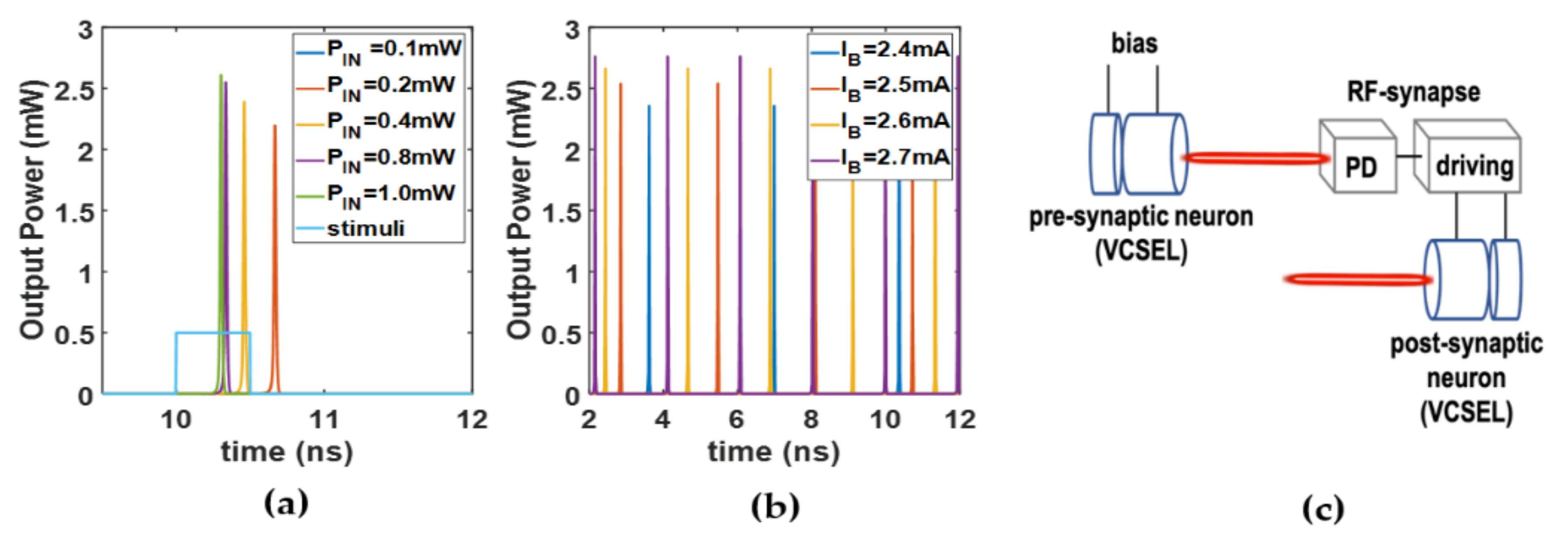
2.1. VCSEL-Neuron Modeling and Dynamic Regimes

The model used to describe the two-section VCSEL-neuron is described by the following rate equations [38]:
d n g d t = Γ g g g S k e τ p h λ h c V g P I N i = 1 N ω i τ p h λ h c V g P i o n g n 0 g n g τ g + I g e V g
d n a d t =   Γ a g a n a n 0 a S n a τ s
d S d t = Γ g g g n g n 0 g S + Γ a g a n a n 0 a S S τ p h + β B r n g 2
The subscript g and a refer to gain and absorber area, respectively. S represents the photon density in the cavity and n g / a is the electron density in the corresponding area. The term k e τ p h P I N λ h c V g in (1) simulates the electrically injected input, where k e is the coupling strength of the external signal, τ p h the photon lifetime, P I N is the power of the input electric signal, h is the Plank’s constant, c is the speed of light, λ is the VCSEL’s wavelength and V g is the cavity volume. The term i = 1 N ω i τ p h P i o λ h c V g represents the weighted sum of electrical inputs from presynaptic neurons where ω i is the weight of the i t h synapses and P i o = η c Γ g S i V g h c τ p h λ is the power originating form the i t h presynaptic neuron, where η c is the power coupling coefficient, Γ g is the confinement factor and S i is the photon density at the i t h presynaptic neuron. Other parameters used in this work are the electron’s charge e , pumpcurrent I g , the spontaneous emission coefficient β , the bimolecular recombination coefficient B r , the differential gain at every section g g / a and the transparency carrier density n 0 g / 0 a . There parameters used in this work are typical quantum-well VCSEL parameters and are provided in Table 1.
The utilized VCSELs are biased in two distinctive dynamic regimes: the excitable regime and the spiking regime. In general, VCSELs in the excitable regime produce a spike only if the injected electrical stimuli exceed a certain threshold (integrate-and-fire) [9]. For example, for an electrical input power (bias current) of PIN = 0.1 mW or lower no spike is detected (subthreshold input) while for higher PIN, the threshold condition is satisfied and the VCSEL produces a single spike (Figure 1a). Moreover, as the power level increases the latency of the spike decreases, encoding the input’s strength in the timing of the spikes (temporal encoding). On the other hand, a VCSEL in the spiking regime constantly produces spikes of period Tsp, where Tsp is the interspike interval [9]. Figure 1b demonstrates that for the investigated VCSELs, the variation of the Tsp is inversely proportional to the input power. Before presenting a layer-by-layer analysis, it is critical to highlight that the proposed neural structure relies on electro-optic synapses (Figure 1c); meaning that the optical output of each VCSEL is recorded by a photodiode (PD) with a bandwidth that is matched by spike duration. The electrical signal generated by the PDs is fed to an analogue driving circuit that weighs, sums and modifies the electrical bias of subsequent photonic neurons. This approach is considered very efficient in terms of bandwidth and flexibility, whereas it allows a straightforward implementation of neural excitation and inhibition. Moreover, it is by far more beneficial compared to power hungry digital solutions. In particular, a positive weight (excitation) corresponds to an increase in the forward bias of the VCSEL, while a negative weight (inhibition) is linked to a decrease in the bias current, driving the laser away from its threshold [9].

2.2. Building Blocks of the Network

As already mentioned, the proposed PSCNN network is a photonic adaption of [36]. It consists of five layers designated as the Contrast Detection Layer (CDL), the First Convolutional Layer (CL1), the Second Convolutional Layer (CL2), the Third Convolutional Layer (CL3) and the Output-Classification Layer as shown in Figure 2. Each of these layers consists of neurons, which in our approach are assumed to be two-section gain-absorber VCSELs. Furthermore, between two consecutive layers a synchronization layer is used. This modification is imperative for the proper function of the PSCNN due to the time-multiplexing; it ensures the simultaneous injection of spikes at every layer. To shed light on every aspect of our network an extensive description of each layer’s structure and function follows.

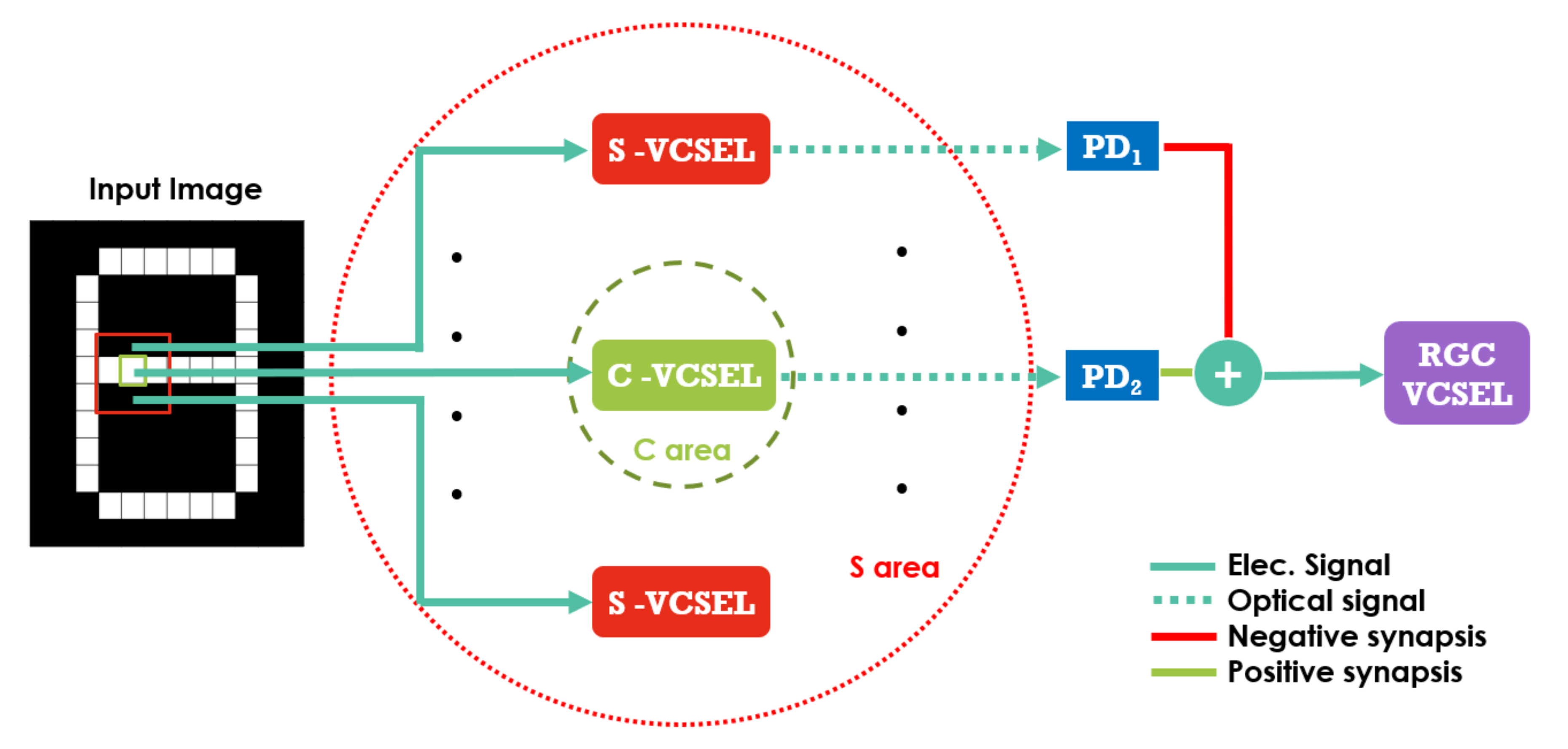
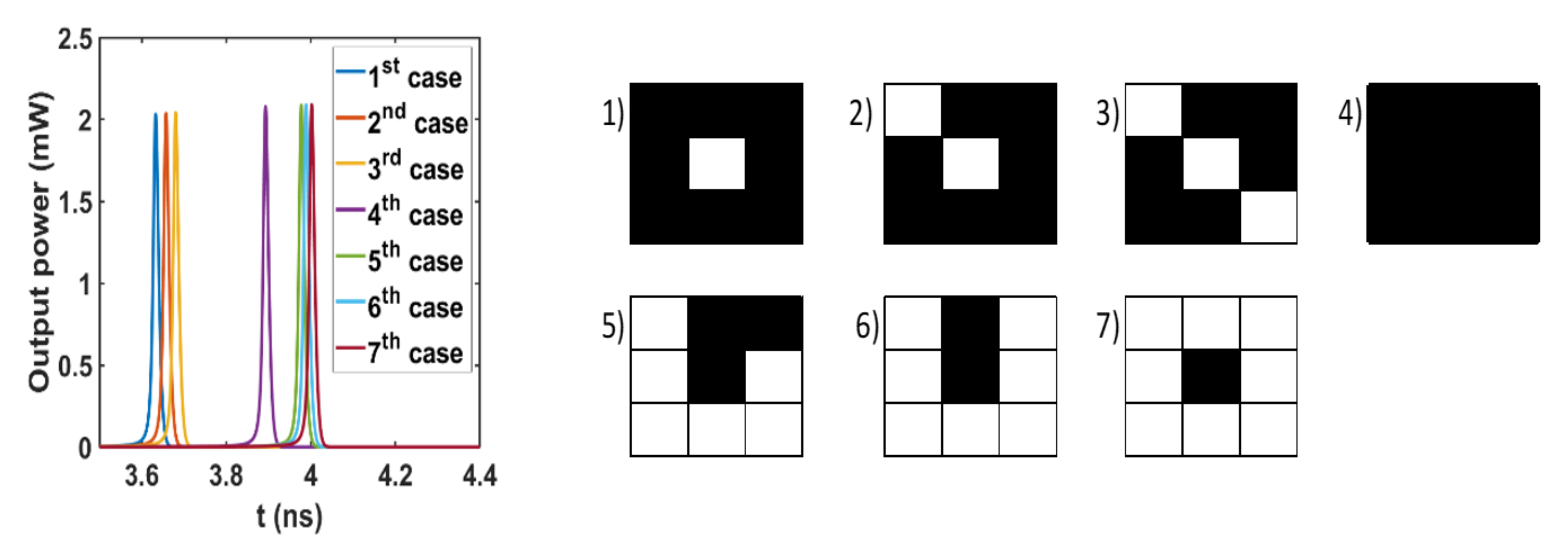
2.2.1. Contrast Detection Layer (CDL)

As stated above, the proposed network is a photonic adaptation of a SCNN [36]. In this case, the first step of processing incorporates a difference of gaussian filter (DoG) that encodes the pixel’s contrast to the spike latency. In our case, we replace this digital processing step with a bioinspired neural structure that partially mimics the operation of the retina ganglion cell (RGC) in the mammalian eye. In order to demonstrate the similarity of the digital filters with RGC, we provide an in-depth overview of its function. In biological systems, RGC’s task is to transform the analogue optical signals from the eye’s retina into a series of spikes (electric potentials) which can then be processed by the brain. The contrast of the input image is encoded to the repetition frequency of these spikes (rate encoding). More specifically, each RGC has its own receptive field which receives optical input from a specific area of the eye retina. The RGC’s receptive field is divided into two regions, namely the Center (C) and the Surround (S) (see Figure 3). The firing rate is governed by the intensity contrast of inputs in the S and C regions [39].
In our work, a set of 10 VCSELs-neurons is used so as to emulate the RGC. More specifically, the first nine neurons realize the RGC’s receptive field while the 10th neuron emulates the operation of a single RGC cell. As far as the receptive field is concerned, the 9 VCSEL-neurons are organized in a 3 × 3 layout, where each one is associated with a specific area of the receptive field. In this scheme, the C area is implemented by a single excitatory neuron (Figure 3 green C-VCSEL) located at the center of the 3 × 3 layout, whereas the S area is implemented by 8 inhibitory neurons (Figure 3 red S-VCSELs) surrounding the C-neuron. C-VCSEL and S-VCSELs are biased at the excitable regime which corresponds to an integrate-and-fire operation [9]. Their outputs are integrated by two photodiodes, PD1 for the S-neurons and PD2 for the C-neuron (Figure 3). The electrical outputs from the two PDs are weighted and summed (the negative weight for PD1 and the positive weight for PD2) before driving the RGC neuron, which is biased at the spiking regime, meaning that it fires spikes at a constant firing rate under no injection [9].
However, DοG filters dictate for a slightly different operation [36], for this reason, we modified the typical RGC so as to act as a Contrast Detection Layer (CDL). This variation of the typical RGC encodes the information-contrast of the images not at the firing rate, but on the latency of the generated spikes [40].
In detail, CDL, in our case, scans the image pixel by pixel and encodes the contrast of each pixel (injected to C-VCSEL) with respect to its surrounding ones (injected to the S-VCSELs) at the latency of the generated spike event. In order to accomplish this, a scanning window (SW) (Figure 3 red box in input image) of 3 × 3 pixels is formed with the processing pixel located at the center. When a pixel in the SW is white, then its input power is a rectangular pulse of 0.2 mW with 5 ns duration. When a pixel is black, then the input power is set to a lower power amplitude 2 μW while having the same duration as before. The 5 ns time slot will be referred as Tep and is linked to the inherent refractory period of the VCSEL-neurons used in this work. These electrical input signals associated with each SW drive the C and S neurons of the CDL, whose optical outputs are integrated, weighted and summed before they are injected in the RGC neuron. In the 5 ns time window the RGC is able to produce only a single spike in contrast to the rate encoding scheme of biological RGC. The latency of this specific spike encodes the contrast of the center pixel of the SW that is imposed on the CDL.
Τo understand the way in which CDL encodes pixel’s contrast at the timing of the spikes, the following analysis is given. When the input of a C-neuron corresponds to a white pixel whereas the S-neurons have no input (black pixels) (Figure 4 case 1) the RGC will generate a pulse at t1 (C-ON and S-OFF). In this case, the central pixel has the greatest possible contrast with respect to its surrounding pixels. However, apart from the C-neuron, if one of the S-neurons is also stimulated (Figure 4 case 2) then the pulse will be produced at a time t2 > t1. If two S-neurons are stimulated (Figure 4 case 3) then the spike will be produced at t3 > t2 > t1. The more S-neurons are stimulated, the greater the latency will be. The delay is attributed to the inhibitory effect of the S-neurons (negative weight). On the contrary if the C-neuron has no input but all of the S-neurons are stimulated (Figure 4 case 7) then the spike will be produced at a time t7 (t7 > t3 > t2 > t1) (C-OFF and S-ON). In this case, the central pixel exhibits the highest negative possible contrast with respect to its surrounding pixels. Moreover, if one of the S-VCSELs has no input, then the pulse of the RGC neuron will be produced at t6 (t7 > t6 > t3 > t2 > t1) (Figure 4 case 6). Therefore, by varying the spatial information, the latency of the produced spike event by the RGC neuron decreases or increases.
In a typical implementation each pixel will be processed by a different CDL, which will increase the number of physical neurons. Nonetheless, by exploiting the nanosecond refractory period of VCSELs, we devise a more hardware friendly approach, employing only a single CDL which serially scans every pixel of the input image. When the processing of a single pixel is completed, the SW is shifted by one pixel to the right and the same procedure is repeated for all the pixels of the image. In the case that the target pixel is located at the edge of the image, the missing SW’s pixels are assumed to be black. At this point we must stress the fact that after processing a pixel, an electrical reset signal (negative bias) should be applied to the RGC-VCSEL. Τhis reset signal forces the RGC to a subthreshold regime (resting state) so as to be able to process another pixel’s intensity originating from a different location of the image. Following this approach, the output of the CDL is a spike train. Each spike is fitted inside a specific time frame. This time-multiplexing technique is similar to [30] and enables the decrease in the number of neurons needed to process the entire image.

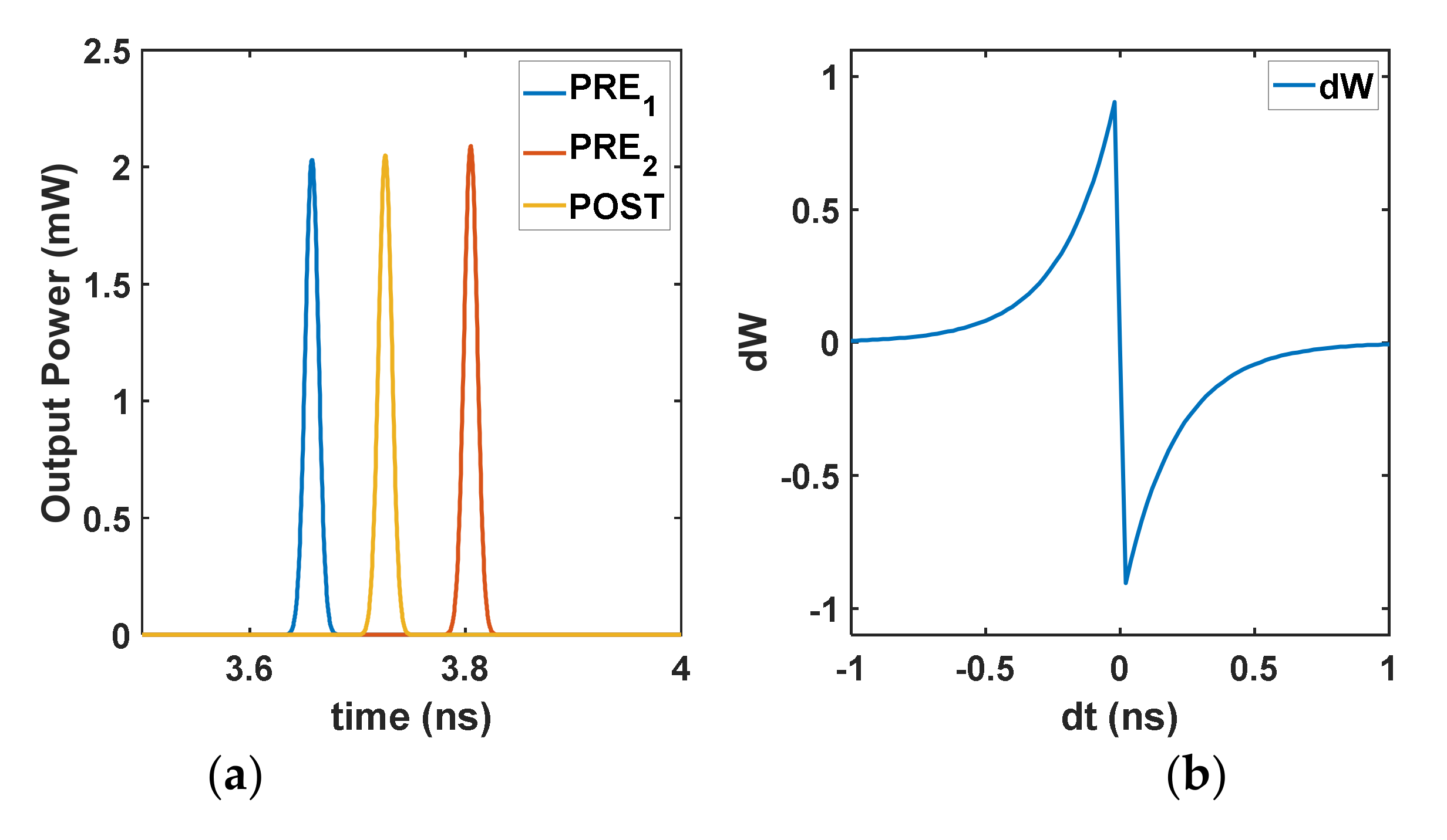
2.2.2. Synchronizing Layer

Due to the time multiplexed CDL’s output, the incorporation of a Synchronization Layer is imperative. When a Convolutional Layer processes an area of the input image, all spikes associated with this area must have a common time reference (frame) in order to properly apply the convolution function. In our case, each pixel has its contrast encoded in the timing of the generated spike events and is fitted inside a specific time slot of period Tep. So, the first spike, which encodes the contrast of the first pixel of the image, will be in the 0–Tep time slot, the second spike associated with the second pixel will be in the Tep2Tep and in general the kth spike which encodes the contrast of the kth pixel will be inside the (k − 1) TepkTep time slot. Consequently, the time reference for every spike is the beginning of each time slot (Tref = (k − 1) Tep). However, as mentioned before, spikes corresponding to different pixels should have a common time reference when they coincide at the next neural layer. Therefore, a synchronization layer is necessary: its role is to impose a (m-l) Tep delay for the kth spike, where m is the size of the convolutional window (CW) in each layer and l is the remainder of k divided by m. Using this technique, a common time reference is applied to the spikes and proper convolutional processing is enabled. The synchronization layer, in the case of electro-optic synapses (see Figure 1c) can be easily implemented through a predetermined static electrical delay line.

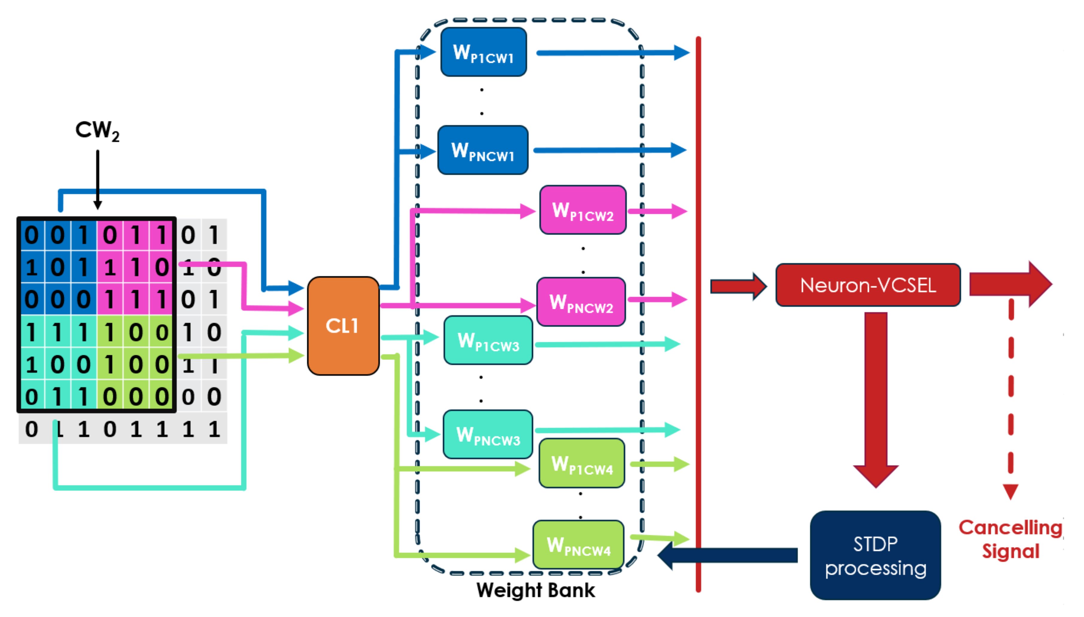
2.2.3. First Convolutional Layer (CL1)

The task of the first convolutional layer (CL1) is to learn and detect the simplest and at the same time the most frequent spike patterns associated with the images of the training set. It consists of 33 VCSELs and its processing area, designated as the Convolutional Window (CW1) consists of a 3X3 pixel layout. Each VCSEL in the CL1 layer receives 9 inputs (one for every pixel of the CW1), has a dedicated Weight Bank (WB) and it is trained so as to detect a specific pattern (Figure 5).
The training of the CL1 layer is based on STDP rule [37]. According to STDP, a neuron (post synaptic) updates its synaptic weights each time it produces a spike event. More specifically, if the neuron fires a spike event at t1, then all the synapses that provided spikes which arrived at the neuron before t1 will have their corresponding synaptic weights increased (Figure 6 PRE1). On the contrary, synapses that provided spikes that arrived after t1 will have their corresponding synaptic weights decreased (Figure 6 PRE2).
The update of the synaptic weights is summarized by the following rule
d w =   exp d t d t < 0 exp d t d t > 0
where dt = tXt1 and tX is the timing of the spike associated with the Xth synapse. After the application of the STDP rule, the new weights will be updated as
w n + 1 X = w n X + d w X a
where w(n+1)X is the updated weight of the Xth synapse, w n X is its previous weight value and a is the learning rate of the training procedure. It is worth mentioning that in our case STDP is implemented numerically, but the unsupervised nature of our scheme alongside the existence of photonic based STDP platforms [38,41], can provide hardware realizations that can offer on-chip training in near future.
After the synchronization stage, the inputs are weighted and inserted in the first neuron of the CL1. If the Input Spike Pattern (ISP) surpasses its neural threshold, then a spike will be produced. The spike event designates the recognition of the ISP by the first neuron and triggers two additional processes. The first one is the reconfiguration of its weight bank according to the STDP training algorithm. Secondly, the first neuron sends an inhibitory (cancelling) signal to all subsequent neurons in order to make them ignore this particular ISP. The cancelling signal lowers the bias of all subsequent neurons, pushing them away from the excitable regime, thus making spiking impossible for them.
On the contrary, if the ISP is not recognized by the first neuron, then it is transmitted to the second neuron after TD, which is the time needed for neuron to process the ISP, update its weights and produce the corresponding cancelling signal. The 2nd neuron then processes the ISP in a similar way as the first one. This process continues until the ISP is recognized by one of the 33 neurons of the CL1. After the ISP processing is completed, the CL1 scans the same CW1 spatial area of the next image. When all images of the training set have been scanned, the CW1 window is shifted by one pixel to the right and the whole process is repeated until all images are scanned.
Finally, when the training of the CL1 layer is completed, a weight adjustment is needed in order to make the neurons more selective to their learned pattern. The weight adjustment is crucial because a specific ISP must be recognized only by a single specific neuron of the CL1 layer. In order to explain the importance of this adjustment we must analyze the STDP algorithm. More specifically, as a neuron is trained via the STDP algorithm, its weights increase and decrease continuously. If this process continues indefinitely, then the STDP will eventually lock to the spike associated with the smallest latency and ignore all the others [38]. In order to avoid this issue and to force our system to take into account more than a single spike, the maximum and minimum weight values are set to WMAX and WMIN. In our simulation we set WMAX = 0.45 and WMIN = −1. Suppose for example that the WB of the first neuron after training acquires the following values w1 = [−1 −1 0.45 −1 −1 0.45 −1 −1 0.45].
In this case, if the input is ISP1 = 0 0 1 0 0 1 0 0 1 (0 for black pixel 1 for a white pixel) then the neuron will be activated. However, if the input is ISP2 = 0 0 1 0 0 0 0 0 1 then there is a risk that the neuron will be activated again if WMAX is too high. For this reason, the final weights of each WB must be adjusted in such a way that only a single neuron will be able to respond to ISP1. In order to achieve the aforementioned spiking behavior, positive values of w1 must be decreased down to a certain level, which will permit the activation of the neuron by exactly three spikes. This weight adjustment depends on the number of weights which have a value between 0.9WMAX and WMAX and not on their exact spatial distribution. Depending on that number, the final weights are set as shown in Table 2 below.
After the weight adjustment of the WBs of the CL1 layer is accomplished, the computed weight values will apply to the hardware synapses and the training of the CL1 is complete. After the training phase, TD delays can be ignored, since the neurons in the CL1 layer at this point have successfully learned the input patterns. During the inference mode, the incoming SP is simultaneously inserted into all neurons of CL1. The maximum number of neurons that will fire a spike at every ISP is one and is the neuron that has successfully learned the incoming pattern.

2.2.4. Second Convolutional Layer (CL2)

The CL2 has 16 VCSELs and it receives inputs from 4 CW1s in a 2 × 2 layout. In this way, its processing area (CW2) is equivalent to a square area of 6 × 6 pixels in the original image. The CW2 window is similar to the CW1, but it has two major differences: a different total number of inputs and a modified training algorithm. With respect to the number of inputs, since the CW2 window receives 4 CW1 windows and since the CW1 windows will represent one of 33 learned patterns from CL1 each time, the total number of inputs at the CW2 window is equal to 4 × 33 = 132. Its first 33 inputs correspond to the first CW1, the next 33 inputs (Input No 34—No 66) correspond to the second CW1 and so on (Figure 7).
With respect to the training algorithm, in CL1 every neuron receives nine inputs—one for every pixel of the image. After the generation of a spike event, the STDP rule updates the weight values of the associated WB. However, in the case of CL2, each neuron receives only 4 synaptic inputs—one for every pattern in each separate CW1. When a neuron at the CL2 fires a spike, the weight of the synapse associated with the excitation of the neuron will be increased. However, the neuron will receive no input from the remaining synapses, which means that if the STDP rule is applied in this case, their corresponding weight values will stay unmodified. Thus, the decrease in the synaptic weights with this scheme is not possible. For this reason, at the CL2 layer a different training algorithm is used, according to which the weight of the synapse associated with the excitation of a neuron is increased by a constant value, while all others are decreased by the same value. The new training algorithm is given by the following rule
d W = 0.1 a b s e n c e   o f   s p i k e 0.1 p r e s e n c e   o f   s p i k e
After the training of the CL2 layer is completed, the weights have to be adjusted in a manner similar to the case of the CL1 layer. The TD delays corresponding to the previous synchronization layer that were required for the training procedure can again be safely ignored afterwards.

2.2.5. Third Convolutional Layer (CL3)

The CL3 has 8 neurons and its Convolutional Window (CW3) receives input from 2 CW2 windows in a 1 × 2 layout, thus forming a window which corresponds to an area of 6 × 12 pixels of the original image. The total number of inputs from the CL2 layer will be 2 × 16 = 32, since CL2 consists of 16 neurons. The training rule used in this layer is identical to the one used in the CL2 layer. After the training of the CL3 is completed, the respective TD delays can be safely ignored and the training of the final Classification Layer can begin.

2.2.6. Classification Layer

The classification layer comprises 4 neurons, as the number of input images that are going to be classified by the PSCNN. Each neuron of this layer receives 2 × 8 = 16 inputs and its neural activity designates the classification of the input image to a specific class, meaning that the input image is successfully recognized. Its structure and training procedure is identical to the CL2 and CL3. When the final output layer is trained TD delays will be ignored and the inference and validation of the PSCNN can begin.

3. Results

In this section, the numerical results with regards to the training and inference operation of the proposed PSCNN will be presented. At first, details about training and inference operation are shown. After that, we clarify the limits of our network by performing a noise analysis on the PSCNN. Furthermore, we discuss the bandwidth limitations introduced by the photodiodes and the tuning capability of the PSCNN to reduce the number of neurons at the cost of processing time. Lastly, a comparison between the PSCNN and other equivalent networks is presented.

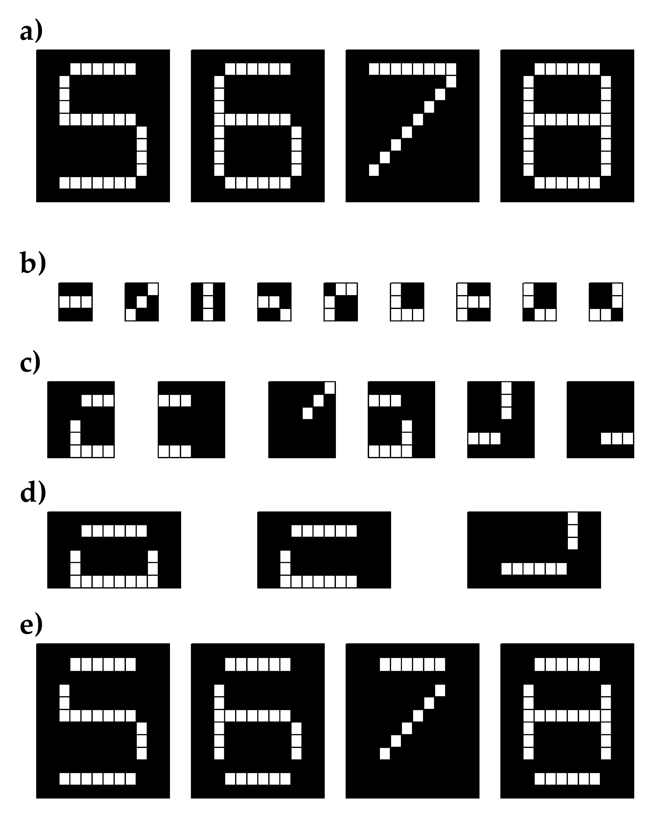
3.1. Training and Interference
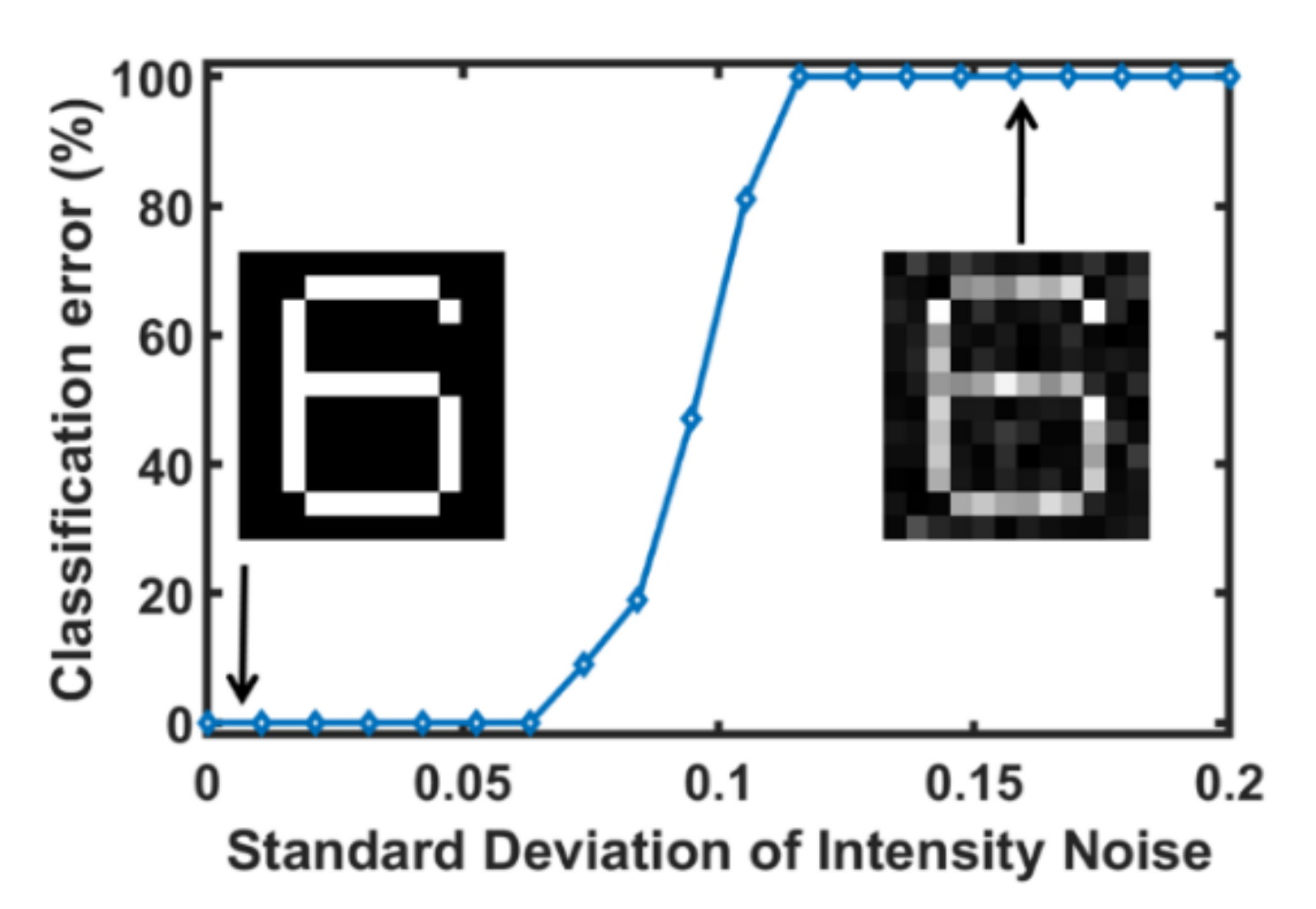
As a validation scenario, we trained the network with a set of 100 images depicting four 12 × 12 pixel, black and white decimal digits ranging from 5 to 8 (Figure 8a). The images were inserted to the network sequentially and the pixel values were mapped to the bias of the VCSELs at the CDL. It is of utmost importance to point out that no data-labeling was performed, and weight adaptation occurred through an unsupervised version of STDP. The first convolutional layer aimed for 33 target patterns. Typical examples are shown in Figure 8b. In the CL2 the network was trained to detect combinations of patterns from the CL1 layer (Figure 8c). The shift of the CW2 was equal to the number of pixels per row (6 pixels horizontally). After the horizontal scanning of the image was completed, the CW2 was shifted 6 pixels downwards and the same procedure was repeated until all of the training images were scanned. The detailed scanning process of the CL1 alleviates the need for more complex training in the CL2 and CL3 and no spatial overlap is needed in them. The reason is that the CL1 identified most of the basic patterns of the images. Based on this, CL2 patterns are a combination of simpler patterns which are identified in an unsupervised manner in the CL1 (Figure 8c). The same applies to the CL3 Figure 8d. Following these basic training rules and without labeling the data, the Classification Layer of the network self-constructed an abstract version of the original images and classified the input images based on their similarity with the abstracted versions (Figure 8e). In order to validate our method, we repeated the training process but in this case we changed the training set by using images illustrating the digits 1–4. The network adapted to new features and patterns, recalibrating the weights. Furthermore, it is worth mentioning that we have not used a data set comprising of all the digits (0–9) due to the fact that training even for such a small dataset was time-consuming. This stems from the fact that we realized a full-scale simulation, incorporating multiple layers and dozens of physically accurate VCSELs, instead of simplistic spiking models. Towards this direction, we adapted our PSCNN model to be compatible with parallel processing through 4352 GPU cores (Nvidia RTX 2080Ti) so as to speed-up computation [42]. Although, in principle, the whole network could be computed in parallel, we managed to evaluate only the first two layers (CDL and CL1). This stemmed from the need to keep long time-traces (temporal information) among layers that in turn lead to an extensive memory demand that could not be handled by our GPU system. Fortunately, CDL and CL1 have the vast majority of network’s neurons; thus, even with these restrictions, the overall speed enhancement achieved was ×30. This enhancement resulted in a training time of 25 min/image, which is acceptable considering the number and complexity of the simulated model. On the other hand, this execution speed increase, resulted in negligible inference time, even when using the whole dataset.

3.2. Noise Analysis

In order to explore the performance of the trained PSCNN, we assumed typical thermal and shot noise at the photodiodes of the electro-optic synapses, as the dominant perturbing mechanism. We varied the level of noise and evaluated the impact to the classification error when the network was inferring a set of 100 images which consists of all the four digits (‘5′, ‘6′, ‘7′ and ‘8′). Simulations provided evidence that even for low Signal-to-Noise Ratio (SNR < 10 dB) and for the above-described simple classification task, there was no impact in classification error. This resiliency can be attributed to the integrate-and-fire nature of the VCSEL-neurons and the relative, large integration time. In particular, even though the instant input power of the pixel may exhibit significant variation, the average input power remains approximately the same. Consequently, the timing of the produced spikes from CDL’s receptive field neurons is not severely affected.
Since, the PD Gaussian noise did not affect the performance of our network, we took into consideration a different noise source that corresponds to mean intensity variation at each pixel. In this scenario, the intensity of each pixel is perturbed compared to the nominal value resulting in a distorted version of the original image (Figure 9). This type of perturbation affects the contrast in each SW and thus alters the timing of spikes. So as to model such an effect we added to the mean intensity of each pixel a random variation, drawn from a normal distribution with different standard deviations (see inset of Figure 9). These intensity variations are mapped to the input power of the neurons at the CDL. The PSCNN is considered trained and in this case is set to an inference mode.
The set of 100 images, which comprised all of equivalently distributed digits ‘5′ to ‘8′, was fed to the network and the classification error was computed in a set containing all possible digits. In Figure 9 the total classification error is presented (for all digits) versus the standard deviation of pixel noise. It can be seen that the classification error of our system remained low for perturbations with standard deviation up to 6% of the nominal value, while an abrupt increase can be observed for higher values.

3.3. Bandwidth Limitations

To evaluate bandwidth’s impact on the proposed PSCNN, an analysis of the two modes of operation, training and inference, is presented. When the network operates in inference or training mode then there are bandwidth limitations related to the electro-optic synapses; meaning that optical spikes generated by the neurons are detected by analog PDs (with appropriate bandwidth). The electrical spikes generated are processed also in the analog domain and are used to modulate (excite) subsequent neurons; meaning that the spiking nature of the pulses can be reproduced with reliability by PDs and electronics of 20 GHz that can drive state of the art VCSELs of similar modulation bandwidth. Furthermore, aiming to render our scheme hardware-friendly and avoid high performance PDs, we can use photodiodes with lower bandwidth at the cost of lower spike amplitude. This drawback can be amended by scaling the synaptic weights, which will be realized using RF electronics [9]. More importantly, real-life VCSELs generate neural spikes with significantly broader temporal width (>200 ps) [43], compared to the VCSEL assumed in this work. In this case, the minimum bandwidth requirements drop significantly (1–5 GHz) and can be realized with low-cost PDs. This spike duration increase could also affect the refractory period of the VCSELs; thus, it could potentially affect time-multiplexing capabilities but not accuracy. Taking into consideration that nanosecond refractory period is extreme for realistic image processing, but the basic concept of this work remains valid even with such a modification. In terms of training, bandwidth demands are anticipated to be enhanced, mainly due to the STDP technique. In particular, hardware realizations of STDP dictate the precise knowledge of the time of arrival of each spike at each synapse, so as to preserve accuracy [38,41]. Taking into consideration that potentiation/depression window in our case is ≈1 ns and the refractory period is 5 ns, then a 20 GHz bandwidth can guarantee temporal accuracy. An alternative approach could include offline training through a physically accurate model and limiting the hardware module in an inference mode. In this case, structural deviations could be fine-tuned through optimization of spike delays at the synchronization layer and by adjusting the synaptic weights.

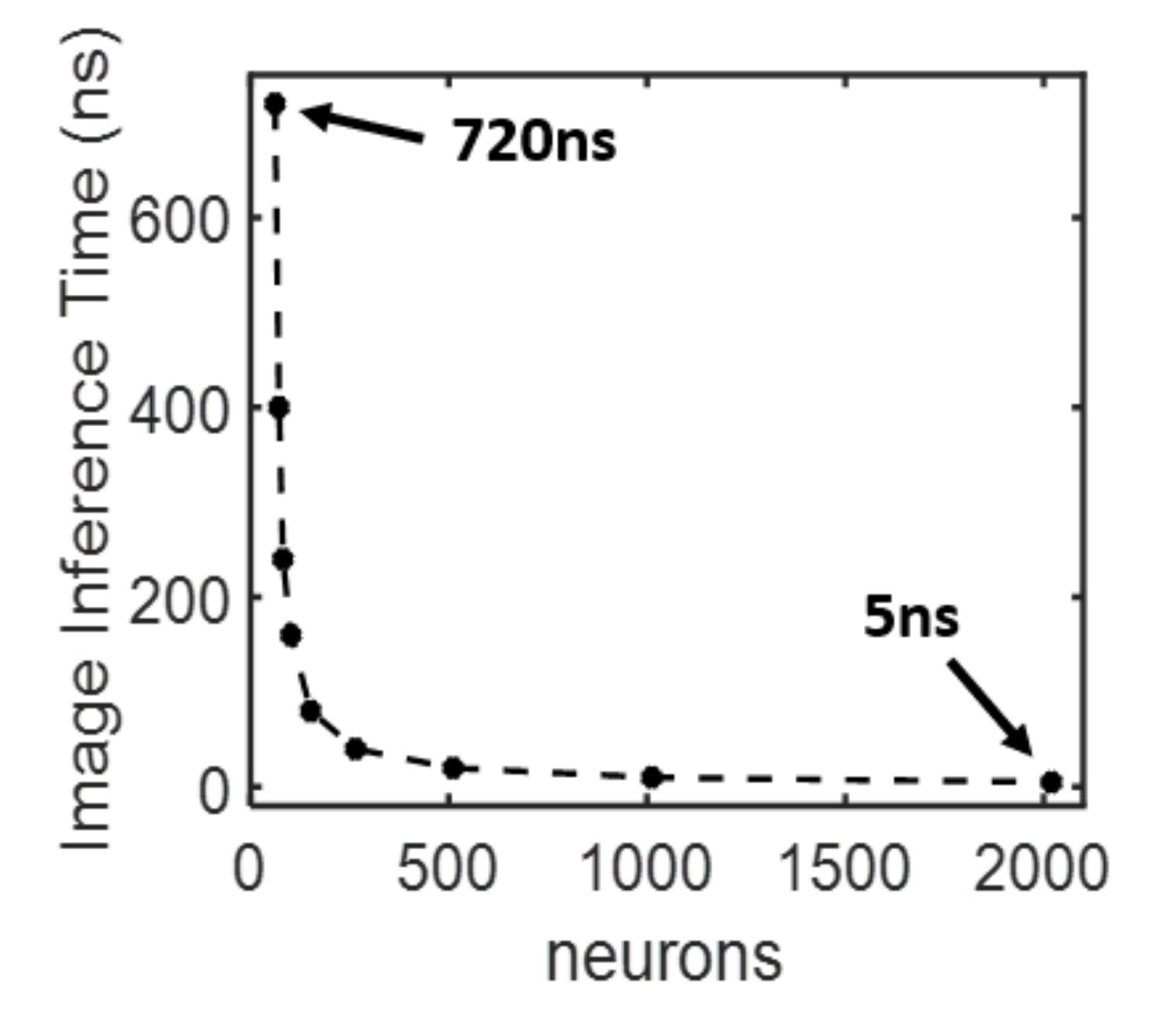
3.4. Processing Time versus Neuron Count

One of the key aspects of our network is its ability to adjust the processing time by varying the number of pixels that are time-multiplexed and thus are processed by the same physical neuron. In Figure 10 this trade-off is illustrated by plotting the inference time for one typical image (12 × 12 pixel) versus the number of physical neurons in the network. The minimum number of neurons, for the five-layer network (maximum multiplexing) is 62, resulting in a processing time of 720 ns/image (12 × 12 × 5 ns). Moving to the other end, thus employing the maximum number of neurons (2020) leads to an inference time governed by the refractory period (5 ns). In this case, each pixel is processed by a specific CDL, while every Convolutional Window is processed by its own Convolutional Layer. Obviously, this trade-off can lead to larger networks with Mframe/s capability suitable for demanding imaging applications such as aerospace, or to hardware-friendly realizations suitable for pragmatic applications (<200 frame/s). For example, in this work, the fully multiplexed 62 neuron scheme can allow the processing of 144 pixels in 720 ns leading to a processing rate of 1.38 M frame/s.

3.5. Comparative Study with Previous VCSEL-Based Neural Networks

In [30], the experimental data from a VCSEL based neuron are presented. This implementation detects specific patterns at GHz rates. Moreover, the input images are processed via a time multiplexing technique, which uses the same neuron to process different areas of the image, reducing in this way the number of actual neurons. On the other hand, in this scheme synaptic weights are fixed in advance and no training takes place. In [29] numerical results from a two-layer VCSEL-based spiking network which classifies numerical digits (0–9) are presented. In particular, [29] uses a timing-encoding scheme for data encoding while training is accomplished under a supervised STDP algorithm. Except for the training algorithm, the two networks have some key differences. First of all, Ref [29] deploys Convolutional Layers as a preprocessing step in order to moderate noise impact. In our work, Convolutional Layers are used to extract features from the input images, which offers our network the potential to be used in the classification of more complex images. Second, every pixel of the input image is processed by a different neuron. Since the input images have 400 pixels, a total of 410 neurons (400 neurons for pixel processing and 10 neurons for classification) is required to properly classify the images of the ten digits. In our network, thanks to time multiplexing only 62 are needed in order to classify 4 digits (‘5’, ‘6’, ‘7’ and ‘8’). Moreover, for the classification of all ten digits a total number of 87 neurons will be needed: specifically, 10 neurons for the Contrast Detection Layer, 32 at the first convolutional layer, 21 at the second, 14 neurons at the third and 10 neurons at the output layer. Moreover, Ref [29] deploys a two-layer network while in our case a ‘deep’ five-layer convolutional neural network is implemented for the first time to our knowledge. Furthermore, the processing time of the images is fixed to 30 ns per image. In our case, the insertion of multiple layers permits the tuning of the processing times ranging from 5 ns (full parallel processing) to 720 ns (minimum number of neurons used). Lastly, in [29] the classification error is linearly dependent on the network’s noise. On the other hand, our network has a sigmoid dependance from the noise (Figure 9). This makes our network better for low intensity conditions while [29] is better suited for noisy environments.

4. Conclusions

At a glance, the proposed neural scheme is an optical adaptation of a SCNN [36], aiming to inherent the performance of its software counterpart and at the same time provide radical new advantages by replacing software functions and nodes with photonic neurons. The resulting PSCNN comprises VCSEL neurons which are arranged in multiple “deep” neural layers. Each layer provides a different operation, ranging from pixel-contrast encoding to spike-latency, spike time-multiplexing and SCNNs for pattern recognition. In our work, the training of the neuromorphic scheme relies on an unsupervised version of STDP, whereas each node’s response was computed through a physically accurate numerical model. Furthermore, in order to address the high neuron count dictated by SCNNs we realized a time-multiplexing strategy, where different pixels of the image are processed by the same physical laser-neurons. This technique allowed the replication of a software based SCNN with 2020 neurons with only 62 laser-nodes and an inference rate of 1.38 M frame/s for 144 pixel images. Furthermore, we generated an artificial set of images depicting numerical digits so as to train/test the classification capabilities of the proposed network. The results confirm that the integrate-and-fire nature of the VCSEL neurons renders our scheme extremely resilient to typical white noise sources (shot, thermal noise), while variations at the mean intensity of pixels affect image contrast and thus impact spike timing, leading to high classification error.

Author Contributions

M.S. developed the numerical model and the neural network, did the majority of the simulations and wrote the manuscript with help from all co-authors. S.D. was responsible for GPU simulations. G.S. and A.B. provided discussion/input on numerical modelling and neural structure simulation. C.M. was the initiator of this project and was supervising the work. All authors have read and agreed to the published version of the manuscript.

Funding

This research was funded by the EU H2020 NEOTERIC project (871330) and the Hellenic Foundation for Research and Innovation (HFRI) and the General Secretariat for Research and Technology (GSRT), under grant agreement No 2247 (NEBULA project).

Institutional Review Board Statement

Not applicable.

Informed Consent Statement

Not applicable.

Data Availability Statement

Not applicable.

Acknowledgments

This project has received funding from the EU H2020 NEOTERIC project (871330) and the Hellenic Foundation for Research and Innovation (HFRI) and the General Secretariat for Research and Technology (GSRT), under grant agreement No 2247 (NEBULA project).

Conflicts of Interest

The authors declare no conflict of interest.

References

  1. Abu-Mostafa, Y.S.; Psaltis, D. Optical neural computers. Sci. Am. 1987, 256, 88–95. [Google Scholar] [CrossRef] [Green Version]
  2. Mahapatra, N.R.; Venkatrao, B. The processor-memory bottleneck: Problems and solutions. Crossroads 2008, 5, 2. [Google Scholar] [CrossRef]
  3. Miller, D.A.B. Device Requirements for Optical Interconnects to Silicon Chips. Proc. IEEE 2009, 97, 1166–1185. [Google Scholar] [CrossRef] [Green Version]
  4. Indiveri, G.; Liu, S.-C. Memory and information processing in neuromorphic systems. Proc. IEEE 2015, 103, 1379–1397. [Google Scholar] [CrossRef] [Green Version]
  5. Roy, K.; Jaiswal, K.; Panda, P. Towards spike-based machine intelligence with neuromorphic computing. Nature 2019, 575, 607–617. [Google Scholar] [CrossRef]
  6. Mainen, Z.; Sejnowski, T. Reliability of spike timing in neocortical neurons. Science 1995, 268, 1503–1506. [Google Scholar] [CrossRef] [Green Version]
  7. Hopfield, J.J. Pattern recognition computation using action potential timing for stimulus representation. Nature 1995, 376, 33–36. [Google Scholar] [CrossRef]
  8. Gautrais, J.; Thorpe, S. Rate coding versus temporal order coding: A theoretical approach. Biosystems 1998, 48, 57–65. [Google Scholar] [CrossRef]
  9. Prucnal, P.R.; Shastri, B.J.; Ferreira, T.; Nahmias, M.A.; Tait, A.N. Recent progress in semiconductor excitable lasers for photonic spike processing. Adv. Opt. Photonics 2016, 8, 228–299. [Google Scholar] [CrossRef]
  10. Burd, T.D.; Brodersen, R.W. Energy efficient CMOS microprocessor design. In Proceedings of the 28th Annual Hawaii International Conference on System Sciences, Wailea, HI, USA, 3–6 January 1995. [Google Scholar]
  11. Prucnal, P.R.; Shastri, B.J. Neuromorphic Photonics; CRC Press: Boca Raton, FL, USA, 2017. [Google Scholar]
  12. Caulfield, H.J.; Dolev, S. Why future supercomputing requires optics. Nat. Photonics 2010, 4, 261–263. [Google Scholar] [CrossRef]
  13. Shastri, B.J.; Nahmias, M.A.; Tait, A.N.; Rodriguez, A.W.; Wu, B.; Prucnal, P.R. Spike processing with a graphene excitable laser. Sci. Rep. 2016, 6, 19126–19138. [Google Scholar] [CrossRef] [PubMed] [Green Version]
  14. Coomans, W.; Gelens, L.; Beri, S.; Danckaert, J.; Sande, G.V. Solitary and coupled semiconductor ring lasers as optical spiking neurons. Phys. Rev. 2011, 84, 36209. [Google Scholar] [CrossRef] [PubMed] [Green Version]
  15. Van Vaerenbergh, T.; Fiers, M.; Mechet, P.; Spuesens, T.; Kumar, R.; Morthier, G.; Schrauwen, B.; Dambre, J.; Bienstman, P. Cascadable excitability in microrings. Opt. Express 2012, 20, 20292–20308. [Google Scholar] [CrossRef] [PubMed] [Green Version]
  16. Koen, A.; van Vaerenbergh, T.; Fiers, M.; Mechet, P.; Dambre, J.; Bienstman, P. Excitability in optically injected microdisk lasers with phase controlled excitatory and inhibitory response. Opt. Express 2013, 21, 26182–26191. [Google Scholar] [CrossRef] [Green Version]
  17. Sarantoglou, G.; Skontranis, M.; Mesaritakis, C. All Optical Integrate and Fire Neuromorphic Node Based on Single Section Quantum Dot Laser. IEEE J. Sel. Top. Quantum Electron. 2019, 26, 1900310. [Google Scholar] [CrossRef]
  18. Goulding, D.; Hegarty, S.P.; Rasskazov, O.; Melnik, S. Excitability in a quantum dot semiconductor laser with optical injection. Phys. Rev. 2007, 98, 4–7. [Google Scholar] [CrossRef] [PubMed] [Green Version]
  19. Yacomotti, A.M.; Monnier, P.; Raineri, F.; Bakir, B.B.; Seassal, C.; Raj, R.; Levenson, J.A. Fast thermo-optical excitability in a two-dimensional photonic crystal. Phys. Rev. 2006, 97, 143904. [Google Scholar] [CrossRef]
  20. Brunstein, M.; Yacomotti, A.M.; Sagnes, I.; Raineri, F.; Bigot, L.; Levenson, A. Excitability and self-pulsing in a photonic crystal nanocavity. Phys. Rev. 2012, 85, 31803. [Google Scholar] [CrossRef]
  21. Garbin, B.; Goulding, D.; Hegarty, S.P.; Huyet, G.; Kelleher, B.; Barland, S. Incoherent optical triggering of excitable pulses in an injection-locked semiconductor laser. Opt. Lett. 2014, 39, 1254–1257. [Google Scholar] [CrossRef]
  22. Garbin, B.; Javaloyes, J.; Tissoni, G.; Barland, S. Topological solitons as addressable phase bits in a driven laser. Nat. Commun. 2015, 6, 5915. [Google Scholar] [CrossRef] [Green Version]
  23. Aragoneses, A.; Perrone, S.; Sorrentino, T.; Torrent, M.C.; Masoller, C. Unveiling the complex organization of recurrent patterns in spiking dynamical systems. Sci. Rep. 2014, 4, 4696–4712. [Google Scholar] [CrossRef] [PubMed] [Green Version]
  24. Giudici, M.; Green, C.; Giacomelli, G.; Nespolo, U.; Tredicce, J.R. Andronov bifurcation and excitability in semiconductor lasers with optical feedback. Phys. Rev. 1997, 55, 6414–6418. [Google Scholar] [CrossRef]
  25. Hurtado, A.; Javaloyes, J. Controllable spiking patterns in long-wavelength vertical cavity surface emitting lasers for neuromorphic photonics systems. Appl. Phys. 2015, 107, 241103. [Google Scholar] [CrossRef] [Green Version]
  26. Hurtado, A.; Schires, K.; Henning, I.D.; Adams, M.J. Investigation of vertical cavity surface emitting laser dynamics for neuromorphic photonic systems. Appl. Phys. Lett. 2012, 100, 103703. [Google Scholar] [CrossRef] [Green Version]
  27. Nahmias, M.A.; Shastri, B.J.; Tait, A.N.; Prucnal, P.R. A leaky integrate-and-fire laser neuron for ultrafast cognitive computing. IEEE J. Sel. Top.Quantum Electron. 2013, 19, 1800212. [Google Scholar] [CrossRef]
  28. Hurtado, A.; Henning, I.D.; Adams, M.J. Optical neuron using polarization switching in a 1550 nm-VCSEL. Opt. Express 2010, 18, 25170–25176. [Google Scholar] [CrossRef] [PubMed] [Green Version]
  29. Robertson, J.; Wade, E.; Kopp, Y.; Bueno, J.; Hurtado, A. Towards Neuromorphic Photonic Networks of Ultrafast Spiking Laser Neurons. IEEE J. Sel. Top. Quantum Electron. 2019, 26, 1. [Google Scholar] [CrossRef] [Green Version]
  30. Robertson, J.; Zhang, Y.; Hejda, M.; Adair, A.; Bueno, J.; Xiang, S.; Hurtado, A. Convolutional Image Edge Detection Using Ultrafast Photonic Spiking VCSEL-Neurons. arXiv 2020, arXiv:2007.10309. [Google Scholar]
  31. Xiang, S.; Ren, Z.; Zhang, Y.; Song, Z.; Guo, X.; Han, G.; Hao, Y. Training a Multi-Layer Photonic Spiking Neural Network with Modified Supervised Learning Algorithm Based on Photonic STDP. IEEE J. Sel. Top. Quantum Electron. 2021, 27, 7500109. [Google Scholar] [CrossRef]
  32. Xiang, S.; Ren, Z.; Song, Z.; Zhang, Y.; Guo, X.; Han, G.; Hao, Y. Computing Primitive of Fully VCSEL-Based All-Optical Spiking Neural Network for Supervised Learning and Pattern Classification. IEEE J. Sel. Top. Quantum Electron. 2020, 1–12. [Google Scholar] [CrossRef]
  33. Robertson, J.; Hejda, M.; Bueno, J.; Hurtado, A. Ultrafast optical integration and pattern classification for neuromorphic photonics based on spiking VCSEL neurons. Sci. Rep. 2020, 10, 6098. [Google Scholar] [CrossRef] [PubMed] [Green Version]
  34. Feldmann, J.; Youngblood, N.; Wright, C.D.; Bhaskaran, H.; Pernice, W.H.P. All-optical spiking neurosynaptic networks with self-learning capabilities. Nature 2019, 569, 208–214. [Google Scholar] [CrossRef] [PubMed] [Green Version]
  35. Albawi, S.; Mohammed, T.A.; Al-Zawi, S. Understanding of a convolutional neural network. In Proceedings of the 2017 International Conference on Engineering and Technology (ICET), Antalya, Turkey, 21–23 August 2017; pp. 1–6. [Google Scholar]
  36. Kheradpisheh, S.R.; Ganjtabesh, M.; Thorpe, S.J.; Masquelier, T. STDP-based spiking deep convolutional neural networks for object recognition. Neural Netw. 2018, 99, 56–67. [Google Scholar] [CrossRef] [PubMed] [Green Version]
  37. Masquelier, T.; Guyonneau, R.; Thorpe, S.J. Competitive STDP based spike pattern learning. Neural Comput. 2009, 21, 1259–1276. [Google Scholar] [CrossRef] [PubMed]
  38. Xiang, S.; Zhang, Y.; Gong, J.; Guo, X.; Lin, L.; Hao, Y. STDP-Based Unsupervised Spike Pattern Learning in a Photonic Spiking Neural Network with VCSELs and VCSOAs. IEEE J. Sel. Top. Quantum Electron. 2019, 25, 1700109. [Google Scholar] [CrossRef]
  39. Liquon, L. Principles of Neurobiology, 2nd ed.; Taylor & Francis Group, LLC: New York, NY, USA, 2016; pp. 121–164. [Google Scholar]
  40. Thorpe, S.J.; Delorme, A.; Van Rullen, R. Spike-based strategies for rapid processing. Neural Netw. 2001, 14, 715–726. [Google Scholar] [CrossRef]
  41. Mesaritakis, C.; Skontranis, M.; Sarantoglou, G.; Bogris, A. Micro-Ring-Resonator Based Passive Photonic Spike-Time-Dependent-Plasticity Scheme for Unsupervised Learning in Optical Neural Networks. In Proceedings of the 2020 Optical Fiber Communications Conference and Exhibition (OFC), San Diego, CA, USA, 8–12 March 2020; pp. 1–3. [Google Scholar]
  42. Nvidia. Available online: www.nvidia.com/en-eu/geforce/graphics-cards/rtx-2080-ti/ (accessed on 18 December 2020).
  43. Barbay, S.; Kuszelewicz, R.; Yacomotti, A.M. Excitability in a semiconductor laser with saturable absorber. Opt. Lett. 2011, 36, 4476–4478. [Google Scholar] [CrossRef]
Figure 1. (a) VCSEL operation in excitable regime for different levels of input power. For PIN = 0.1 mW no spike is generated (under threshold stimuli) while for higher PIN values a spike is fired. Higher PIN decreases the latency and enables the timing encoding of the input’s power level. The bias current is Ib = 2.32 mA while the duration of the applied stimuli is TON = 0.5 ns. (b) VCSEL operation in spiking regime for different biases. Higher Ib decreases the Tsp (interspike interval). (c) Photonic VCSEL neurons and Radio Frequency (RF) synapse configuration, PD stands for photodiode.
Applsci 11 01383 g001
Figure 2. Photonic Spiking Convolutional Neural Network (PSCNN) architectural view. External electrical pulses according to the pixel’s intensity are inserted at the Contrast Detection Layer (CDL). White pixels are encoded as rectangular pulses with power of 0.2 mW whereas black pixels are encoded as rectangular pulses with power equal to 2 μW. CDL’s output consists of spike trains with latency proportional to each pixel’s intensity. Different pixels are processed by the same neuron in a sequential function and output spikes are multiplexed in time. When CDL’s processing is complete then the output electrical spikes are inserted in the Synchronization Layer (Synch) in order to synchronize the spikes from different pixels and fit them to a specific time frame. After the synchronization is completed, spikes are inserted into the First Convolutional Layer (CL1) which detects spike patterns (features) according to their timing. When a pattern is detected the corresponding neuron of CL1 fires a spike (feature extraction). These new spikes originating from CL1 are transmitted to the Second Convolutional Layer (CL2) in order to detect more complex patterns. The same procedure is repeated in the Third Convolutional Layer (CL3). At the Classification Layer the network is able to classify the incoming image based on the detected patterns from all CL3. Throughout the network, synchronizing procedures are necessary in order for the spikes to coincide at the next layer.
Applsci 11 01383 g002
Figure 3. VCSEL based retina ganglion cell (RGC) calculating the contrast of a specific pixel (green box). Each VCSEL takes input from a specific pixel of the SW (red box). Depending on that input, the first 9 VCSEL-neurons, which realize the receptive field of the human eye, produce spikes or remain stable. The outputs of C and S VCSELs are integrated by two photodiodes (PD) whose outputs are weighted and summed before they are injected into the RGC VCSEL. The C-VCSEL (green) has an excitatory effect (positive weight) on the RGC-VCSEL while the outputs of the S-VCSELs (red) have an inhibitory effect (negative weight). The RGC-VCSEL produces a spike for each pixel and according to the spatial distribution of the black and white pixels the spike latency is increased or decreased.
Applsci 11 01383 g003
Figure 4. Output power of the CDL for different input cases. Black boxes represent black pixels of the scanning window (SW) (no light input) while white boxes represent white pixels of the image (presence of light). While C-neurons receive input the latency is decreased. However, the activation of S-neurons augments the latency. On the contrary, when all S-neurons receive light but C-neurons do not, the latency is increased, while the activation of fewer S-neurons accelerates the produced spike.
Applsci 11 01383 g004
Figure 5. Block diagram of the first convolutional layer network during training. A specific area of the image is scanned by the contrast detection layer in order to detect pixels with high contrast (1 for black pixels and 0 for white pixels). After that the generated spikes are synchronized and entered into the neuron-VCSELs. Each neuron has its weight stored in a weight bank. When a neuron detects a pattern (fires a spike) it sends a cancelling signal to all of the following neurons (dashed lines).
Applsci 11 01383 g005
Figure 6. (a) Timing of spikes originating from the neuron under training (POST) and two other presynaptic neurons (blue and red). (b) The spike dependent plasticity (STDP) weight modification curve. According to STDP, training w1 will be increased while w2 will be decreased.
Applsci 11 01383 g006
Figure 7. CL2’s neurons layout. WPXCWZ represents weight for the input of the CL1’s neuron, which detects Pattern X in the area of CWY.
Applsci 11 01383 g007
Figure 8. (a) Four numbers used as inputs for the training of the network. Learned patterns of (b) CL1, (c) CL2 and (d) CL3. (e) The abstract version of the digits that the network identifies.
Applsci 11 01383 g008
Figure 9. PSCNN classification error for different values of the intensity noise. The intensity noise is drawn from a normal distribution whose standard deviation is expressed as a percentage of the nominal input power PIN = 0.2 mW (x-axis). For intensity noise values up to 6% (12 μW) no classification error is monitored. However, for higher values of intensity noise there is a sharp increase in network’s classification error and for a standard deviation of 11% (22 μW) the system collapses since it cannot classify the input images. In this figure, digit ‘6′ is presented as an indicative example of the intensity noise’s impact. The left image of digit ‘6′ represents the case of no intensity noise while the right one corresponds to an intensity noise of 16%.
Applsci 11 01383 g009
Figure 10. Inference time of a single 12 × 12 pixel image alongside the number of physical neurons at the PSCNN.
Applsci 11 01383 g010
Table 1. Typical vertical cavity surface emitting lasers (VCSEL) parameters used in the simulation.
ParameterGain SectionAbsorber Section
Cavity Volume Vg,a2.4 ∙ 10−18 m32.4 ∙ 10−18 m3
Confinement factor Γg,a0.060.05
Carrier Lifetime τg,a1 ns100 ps
Differential gain/loss gg,a2.9 ∙ 10−12 m3 s−114.5 ∙ 10−12 m3 s−1
Carriers at transparency n0g,a1.1 ∙ 1024 m−30.89 ∙ 1024 m−3
Table 2. Weight value after the weight adjustment.
White Pixels (Pixel Value = ‘1’)Wfinal
30.43
40.3
50.2
Publisher’s Note: MDPI stays neutral with regard to jurisdictional claims in published maps and institutional affiliations.

