Article

Ag-Nanowire Bundles with Gap Hot Spots Synthesized in Track-Etched Membranes as Effective SERS-Substrates

by
Elizaveta P. Kozhina
1,*,
Sergey A. Bedin
1,2,
Natalia L. Nechaeva
3,
Sergey N. Podoynitsyn
3,
Vladimir P. Tarakanov
4,
Stepan N. Andreev
1,5,
Yuriy V. Grigoriev
2 and
Andrey V. Naumov
1,6,*
1
Shpol’skii Theoretical Physics Chair, Laboratory of Advanced Materials Physics, Moscow Pedagogical State University, 119435 Moscow, Russia
2
Thin Film Growth Laboratories and Inorganic Nanostructures, Center of Crystallography and Photonics of RAS, 119333 Moscow, Russia
3
Laboratory of Chemical Physics of Bioanalytical Processes, N.M. Emanuel Institute of Biochemical Physics RAS, 119334 Moscow, Russia
4
Powerful Electromagnetic Laboratory, Joint Institute for High Temperatures of RAS, 125412 Moscow, Russia
5
Maths Department, Moscow Polytechnic University, 107023 Moscow, Russia
6
Laboratory for Spectroscopy of Electronic Spectra of Molecules, Institute for Spectroscopy RAS, 108840 Moscow Troitsk, Russia
*
Authors to whom correspondence should be addressed.
Appl. Sci. 2021, 11(4), 1375; https://doi.org/10.3390/app11041375
Submission received: 22 December 2020 / Revised: 24 January 2021 / Accepted: 29 January 2021 / Published: 3 February 2021
(This article belongs to the Special Issue Towards Ideal Nanomaterials)

Abstract

:
This paper presents a cost-effective approach for the template-assisted electrodeposition fabrication of substrates for surface-enhanced Raman scattering (SERS) with metal nanowires (NWs) grown in pores of polymer track-etched membranes (TM). This technique allows the synthesis of NWs array with its certain surface density and diameter (from dozen to hundreds of nm). NWs length also may be varied (order of μm) by controlling deposition time. Here we grow vertical Ag-NWs which are leaning towards their nearest neighbors, forming self-assembled bundles whose parameters depend on the NW aspect ratio (length to diameter). We show that in such bundles there are “hot spots” in the nm-gaps between NWs tips. Computer simulations have demonstrated a strong enhancement of the electric field within these hot spots; thus, the Raman signal is markedly amplified for analyte molecules placed directly inside the gaps. We have experimentally proved the potential of this SERS-technique on the example of 4-Mercaptophenylboronic acid (4-MPBA). For 4-MPBA the maximal enhancement of Raman signal was found at NWs length of ~1.6 μm and diameter of ~100 nm. The effect is higher (up to twice) if “wet” substrate is used just immediately after the TM polymer removal so that the tips are brought to lean after analyte exposure. We suggest this new type of nanostructured SERS-substrates as a base of effective sensing of extremely low concentration of analytes.

Graphical Abstract

1. Introduction

Surface-enhanced Raman scattering (SERS) is an analytical tool that can be applied to molecules, providing vibrational spectra, and which can be adsorbed on specially prepared substrates or nanoparticles in colloidal solutions for its spectral identification. Moreover, the SERS-signal of analyte molecules adsorbed on hot spots areas is amplified hundreds of times compared to the signal from randomly adsorbed molecules on the surface [1].
Hot spots on the surface can be found between adjacent plasmon nanostructures if the distance between them is less than 4 nanometers. This type of hot spot is called the “gap hot spot”; the calculated intensity enhancement factor (EF) of the obtained SERS-signal is of 108–1010 [1,2]. Greater EF was presented for the case when a gold tip was on the top of a planar gold surface, so-called TERS EF, that may be up to 1011 in the nanometer gap [2]. This enhancement is due to the strong modifications of local fields, that also change the luminescence properties [3,4,5]. The analysis of fine structured electronic-vibrational luminescence spectra is also quite a productive analytical method, but usually at cryogenic conditions [6,7], as well as comparison of data on phonoluminescence and Raman scattering [8]. Considering the influence of local fields, it is also important to take into account their fluctuations in dielectric solutions, thus enhancement parameters may vary from molecule to molecule [9,10], as well as the structure of plasmonic near field [11]. All together this gives the route towards analytical sensitivity up to the level of single molecules, quantum dots, and nanoparticles.
Gap hot spots are formed inside gaps between two or more particles of any shape, inside cavities, or crevices [12,13]. Gap hot spots form mostly during the aggregation of colloidal solutions producing disordered noble nanoparticle clusters, in which interstitial gaps correlate with achievable field enhancement. In view of the colloidal solutions instability and low reproducibility of the SERS-signal, for obtaining the spectrum of an analyte of lower concentration it is better to use solid substrates [14]. Gap hot spots also may be formed on the adaptive silver films (ASFs) in which a protein solution can slightly dissolve the Ag-particle surface to make them movable and therefore perfectly match different analytes [15]. Thus, the substrates with ordered geometry have undoubtable advantages.
Another type of hot spot, known as the “tip hot spot”, is formed near any single nanosized roughness with a high surface curvature at the poles of the nanosphere, at the tips of nanorods, and nanotriangles due to the lightning-rod effect [13], or other types of metal nanoclusters on surfaces and/or nanoantennas [16,17]. In this case, there is a significant increase in the electromagnetic field intensity associated with the concentration of its electric component on nanoscale tips or irregularities. As an example, substrates with arrays of nanowires (NWs) [18,19,20] provide SERS EF up to 107. Also, a higher aspect ratio (length to diameter) demonstrates a bigger enhancement factor [21,22,23]. Moreover, SERS substrates with the NWs array may demonstrate bigger EF due to the NWs leaning feature that is caused by capillary force. It can be easily observed on substrates with silicon nanopillars made by maskless dry etching and coated with silver [24]. As a result of the analyte adsorption and drying, the analyte molecules appear to be sandwiched between neighboring nanopillars, that is, in the hot spot area and demonstrating strong signal amplification. This synthesis strategy allows varying of nanopillar length and diameter without using a template, but this strategy is costly and time-consuming. This is the reason why synthesis with templates is preferred.
This paper represents a simple strategy for the fabrication of the SERS-active substrates by the template synthesis on commercial track membrane (TM). Track membranes are made by irradiating a thin polymer film with high-energy ions, followed by physical and chemical treatment. As a result, a system of cylindrical pores of identical size is obtained in the polymer. Pore diameters can vary from 20 nm to several micrometers. Pore surface density is set at the initial stage of irradiation of the polymer film and can reach the value of 109 cm−2 [25]. Variation of the pore diameter and its surface density makes TMs a very promising basis for template synthesis [26,27,28,29,30,31]. The electrochemical deposition method is then used to obtain the substrates with NWs array. This method allows producing SERS substrates with parameters that repeat the pore structure of the track membrane. Due to the features of the template synthesis technology, it is possible to vary not only the diameter and surface density of NWs but also their length. Of particular note is the fact that template synthesis technology allows one to control the geometry of the tips [32]. This makes it possible to adjust the position of the plasmon resonance to the experimental wavelength range, and, as a result, to increase the contribution of the resonance to the amplification of the obtained SERS-signal. Such substrates with the leaning neighboring silver nanowires (Ag-NWs) amplify the signal due to the presence of a gap hot spots.
A similar effect of the gap hot spot formation due to the Ag-NWs leaning with the following bundle formation had also been noted for the substrates with Ag-nanorod arrays fabricated by the electrodeposition using porous anodic aluminium oxide (AAO) membrane as a template. Ag-nanorods were left in distilled water before the analyte was added, to avoid preliminary leaning of the tips of Ag-nanorods. After the analyte adding and substrate drying, analyte molecules were trapped in the gap hot spot region [33]. However, dozens of Ag-nanorods were leaning together due to the high surface pore density of the AAO membrane, thus the point of contact between the tips of individual Ag-nanorods was impossible. Control over NWs leaning can be achieved by the dissolving of the template. The template layer is decreased by etching, and the NWs length can be controlled by etching time. If the analyte is added during membrane dissolving then many analyte molecules will be trapped in the spacing between neighboring NW tips, i.e., in the hot spots region [34].
As well as the porous aluminium oxide, TMs have a unique intrinsic structure, which produces various metal structures of nanometer dimensions. However, porous aluminium oxide has a high surface density, which affects the NWs leaning and does not allow controlling it. TMs do not have this drawback, since the surface pore density of TMs and, consequently, the NWs surface density can be varied within wide limits (typical values are from 105 to 109 cm−2) regardless of the diameter. That makes possible the optimization of NWs density on the surface of the substrate for the gap hot spots formation.

2. Experimental

2.1. Ag-NWs Synthesis

Substrates with the Ag-NWs array for SERS spectroscopy were fabricated by template synthesis on commercial PET (polyethylene terephthalate) TM (produced in Flerov Laboratory of Nuclear Reactions, JINR, Dubna, Russia) with a surface pore density of 1.2 × 109 cm−2.
Ag-NWs array on TM was manufactured in the following way. A thin silver coating of 50–70 nm was deposited on one side of the TM (Figure 1a) by thermal vacuum deposition to create a conductive layer. Then, a metal layer with a thickness of about 10 μm was electrochemically deposited on the silver-coated side of TM (Figure 1b) [32]. The next step was the electrochemical deposition of silver using the commercial silvering electrolyte (KLIO Company, Russia) into the pores of the TM (Figure 1c). The deposition was carried out in galvanostatic mode at a constant current value of 10 mA. In the process of metal deposition, the cell voltage was monitored by Elins P30S potentiostat (Chernogolovka, Russia), that allowed it to set the length of the NWs during the growth process. The length of NWs was varied from 500 nm to 12 μm. At the end of the galvanic deposition process, the TM with an array of Ag-NWs inside its pores was washed from the electrolyte and then etched in a concentrated alkali solution (6 M NaOH) at a temperature of 60 °C (Figure 1d). After the template etching, the metal substrates with the array of Ag-NWs were washed in distilled water.

2.2. Microscopy

The obtained substrates were characterized by optical microscopy. The NWs length and their behavior during the evaporation were defined using Nikon LV100 optical microscope (Japan) and by scanning electron microscope (SEM) JEOL JCM-6000.

2.3. SERS Spectroscopy

SERS spectra from obtained substrates were acquired with BWTech spectrometer (InnoRam, Oklahoma, OK, USA) with a 20× magnification lens and excitation wavelength of 785 nm. Samples were put on a standard microscope slide and placed under the microscope objective. As an analyte, 4-mercaptophenylboronic acid (4-MPBA) was used. An aqueous solution of 10 μg/mL 4-MPBA was adsorbed for an hour at room temperature on substrates, then an excess of analyte was washed off with water. Raman spectra were acquired in 1 s with a spectral resolution of 3.5 cm–1 over the entire spectral range. The diameter of the laser spot was 100 μm and the laser power was of 30 mW.

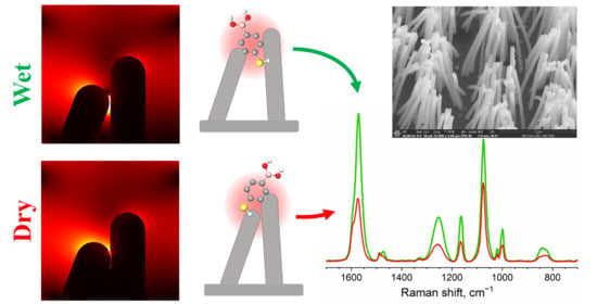
3. Results and Discussion

To the NW’s diameter optimization, the plasmon resonance in cylindrical two-dimensional (2D) NW under 785 nm laser excitation was simulated using electromagnetic PIC-code KARAT [35]. Longitudinal NW dimension was considered much larger than the transverse one. Figure 2 shows the dependence of the normalized electric field amplitude (E/E0) on single NW diameter at various distances from its surface; here, E is the amplitude of resulting electric field near the single NW, E0 is the amplitude of an incident laser electric field. To describe the electrodynamic properties of NWs, the Drude model was applied taking parameters for silver with laser excitation wavelength equal to 785 nm: a plasma frequency of 8.78 eV and damping constant of 0.02 eV [36]. Simulated E/E0 dependence on the Ag-NW diameter at various distances from its surface is present on Figure 2 and it is consistent with another study in which the field enhancement near the Ag-nanosphere is present [11]. It is seen that the maximum E/E0 was obtained at the Ag-NWs diameter ranging from 100 to 120 nm for all distances from the Ag-NW surface. Based on the obtained results, the diameter of the Ag-NWs was chosen to be 100 nm and the substrates were synthesized.
After the TM removal and following washing the substrates with the array of Ag-NWs, those substrates were left in distilled water. In this state, the Ag-NWs array remains uniformly distributed and maintains the structure of the initial TM. As distilled water was evaporated, Ag-NWs were leant together due to the capillary force, forming a hot spot between their tips and leading to the formation of a large-area ordered array of Ag-NWs bundles along the irradiation strips of the TM.
The substrate drying process and the characteristic leaned microstructure can be observed in real-time mode using an optical microscope. Figure 3 shows photos of the substrate surface with the Ag-NWs length of 12 μm in a wet form (Figure 3c) and after air-drying (Figure 3d). At the moment of complete drying of the substrate, surface tension will cause the Ag-NWs to lean towards their nearest neighbors, thus creating bundles. The length of the Ag-NWs was investigated by scanning electron microscopy (SEM) (Figure 3b). It also should be noticed that the morphology of the produced SERS totally reproduces the structure of the using TM (Figure 3a).
It was found that the largest length corresponds to bundles with a greater number of Ag-NWs due to their high elasticity. As a result, bundles consisting of dozens of densely leaned Ag-NWs formed without the breakaway of the Ag-NWs from the substrate. With a decrease in the length of the Ag-NWs, the number forming the bundle became smaller, and at a length in the range of 1.5–3 μm it was possible to observe single leaning Ag-NWs. When the length of the Ag-NWs was less than 1 μm, single standing Ag-NWs were observed on the surface without leaning. Based on the chemical compositions of studying substrates obtained from EDX analysis we can conclude that there is no influence of the copper layer and we end up with the Ag-NWs array on Ag-substrate.
To demonstrate the effect of various mechanisms on the amplification of the analyte SERS-signal, a series of samples with different Ag-NWs lengths were tested. The substrates were divided into three groups along the Ag-NWs length. Each group was split into “dry” and “wet” (Figure 4). “Dry” substrates were obtained by drying the substrate immediately after the TM removal and the following washing, while the “wet” ones were left in distilled water until the analyte exposure.
During the substrate drying, gap hot spots are formed in the spacing between the neighboring Ag-NWs. When the analyte is added to the “dry” substrate, the molecules are adsorbed along the entire Ag-NWs length, but can no longer be placed in the spacing between the neighboring Ag-NWs, since they were already leant before the analyte exposure. In the case of the “wet” substrate, the analyte molecules are also adsorbed on the entire Ag-NWs length. In the drying process, the Ag-NWs are leaning, and the molecules are trapped in the nanometric gap between the neighboring Ag-NWs, that is, in the gap hot spot region.
Figure 5 shows SERS-spectra of 10 μg/mL 4-MPBA adsorbed on the substrate with 1.1 μm Ag-NWs. All spectra were recorded six times from the different places of the substrate and then averaged, and the standard deviations are presented in Table 1. Based on the obtained spectra, we can conclude that on the “wet” substrates the probability that the analyte molecules will be in the gap hot spot region is greater than on the “dry” ones. It may be demonstrated by the spectrum intensity on the “wet” substrate, which is almost two times higher compared to the “dry” one. Moreover, the SERS-signal of 4-MPBA obtained on the substrate with the Ag-NWs array is more detailed compared to ordinary Raman of neat solid 4-MPBA presented in the paper [37]. The Raman spectrum of 10 mg/mL 4-MPBA also was recorded in our experiment and the most intense peak is presented in Figure 5. The Raman spectrum was recorded at the laser power of 120 mW and acquired in 10 s; a 785 nm laser was used. To lead the Raman spectrum to the same conditions as the SERS spectra, we assume that the intensity dependence on the laser power and the accumulation time is linear, so the Raman intensity was divided by 40.
Figure 6 shows the dependence of the SERS-spectra on the Ag-NWs length. Table 1 summarizes SERS intensities for 4-MPBA molecules adsorbed on Ag-NWs substrates with different length. With the length of the Ag-NWs in the range 3–12 μm (long nanowires), the signal intensity recorded on the “wet” substrate is 30% higher than from the “dry” one. With the length of the Ag-NWs from 1 to 3 μm (medium-sized nanowires), the signal intensity recorded on the “wet” substrate is 49% higher. On substrates with Ag-NWs with a length of less than 1 μm (short nanowires), there is a slight increase in intensity in the case of “wet” NWs (less 30%), since Ag-NWs hardly lean due to their too short length. Therefore, we deal with the simple array with non-leaning Ag-NWs, and the signal amplification is only due to the “lightning rod” effect.
The difference of SERS-signals caused by Ag-NWs length can be explained by the different leaning feature. In the case of “medium-sized NWs”, units of them are leaning partially along their length, so the Ag-NWs tips are parallel for the case of “dry” substrates. For the “wet” substrates, Ag-NWs tips are also parallel in the center of the bundle and few of them slightly diverge apart at the bundle edges, forming bigger spacing between their tips— in that spacing gap hot spots are presented by analogy with the colloidal solutions (Figure 7b). As it can be from the SEM images (Figure 7), exactly the “medium-sized NWs” are able to form vertical bundles, in which individual NWs fit tightly to each other, being located almost parallel.
When the Ag-NWs are “long”, dozens of the neighboring Ag-NWs tend to lean and the bundles become bigger with the increase in NWs length (Figure 7a), so that long NWs can no longer be positioned vertically (due to the combination of their mass and elastic properties) and they lean on each other, forming nano-contacts of the “tip-surface” type. As there is an insignificant difference in the Ag-NWs lengths along the substrate and some Ag-NWs are shorter than another, after the drying process the tip of one Ag-NW will be close to the side surface of its neighbor Ag-NW. For the “wet” substrates there will be a nanometer gap between the Ag-NW tip and the side surface of its neighbor, and for the “dry” ones there will be a point of contact between them. “Short NWs” are not elastic and the capillary force is not enough to lean them, and the increase of analyte SERS-signal is very slight (Figure 7c). The optimal aspect ratio is found to be 160.
To study the effect of the gap on the electric field enhancement the simulation was performed by code KARAT for the case of “long” and “medium-sized” Ag-NWs with a monochromatic incident laser wavelength of 785 nm. The laser pulse with linear (Ex, By) polarization propagated from the top down along z-direction (Figure 8), where the amplitude of the incident wave was taken as a unit of arbitrary units (a.u.). The normalized electric field amplitude E/E0 was obtained by the following procedure: the field amplitudes were calculated at all points of the computational area at each moment of time, then the ratio of the field amplitude at a certain point to the amplitude of the incident was found. A large E-field was found to be at the gap in the spacing between the adjacent Ag-NWs for the case of “wet” substrates, where Ag-NWs were not pre-leaned (Figure 8a,c).
The maximum E/E0 for the “long” Ag-NWs in the case of “wet” substrates was found to be 21.1 in the gap (order of 1 nm) between neighboring Ag-NWs (Figure 8a). For the case of “dry” substrates (NWs that are tightly leaning to each other), large E-field was found at the Ag-NWs touchpoint with the maximum E/E0 of 13.1 (Figure 8b).
For “long” Ag-NWs (the leaning angle is of 21 degrees) it was found out that the E/E0 depends on the gap size x (nm) according to the exponential scaling law, derived by fitting, and for x varying from 1 to 10 nm takes the following form:
E E 0 = 113 × e x + 4
We can conclude that E/E0 decay drastically with gap size x.
The case of the leaning geometry, demonstrated by the example of “medium-sized” NWs, is extremely promising. Depending on the angle between neighboring NWs, the E/E0 can be widely varied. This geometry leads to the concentration of electromagnetic energy in a narrowing gap between NWs and to the formation of a plasmon in it with several regions of electromagnetic field amplification, with a maximum E/E0 equals 74.5 for the case of “wet” substrate (the opening angle of the NWs in the calculated case is equal to 2 degrees). E/E0 is of 20 for the “dry” one in case of “medium-sized” NWs (Figure 8c,d). For the “wet” substrates the enhancement is strongly dependent on the geometry of leaning Ag-NWs (angle between them, length of the gap, etc.). The E/E0 obtained for “medium-sized” NWs can be significantly enhanced due to the incident field polarization.
As it is shown in [38] the SERS signal enhancement factor (EF) is connected with the field enhancement as (E/E0)4, considering its average over all illuminated molecules. Thus for the “medium-sized” NWs in case of the “wet” substrates EF is approximately equal to 3 × 10⁷.
We have also found the experimental value of EF from the ordinary Raman and SERS spectra of 4-MPBA on the substrate with “medium-sized” (length of 1.1 µm) NWs (see. Figure 5). The formula for the experimental EF includes the relation between SERS and Raman intensities as well as the relation between the number of molecules in the case of Raman and SERS. Here we compare data for most intensive spectral peak at ~1600 cm−1, which clearly resolved in all the spectra. As a result, we have found the EF for the “wet” substrate as high as 7 × 10⁸. We attribute the difference between experimental and theoretical EF to the specific distribution (adsorption) of 4-MPBA molecules on the SERS-substrate with developed relief.

4. Conclusions

In summary, we report a simple strategy for the fabrication procedure of the SERS-active substrates with the array of metal nanowires (NWs) using a template-assisted electrodeposition method with commercial tracking membranes (TM). It is possible to choose the proper TM with certain diameter of NWs and its surface density, while template synthesis technology allows varying NWs length. Owing to different length, NWs tend to lean forming bundles with different character of gap hot spots. According to model calculations of electromagnetic field distribution, there is large field enhancement due to the presence of gap hot spots in the spacing between neighboring NWs tips. For different leaning geometries, the E-field enhancement was found to be distributed in the range up to 70 and even more. It corresponds to the estimated SERS enhancement factor up to ~107.
The applicability of this approach was confirmed by the experiments with Ag-NWs substrates with different NWs length (from 0.6 to 7.7 µm). The optimal NWs length was found as high as 1.6 µm in order to obtain maximum SERS spectra intensities. This length corresponds to NWs leaning only by its tips that leads to more effective hot spot formation.
Also, SERS spectra have been measured for 4-MPBA on two different types of substrates: “dry” (analyte was added after substrate drying) and “wet” (analyte was added before drying). The intensity of the SERS-signal recorded on the “wet” and “dry” substrates depends a lot of NWs length. For medium-sized NWs (length from 1 to 3 μm) the intensity on the “wet” substrate is 49% higher than on “dry” because of the analyte distribution. Analyte molecules caught between NWs tips are affected by high local electromagnetic field, result in higher SERS signal intensity compared to molecules adsorbed on the top of NWs tips. Finally, for optimal NWs length we achieved an enhancement factor up to ~108 for 4-MPBA on the “wet” substrates.
We assume that our substrates are cost-effective and easy to manufacture. With the proper (optimized) parameters such substrates can be useful for numerous applications where the ability to detect trace levels of chemicals is required.

Author Contributions

Conceptualization, E.P.K., V.P.T. and S.N.A.; Data curation, E.P.K.; Formal analysis, S.A.B., N.L.N., S.N.P., Y.V.G. and A.V.N.; Funding acquisition, Y.V.G. and A.V.N.; Investigation, E.P.K.; Methodology, S.A.B., N.L.N., V.P.T. and S.N.A.; Project administration, E.P.K.; Resources, E.P.K., N.L.N., S.N.P., V.P.T., S.N.A., Y.V.G. and A.V.N.; Software, S.N.P., V.P.T. and S.N.A.; Supervision, E.P.K.; Writing—original draft, E.P.K., V.P.T. and S.N.A.; Writing—review & editing, S.A.B., N.L.N., S.N.P., Y.V.G. and A.V.N. All authors have read and agreed to the published version of the manuscript.

Funding

This research was funded by the Ministry of Education of Russia and Ministry of Science and High Education of Russia (project State number AAAA-A20-120061890084-9 “Physics of nanostructured materials: fundamental research and applications in materials science, nanotechnology and photonics” and by the Russian Foundation for Basic Research (RFBR), project number 18-29-12099. The experimental technique for spectral analysis of complex organic macromolecules is developed for the purposes of RFBR project number 20-03-00923. SEM images using the equipment of the Center for Collective Use of the Federal Research Center “Crystallography and Photonics of the Russian Academy of Sciences”.

Data Availability Statement

The data presented in this study are available on request from the corresponding author.

Conflicts of Interest

The authors declare no conflict of interest.

References

  1. Radziuk, D.; Moehwald, H. Prospects for plasmonic hot spots in single molecule SERS towards the chemical imaging of live cells. Phys. Chem. Chem. Phys. 2015, 17, 21072–21093. [Google Scholar] [CrossRef] [PubMed] [Green Version]
  2. Etchegoin, P.G.; Le Ru, E.C. A perspective on single molecule SERS: Current status and future challenges. Phys. Chem. Chem. Phys. 2008, 10, 6079–6089. [Google Scholar] [CrossRef] [PubMed]
  3. Anger, P.; Bharadwaj, P.; Novotny, L. Enhancement and quenching of single-molecule fluorescence. Phys. Rev. Lett. 2006, 96, 113002. [Google Scholar] [CrossRef] [PubMed] [Green Version]
  4. Tian, M.; Wang, J.; Kurtz, J.; Mallouk, T.E.; Chan, M.H. Electrochemical Growth of Single-Crystal Metal Nanowires via a Two-Dimensional Nucleation and Growth Mechanism. Nano. Lett. 2003, 3, 919–923. [Google Scholar] [CrossRef]
  5. Zhang, W.; Caldarola, M.; Lu, X.; Orrit, M. Plasmonic Enhancement of Two-Photon-Excited Luminescence of Single Quantum Dots by Individual Gold Nanorods. Acs Photonics 2018, 5, 2960–2968. [Google Scholar] [CrossRef]
  6. Naumova, N.L.; Vasil’eva, I.A.; Osad’ko, I.S.; Naumov, A.V. Study of Vibronic Interactions in Impurity Centers by Conjugate Fluorescence and Absorption Spectra with a Poorly Resolved Vibrational Structure. Opt. Spectrosc. 2005, 98, 535–542. [Google Scholar] [CrossRef]
  7. Naumov, A.V. Low-temperature spectroscopy of organic molecules in solid matrices: From the Shpol’skii effect to laser luminescent spectromicroscopy for all effectively emitting single molecules. Physics-Uspekhi 2013, 56, 605–622. [Google Scholar] [CrossRef]
  8. Karimullin, K.R.; Arzhanov, A.I.; Eremchev, I.Y.; Kulnitskiy, B.A.; Surovtsev, N.V.; Naumov, A.V. Combined photon-echo, luminescence and Raman spectroscopies of layered ensembles of colloidal quantum dots. Laser Phys. 2019, 29, 124009. [Google Scholar] [CrossRef]
  9. Naumov, A.V.; Gorshelev, A.A.; Gladush, M.G.; Anikushina, T.A.; Golovanova, A.V.; Kohler, J.; Kador, L. Micro-Refractometry and Local-Field Mapping with Single Molecules. Nano. Lett. 2018, 18, 6129–6134. [Google Scholar] [CrossRef]
  10. Gladush, M.G.; Anikushina, T.A.; Gorshelev, A.A.; Plakhotnik, T.V.; Naumov, A.V. Dispersion of Lifetimes of Excited States of Single Molecules in Organic Matrices at Ultralow Temperatures. J. Exp. Theor. Phys. 2019, 128, 655–663. [Google Scholar] [CrossRef]
  11. Vladimirova, Y.V.; Klimov, V.V.; Pastukhov, V.M.; Zadkov, V.N. Modification of two-level-atom resonance fluorescence near a plasmonic nanostructure. Phys. Rev. A 2012, 85, 85. [Google Scholar] [CrossRef]
  12. Klimov, V. Nanoplasmonics; Pan Stanford: Boca Raton, FL, USA, 2014. [Google Scholar]
  13. Kuttner, C. Plasmonics in Sensing: From Colorimetry to SERS Analytics. In Plasmonics; IntechOpen: London, UK, 2018. [Google Scholar] [CrossRef] [Green Version]
  14. Škantárová, L.; Oriňák, A.; Oriňáková, R.; Lofaj, F. 4-Aminothiophenol Strong SERS Signal Enhancement at Electrodeposited Silver Surface. Nano-Micro Lett. 2012, 4, 184–188. [Google Scholar] [CrossRef] [Green Version]
  15. Drachev, V.P.; Thoreson, M.D.; Nashine, V.; Khaliullin, E.N.; Ben-Amotz, D.; Davisson, V.J.; Shalaev, V.M. Adaptive silver films for surface-enhanced Raman spectroscopy of biomolecules. J. Raman Spectrosc. 2005, 36, 648–656. [Google Scholar] [CrossRef] [Green Version]
  16. Matsukovich, A.S.; Nalivaiko, O.Y.; Chizh, K.V.; Gaponenko, S.V. Raman Scattering Enhancement Using Au/SiGe and Au/Ge Nanostructures. J. Appl. Spectrosc. 2019, 86, 72–75. [Google Scholar] [CrossRef]
  17. Lepeshov, S.I.; Krasnok, A.E.; Belov, P.A.; Miroshnichenko, A.E. Hybrid nanophotonics. Physics-Uspekhi 2018, 61, 1035–1050. [Google Scholar] [CrossRef] [Green Version]
  18. Kozhina, E.P.; Bedin, S.A.; Razumovskaya, I.V.; Zalygin, A.V. Synthesizing of the SERS-active substrates. J. Phys. Conf. Ser. 2019, 1283. [Google Scholar] [CrossRef] [Green Version]
  19. Ermushev, A.V.; McHedlishvili, B.V.; Oleĭnikov, V.A.; Petukhov, A.V. Surface enhancement of local optical fields and the lightning-rod effect. Quantum Electron. 1993, 23, 435–440. [Google Scholar] [CrossRef]
  20. Oleinikov, V.A.P.; Mchedlishvili, B.V. Track etched membrane in the template synthesis of SERS-active nanostructure. Seriya Krit Tekhnologii Membrany 2004, 24, 17–28. [Google Scholar]
  21. Le Ru, E.C.; Etchegoin, P.G. Quantifying SERS enhancements. Mrs Bull. 2013, 38, 631–640. [Google Scholar] [CrossRef]
  22. Kumar, C.S.S.R. Raman Spectroscopy for Nanomaterials Characterization; Springer Science & Business Media: Medford, MA, USA, 2012. [Google Scholar] [CrossRef]
  23. Kozhina, E.P.; Andreev, S.N.; Tarakanov, V.P.; Bedin, S.A.; Doludenko, I.M.; Naumov, A.V. Study of local fields of dendritic nanostructures in hot spots on substrates for giant Raman scattering fabricated by template synthesis. Bull. Russ. Acad. Sci. Phys. 2020, 84, 4. [Google Scholar] [CrossRef]
  24. Schmidt, M.S.; Hubner, J.; Boisen, A. Large area fabrication of leaning silicon nanopillars for surface enhanced Raman spectroscopy. Adv. Mater. 2012, 24, OP11-18. [Google Scholar] [CrossRef] [PubMed]
  25. Flerov, G.N.; Barashenkov, V.S. Practical applications of heavy ion beams. Sov. Phys. Uspekhi 1975, 17, 783–793. [Google Scholar] [CrossRef]
  26. Spohr, R. Ion Tracks and Microtechnology; Bethge, K., Ed.; Vieweg Bertelsmann Publishing Group International: Gütersloh, Germany, 1990. [Google Scholar] [CrossRef]
  27. Apel, P. Track etching technique in membrane technology. Radiat. Meas. 2001, 34, 559–566. [Google Scholar] [CrossRef]
  28. Martin, C.R. Membrane-Based Synthesis of Nanomaterials. Chem. Mater. 1996, 8, 1739–1746. [Google Scholar] [CrossRef]
  29. Martin, C.R. Nanomaterials: A membrane-based synthetic approach. Science 1994, 266, 1961–1966. [Google Scholar] [CrossRef] [PubMed]
  30. Schönenberger, C.; van der Zande, B.M.I.; Fokkink, L.G.J.; Henny, M.; Schmid, C.; Krüger, M.; Bachtold, A.; Huber, R.; Birk, H.; Staufer, U. Template Synthesis of Nanowires in Porous Polycarbonate Membranes: Electrochemistry and Morphology. J. Phys. Chem. B 1997, 101, 5497–5505. [Google Scholar] [CrossRef]
  31. Zoski, C.G. (Ed.) Handbook of Electrochemistry; Elsevier: Amsterdam, The Netherlands, 2007; p. 934. [Google Scholar] [CrossRef]
  32. Bedin, S.A.; Rybalko, O.G.; Polyakov, N.B.; Zagorskii, D.L.; Razumovskaya, A.V.; Bondarenko, G.G.; Oleinikov, V.A. Metal micro- and nanowires fabricated by matrix synthesis and their application in mass spectrometry. Inorg. Mater. Appl. Res. 2010, 1, 359–364. [Google Scholar] [CrossRef]
  33. Zhu, C.; Meng, G.; Zheng, P.; Huang, Q.; Li, Z.; Hu, X.; Wang, X.; Huang, Z.; Li, F.; Wu, N. A Hierarchically Ordered Array of Silver-Nanorod Bundles for Surface-Enhanced Raman Scattering Detection of Phenolic Pollutants. Adv. Mater. 2016, 28, 4871–4876. [Google Scholar] [CrossRef]
  34. Lee, S.J.; Morrill, A.R.; Moskovits, M. Hot spots in silver nanowire bundles for surface-enhanced Raman spectroscopy. J. Am. Chem. Soc. 2006, 128, 2200–2201. [Google Scholar] [CrossRef]
  35. Tarakanov, V.P. Code KARAT in simulations of power microwave sources including Cherenkov plasma devices, vircators, orotron, E-field sensor, calorimeter etc. EPJ Web Conf. 2017, 149, 04024. [Google Scholar] [CrossRef]
  36. Johnson, P.B.; Christy, R.W. Optical Constants of the Noble Metals. Phys. Rev. B 1972, 6, 4370–4379. [Google Scholar] [CrossRef]
  37. Li, S.; Zhou, Q.; Chu, W.; Zhao, W.; Zheng, J. Surface-enhanced Raman scattering behaviour of 4-mercaptophenyl boronic acid on assembled silver nanoparticles. Phys. Chem. Chem. Phys. 2015, 17, 17638–17645. [Google Scholar] [CrossRef] [PubMed]
  38. Langer, J.; Jimenez de Aberasturi, D.; Aizpurua, J.; Alvarez-Puebla, R.A.; Auguie, B.; Baumberg, J.J.; Bazan, G.C.; Bell, S.E.J.; Boisen, A.; Brolo, A.G.; et al. Present and Future of Surface-Enhanced Raman Scattering. ACS Nano 2020, 14, 28–117. [Google Scholar] [CrossRef] [PubMed] [Green Version]
Figure 1. Scheme of the template synthesis of silver NWs: (a) initial TM, (b) formation of a conductive layer, (c) electrochemical deposition of metal into the pores of TM, (d) TM removal.
Applsci 11 01375 g001
Figure 2. Simulated dependence of the normalized electric field amplitude (E/E0) on the Ag-NW diameter at various distances from its surface: (1) 2.5 nm; (2) 5 nm; (3) 10 nm.
Applsci 11 01375 g002
Figure 3. SEM top view of the TM (a) and the surface of the substrate with an Ag-NWs bundles array with an Ag-NWs diameter of 100 nm and their length of 12 μm. SEM top view of the Ag-NWs bundles array (b). Photos of the substrate are made by optical microscope (c) when it is in a wet state, (d) of the same area after drying.
Applsci 11 01375 g003
Figure 4. Schematic procedure for the gap hot spots formation on the array of Ag-NWs bundles in case of the «dry» and «wet» SERS-substrates. (1) The array of Ag-NWs on a metal substrate is being in the water after etching of TM. (2a) as distilled water was evaporated, Ag-NWs were leant together by its tips due to the capillary force. (3a) An analyte was added on the already formed Ag-NWs bundles, so the analyte molecules could not be in the spacing between neighboring Ag-NWs tips and consequently in the gap hot spot region (4a). (2b) an analyte was added on wet substrates. (3b) Molecules of an analyte were adsorbed on the entire length of the Ag-NWs, and during the Ag-NWs leaning, the molecules were trapped in the gap hot spot region.
Applsci 11 01375 g004
Figure 5. SERS-spectra of 10 μg/mL 4-MPBA adsorbed on the “wet” (green dash line) and “dry” (red dash-dot line) substrates with 1.1 μm Ag-NWs. For comparison the ordinary Raman spectrum of 4-MPBA is shown (blue solid line): brightest Raman spectral peak at ~1600 cm−1 (in enlarged scale in the dashed circle insert). On the insert chemical structure of the analyte molecule is shown.
Applsci 11 01375 g005
Figure 6. SERS-spectra of 10 μg/mL 4-MPBA adsorbed on the “dry” and “wet” substrates with Ag-NWs with a diameter of 100 nm collected in 1571 cm−1.
Applsci 11 01375 g006
Figure 7. Feature of the leaning of the 100 nm diameter Ag-NWs, depending on their length. (a) shows that sufficiently long NWs form the bundle, while so-called “middle-sized” NWs form the point contact between their tips (b). NWs with the length of fewer than 1 μm are not leaning due to its short length (c).
Applsci 11 01375 g007
Figure 8. E-field distribution in the nanometric gap between two Ag-NWs for two types of substrates: (a) “wet” and (b) “dry” substrates with “long” Ag-NWs; (c) “wet” and (d) “dry” substrates with “medium-sized” Ag-NWs.
Applsci 11 01375 g008aApplsci 11 01375 g008b
Table 1. Summary of the investigated 4-MPBA intensities adsorbed on different types of substrates differs by Ag-NWs length collected in 1571 cm−1.
Substrates TypeLength of Ag-NWs, µmAspect Ratio (Length/Diameter)Type of SubstrateMean Intensity × 103, a.u.Standard Deviation × 103, a.u.The Ratio of Intensities Obtained on the “wet” and “dry” Substrates
Short NWs0.660Wet1.670.741.30
Dry1.280.29
0.770Wet3.770.921.17
Dry3.230.78
Medium-sized NWs1.1110Wet8.980.642.35
Dry3.820.52
1.6160Wet20.181.371.46
Dry13.801.12
2.1210Wet12.520.762.03
Dry6.170.82
2.5250Wet8.910.371.44
Dry6.430.39
Long NWs5500Wet6.800.311.97
Dry4.990.34
7.7770Wet5.570.831.12
Dry3.450.91
Publisher’s Note: MDPI stays neutral with regard to jurisdictional claims in published maps and institutional affiliations.

