
Design and Implementation of New Coplanar FA Circuits without NOT Gate and Based on Quantum-Dot Cellular Automata Technology


Abstract
:1. Introduction
2. Background
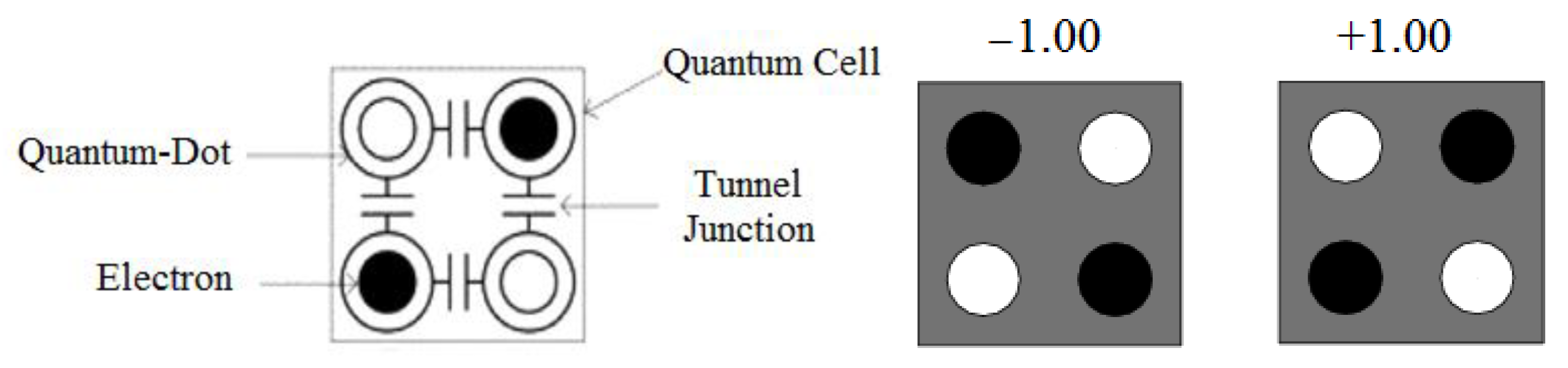
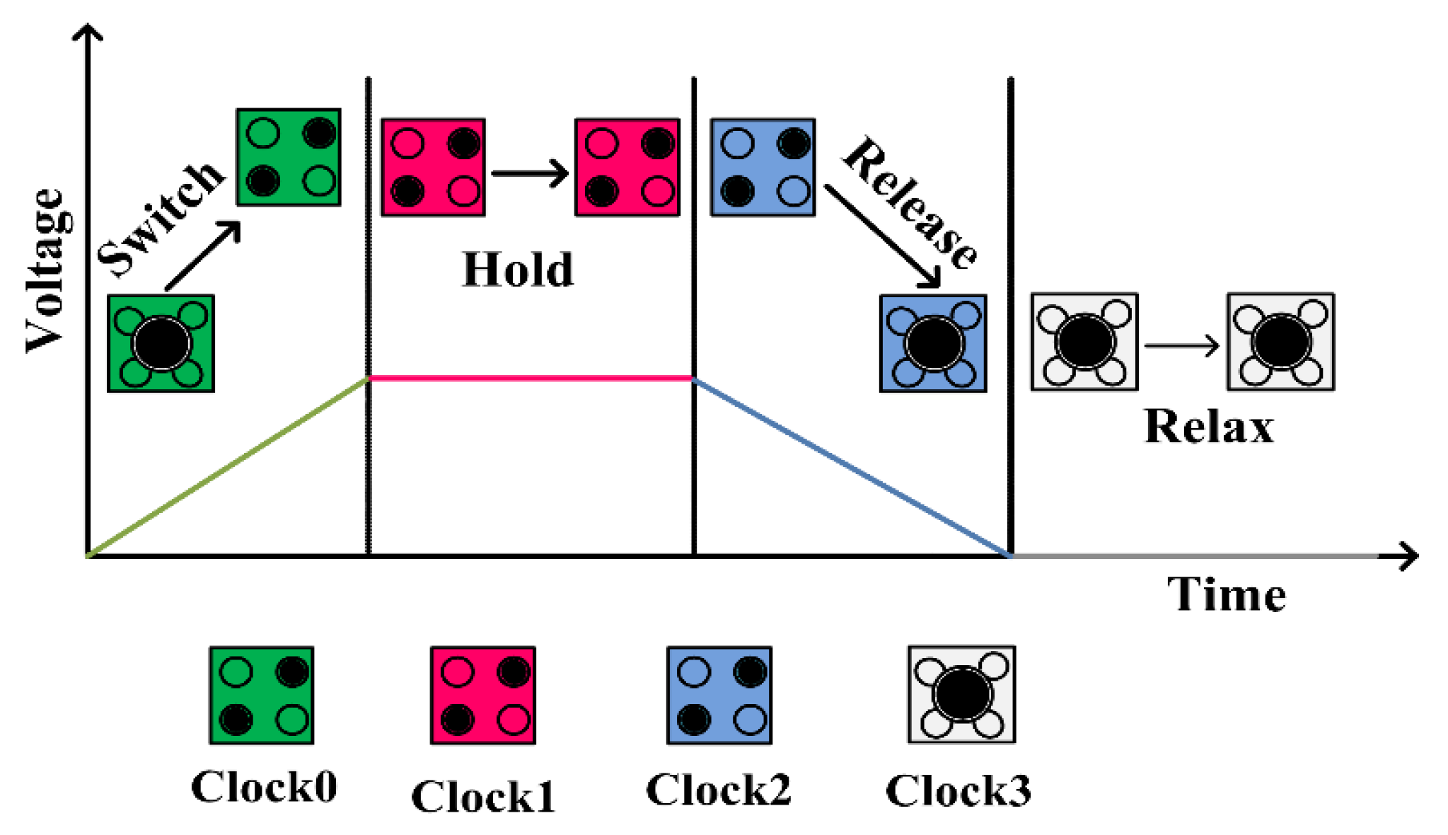
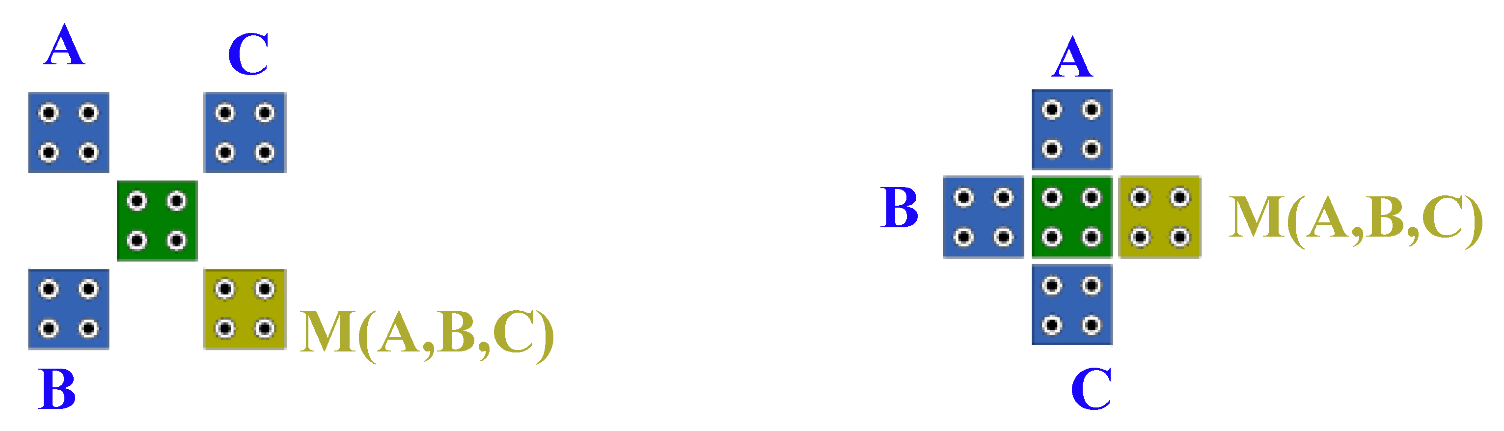
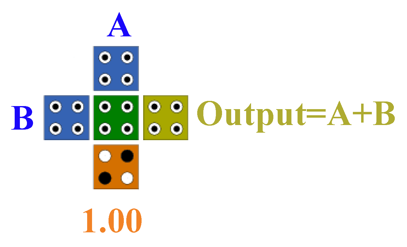
The QCA Basics
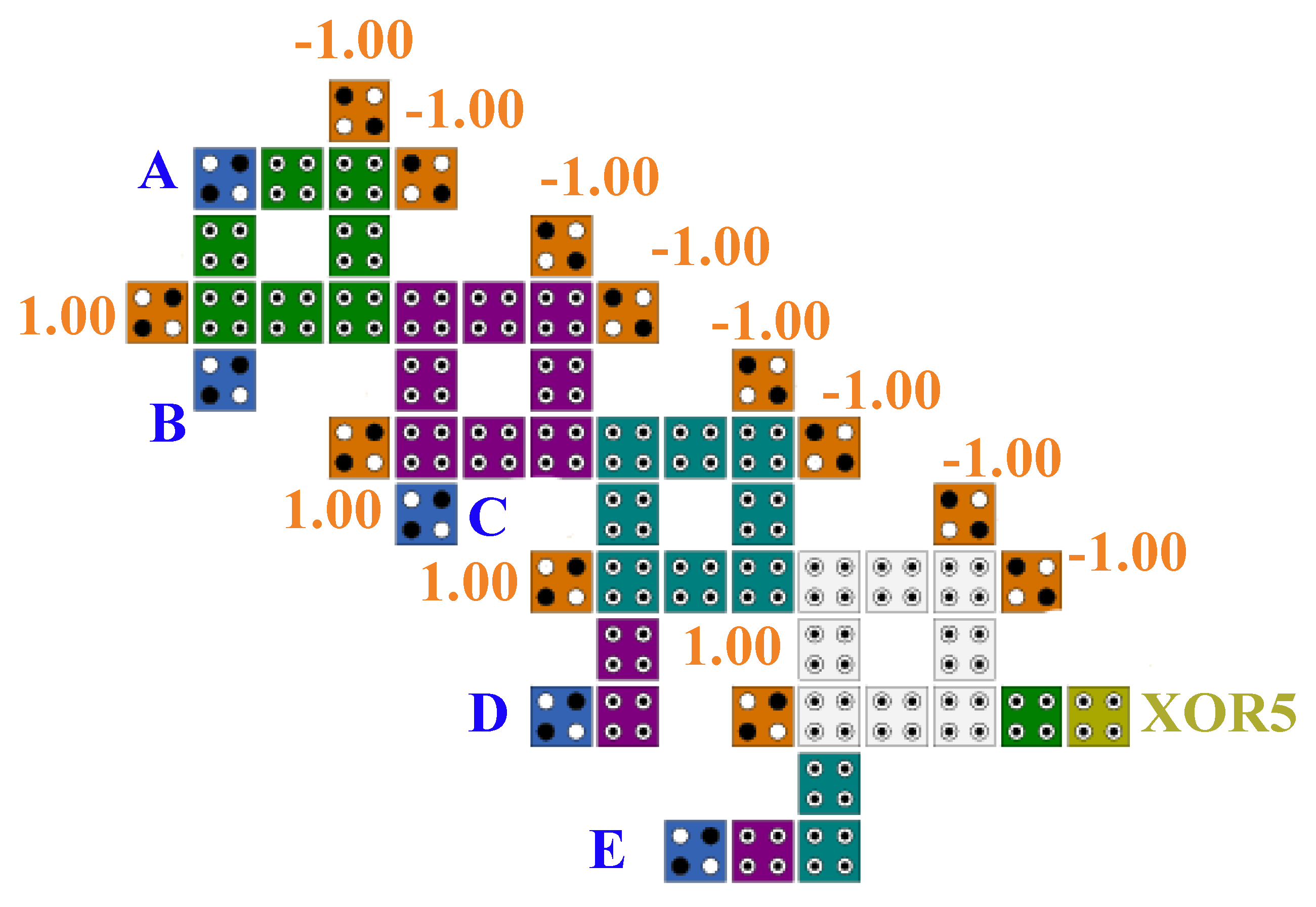
3. The Proposed Circuits
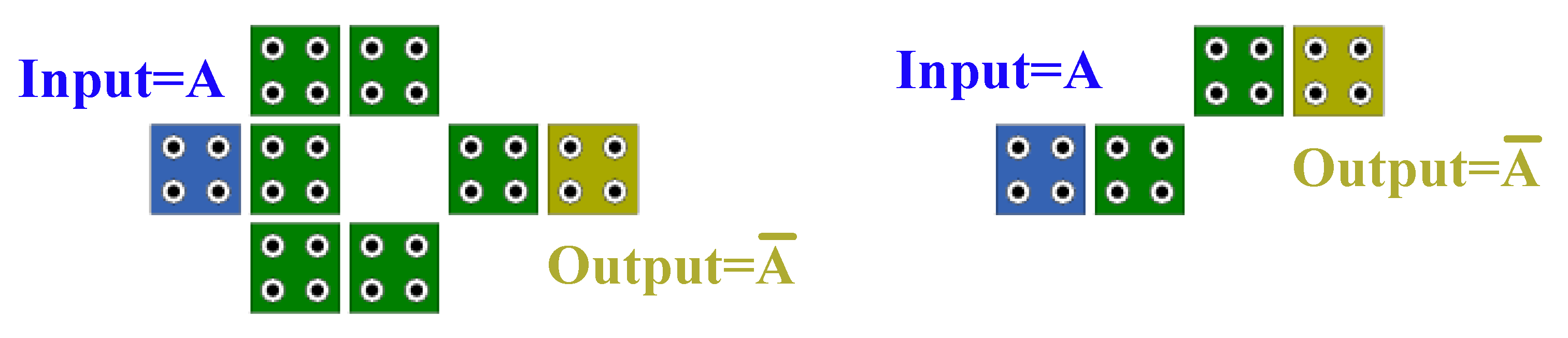
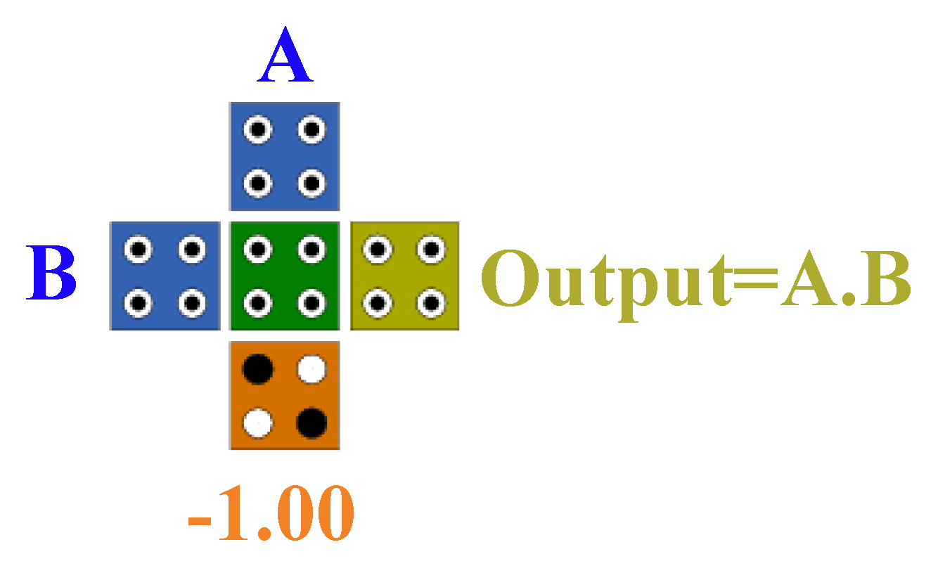
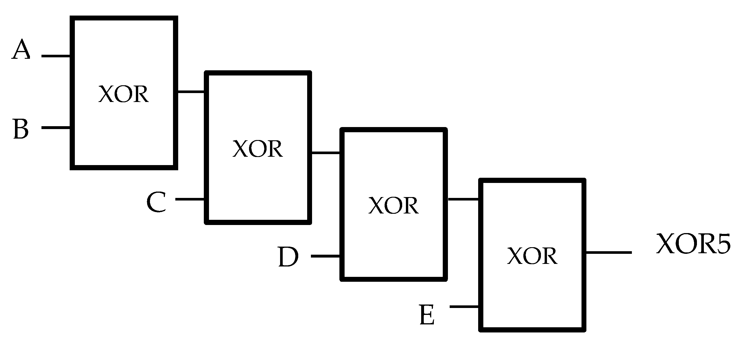
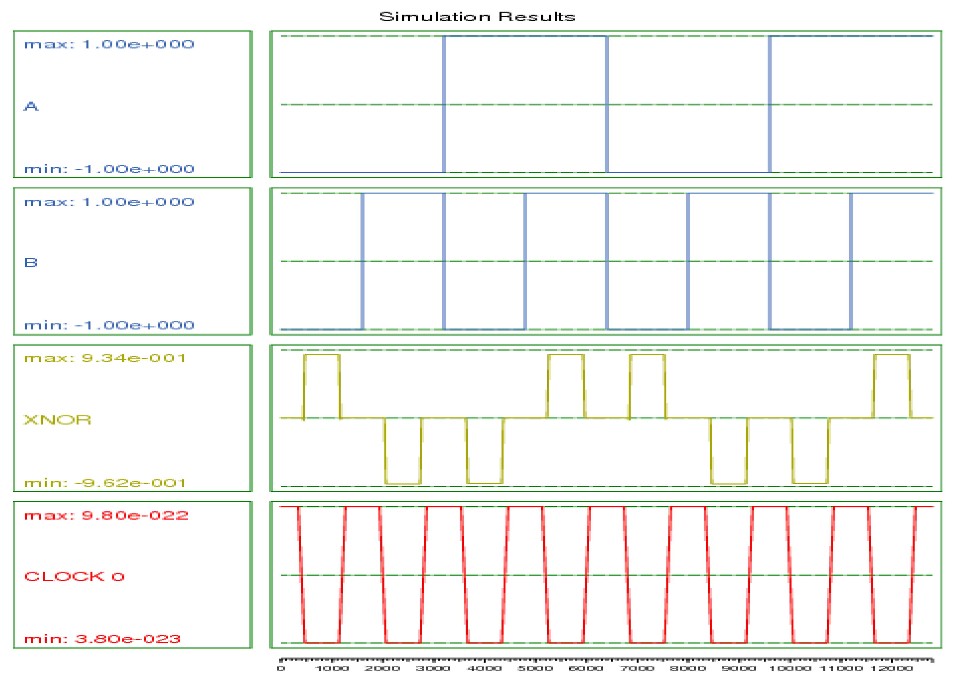
3.1. The XOR Gate Design
- -
- Reduced number of cells consumed;
- -
- Reduced consumption area;
- -
- Reduced cost function;
- -
- Less delay;
- -
- No use of NOT gates;
- -
- No use of crossovers;
- -
- No use of rotary cells (45-degree cells).
3.2. The XNOR Gate Design
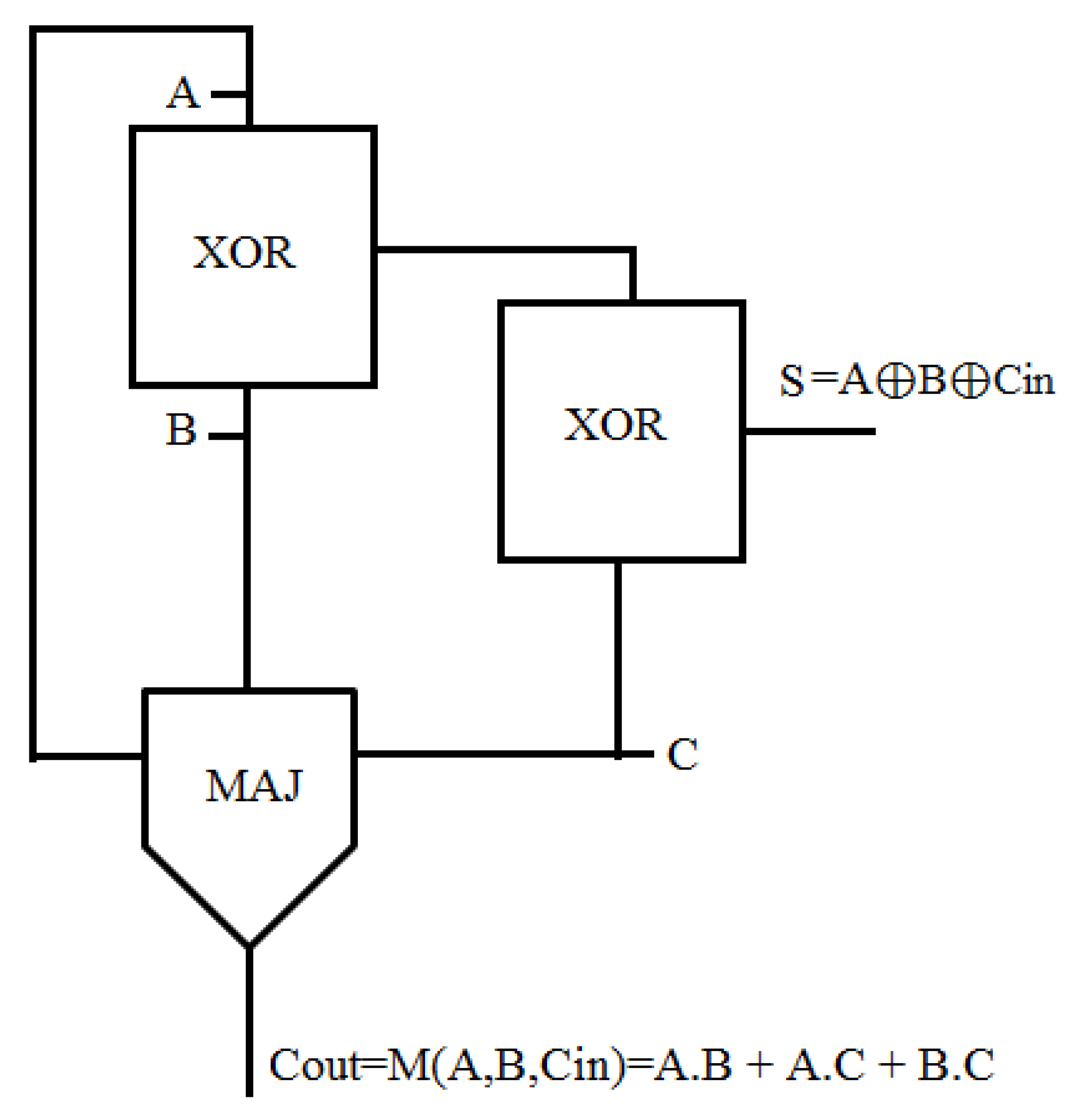
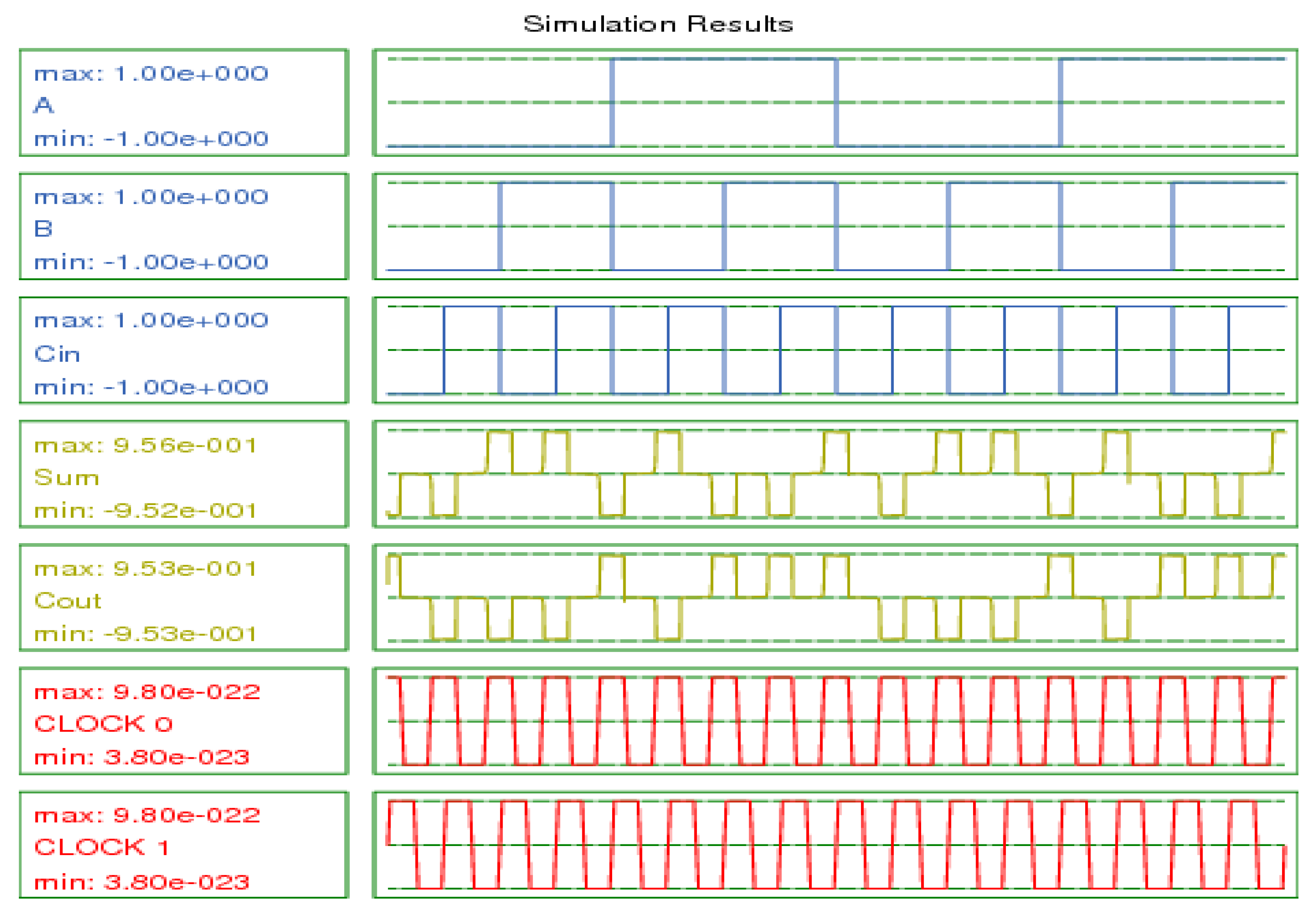
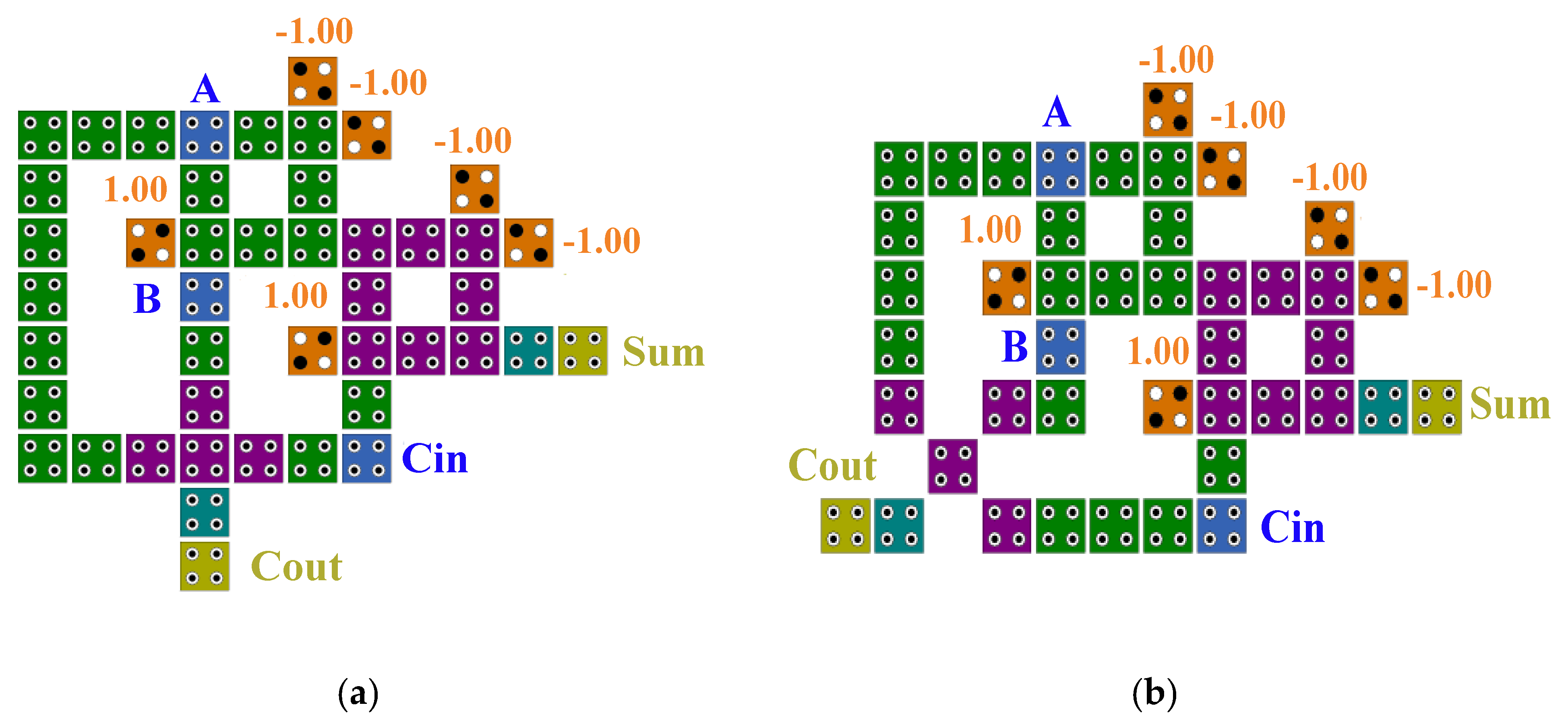
3.3. The Full Adder (FA) Circuits’ Design
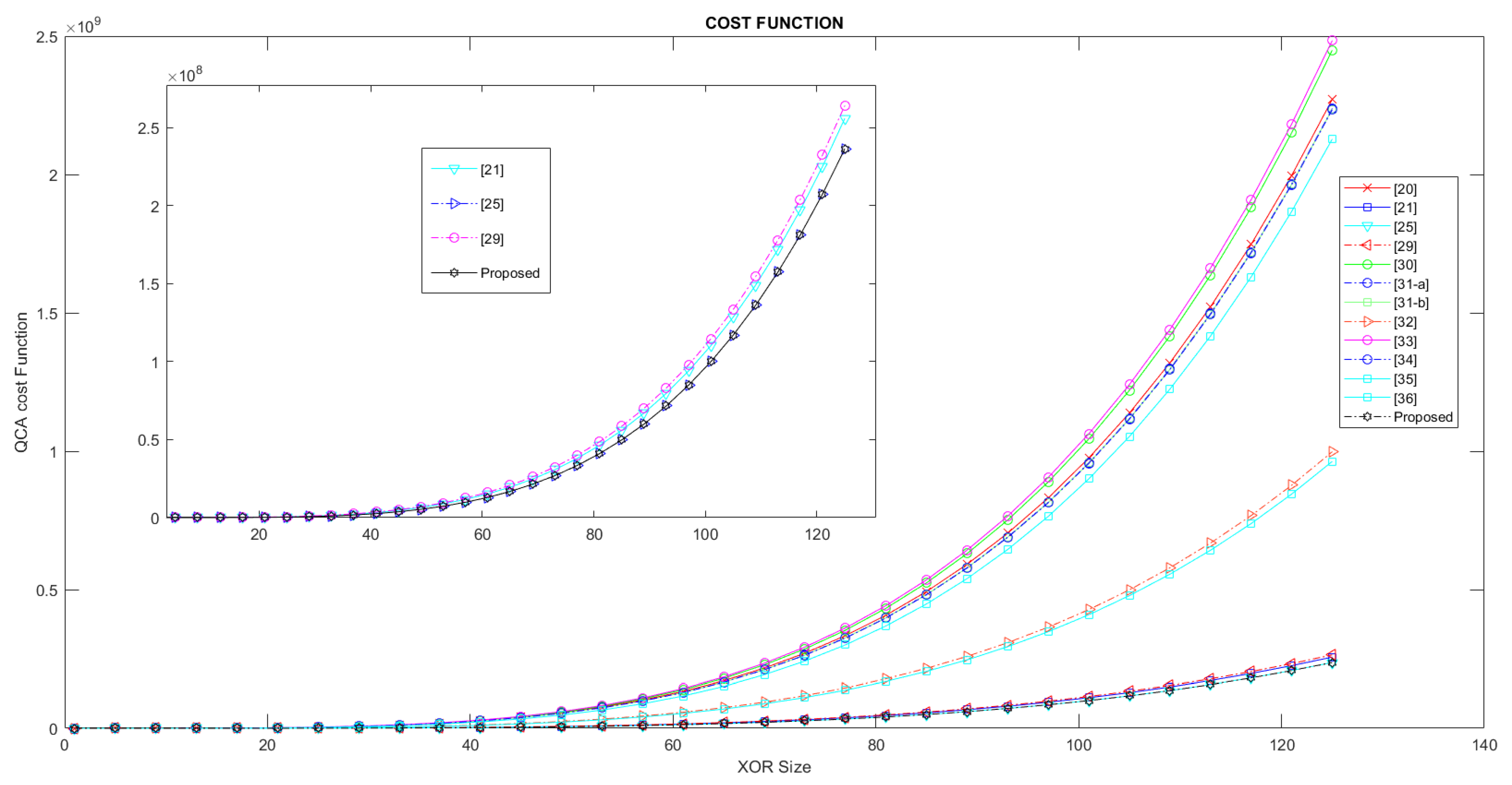
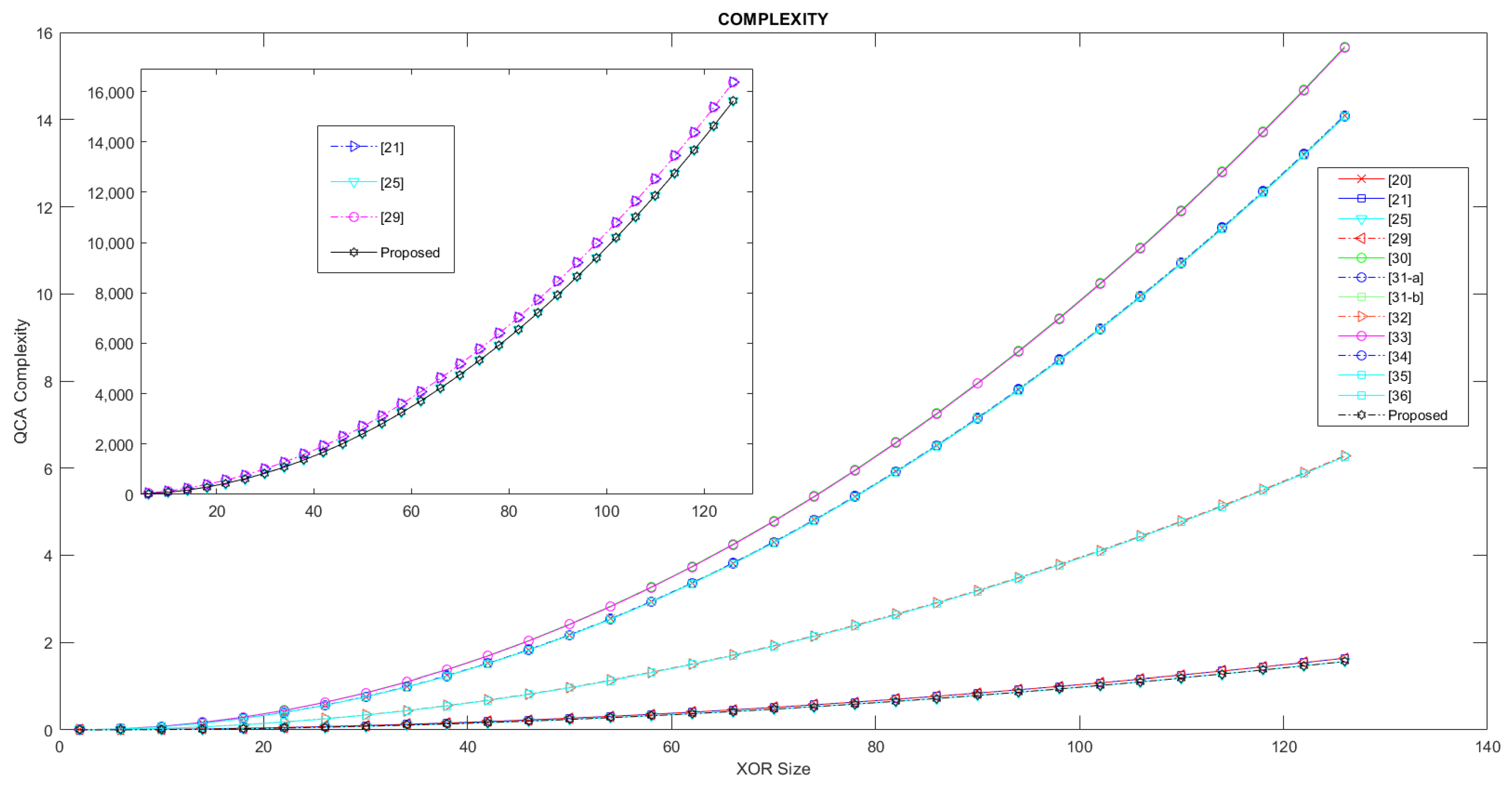
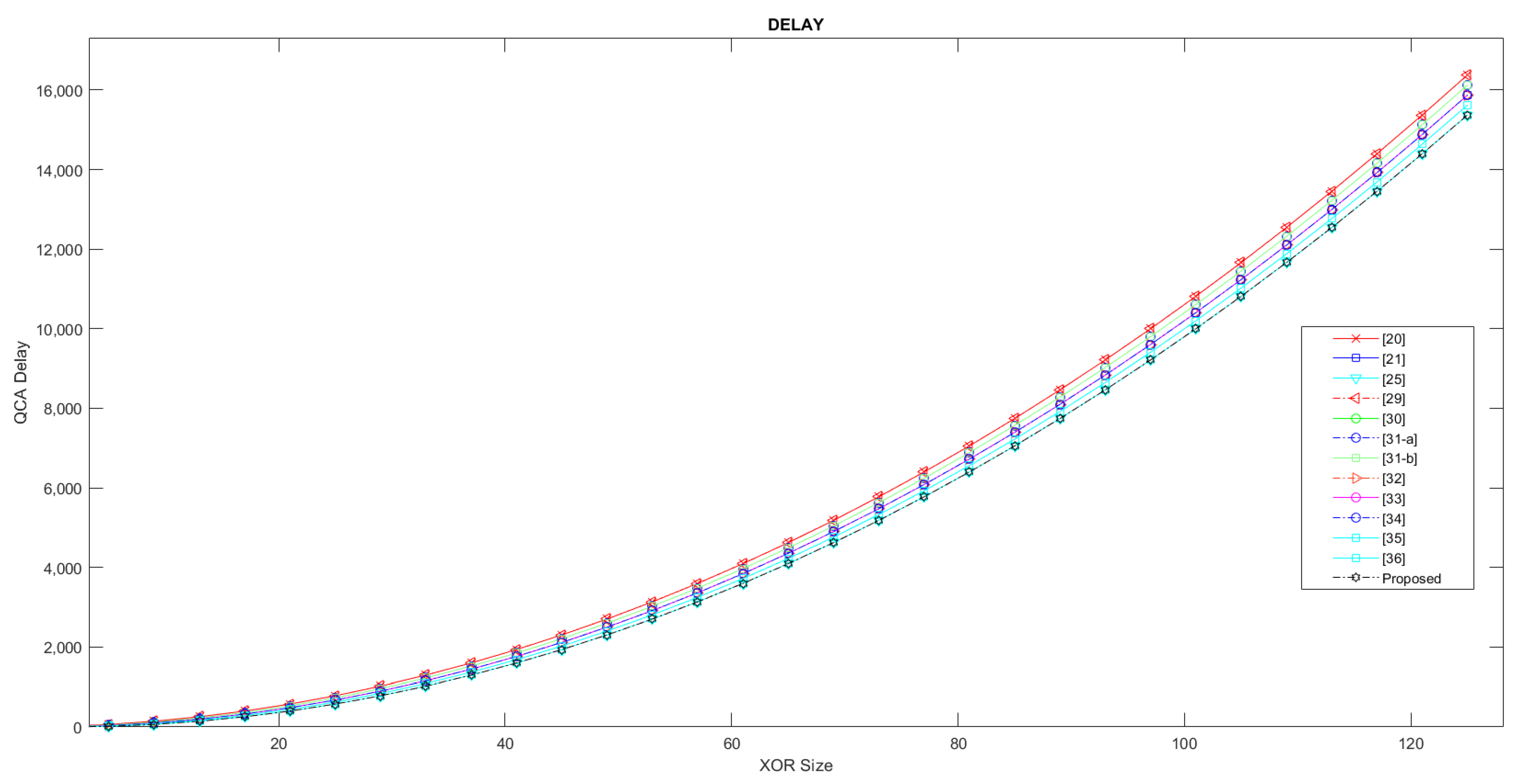
4. Performance Evaluation
5. Power Delay Product (PDP) Analysis
6. Conclusions
Author Contributions
Funding
Institutional Review Board Statement
Informed Consent Statement
Data Availability Statement
Conflicts of Interest
References
- Roohi, A.; DeMara, R.F.; Khoshavi, N. Design and evaluation of an ultra-area-efficient fault-tolerant QCA full adder. Microelectron. J. 2015, 46, 531–542. [Google Scholar] [CrossRef]
- Babaie, S.; Sadoghifar, A.; Bahar, A.N. Design of an efficient multilayer arithmetic logic unit in quantum-dot cellular automata (QCA). IEEE Trans. Circuits Syst. II Express Briefs 2018, 66, 963–967. [Google Scholar] [CrossRef]
- Liu, W.; Swartzlander, E.E., Jr.; O’Neill, M. Design of Semiconductor QCA Systems; Artech House: Norwood, MA, USA, 2013. [Google Scholar]
- Macucci, M. Quantum Cellular Automata; Imperial College Press: London, UK, 2006. [Google Scholar]
- Walus, K.; Dysart, T.J.; Jullien, G.A.; Budiman, R. A QCADesigner: A rapid design and simulation tool for quantum-dot cellular automata. IEEE Trans. Nanotechnol. 2004, 3, 26–31. [Google Scholar] [CrossRef]
- Teodosio, T.; Sousa, L. QCA-LG: A tool for the automatic layout generation of QCA combinational circuits. In Proceedings of the IEEE Norchip, Aalborg, Denmark, 19–20 November 2007; pp. 1–5. [Google Scholar]
- Swartzlander, E.E.; Cho, H.; Kong, I.; Kim, S.W. Computer arithmetic implemented with QCA: A progress report. In Proceedings of the Forty Fourth Asilomar Conference on Signals, Systems and Computers, Pacific Grove, CA, USA, 4–7 November 2010. [Google Scholar]
- Vahabi, M.; Lyakhov, P.; Bahar, A.N. Design and Implementation of Novel Efficient Full Adder/Subtractor Circuits Based on Quantum-Dot Cellular Automata Technology. Appl. Sci. 2021, 11, 8717. [Google Scholar] [CrossRef]
- Tougaw, P.D.; Lent, C.S. Logical devices implemented using quantum cellular automata. J. Appl. Phys. 1994, 75, 1818–1825. [Google Scholar] [CrossRef]
- Cho, H.; Swartzlander, E.E. Adder designs and analyses for quantum-dot cellular automata. IEEE Trans. Nanotechnol. 2007, 6, 374–383. [Google Scholar] [CrossRef]
- Huang, J.; Momenzadeh, M.; Tahoori, M.B.; Lombardi, F. Design and characterization of an and-or-inverter (AOI) gate for QCA implementation. In Proceedings of the 14th ACM Great Lakes Symposium on VLSI 2004, Boston, MA, USA, 26–28 April 2004; pp. 426–429. [Google Scholar]
- Shin, S.-H.; Jeon, J.-C.; Yoo, K.-Y. Wire-crossing technique on quantum-dot cellular automata. In Proceedings of the NGCIT2013: 2nd International Conference on Next Generation Computer and Information Technology, Las Vegas, NV, USA, 15–17 April 2013; Volume 27, pp. 52–57. [Google Scholar]
- Lent, C.S.; Tougaw, P.D.; Porod, W. Quantum cellular automata: The physics of computing with arrays of quantum dot molecules. In Proceedings of the PhysComp 94: Workshop on Physics and Computing, Dallas, TX, USA, 17–20 November 1994; pp. 5–13. [Google Scholar]
- Frost, S.E.; Rodrigues, A.F.; Janiszewski, A.W.; Rausch, R.T.; Kogge, P.M. Memory in motion: A study of storage structures in QCA. In Proceedings of the First Workshop on Non-Silicon Computing, Cambridge, MA, USA, 3 February 2002. [Google Scholar]
- Wang, W.; Walus, K.; Jullien, G.A. Quantum-dot cellular automata adders. In Proceedings of the 2003 Third IEEE Conference on Nanotechnology, San Francisco, CA, USA, 12–14 August 2003; pp. 461–464. [Google Scholar]
- Beigh, M.R.; Mustafa, M.; Ahmad, F. Performance evaluation of efficient XOR structures in quantum-dot cellular automata (QCA). Sci. Res. Circuits Syst. 2013, 4, 29850. [Google Scholar] [CrossRef] [Green Version]
- Modi, S.; Tomar, A.S. Logic gate implementations for quantum dot cellular automata. In Proceedings of the 2010 International Conference on IEEE Computational Intelligence and Communication Networks (CICN), Bhopal, India, 26–28 November 2010. [Google Scholar]
- Liu, W.; Lu, L.; O’Neill, M.; Swartzlander, E.E. A first step toward cost functions for quantum-dot cellular automata designs. IEEE Trans. Nanotechnol. 2014, 13, 476–487. [Google Scholar]
- Chabi, A.M.; Sayedsalehi, S.; Angizi, S.; Navi, K. Efficient QCA exclusive-or and multiplexer circuits based on a nanoelectronic-compatible designing approach. Int. Sch. Res. Not. 2014, 2014, 63967. [Google Scholar] [CrossRef]
- Mohammadi, H.; Navi, K. Energy-efficient single-layer QCA logical circuits based on a novel XOR gate. J. Circuits Syst. Comput. 2018, 27, 1850216. [Google Scholar] [CrossRef]
- Abedi, D.; Jaberipur, G.; Sangsefidi, M. Coplanar full adder in quantum-dot cellular automata via clock-zone-based crossover. IEEE Trans. Nanotechnol. 2015, 14, 497–504. [Google Scholar] [CrossRef]
- Sandhu, A.; Gupta, S. Performance Evaluation of an Efficient Five-Input Majority Gate Design in QCA Nanotechnology. Iran. J. Sci. Technol. Trans. Electr. Eng. 2019, 8, 194–205. [Google Scholar]
- Sarvaghad-Moghaddam, M.; Orouji, A.A. New symmetric and planar designs of reversible full-adders/subtractors in quantum-dot cellular automata. Eur. Phys. J. D 2019, 73, 125. [Google Scholar] [CrossRef] [Green Version]
- Wang, L.; Xie, G. A Novel XOR/XNOR Structure for Modular Design of QCA Circuits. IEEE Trans. Circuits Syst. II Express Briefs 2020, 67, 3327–3331. [Google Scholar] [CrossRef]
- Safoev, N.; Jeon, J.-C. Design of high-performance QCA incrementer/decrementer circuit based on adder/subtractor methodology. Microprocess. Microsyst. 2020, 72, 102927. [Google Scholar] [CrossRef]
- Erniyazov, S.; Jeon, J.-C. Carry save adder and carry look ahead adder using inverter chain based coplanar QCA full adder for low energy dissipation. Microelectron. Eng. 2019, 211, 37–43. [Google Scholar] [CrossRef]
- Zoka, S.; Gholami, M. A novel efficient full adder–subtractor in QCA nanotechnology. Int. Nano Lett. 2019, 9, 51–54. [Google Scholar] [CrossRef] [Green Version]
- Sasamal, T.N.; Singh, A.K.; Ghanekar, U. Design and Analysis of Ultra-Low Power QCA Parity Generator Circuit. In Advances in Power Systems and Energy Management; Springer: Singapore, 2018; pp. 347–354. [Google Scholar]
- Raj, M.; Kumaresan, R.S.; Gopalakrishnan, L. Optimized Multiplexer and Exor gate in 4-dot 2-electron QCA using Novel Input Technique. In Proceedings of the 2019 10th International Conference on Computing, Communication and Networking Technologies (ICCCNT), Kanpur, India, 6–8 July 2019; pp. 1–4. [Google Scholar]
- Khakpour, M.; Gholami, M.; Naghizadeh, S. Parity generator and digital code converter in QCA nanotechnology. Int. Nano Lett. 2020, 10, 49–59. [Google Scholar] [CrossRef] [Green Version]
- Zhang, Y.; Deng, F.; Cheng, X.; Xie, G. A Coplanar XOR Using NAND-NOR-Inverter and Five-Input Majority Voter in Quantum-Dot Cellular Automata Technology. Int. J. Theor. Phys. 2020, 59, 484–501. [Google Scholar] [CrossRef]
- Raj, M.; Gopalakrishnan, L.; Ko, S.-B. Fast Quantum-Dot Cellular Automata Adder/Subtractor Using Novel Fault Tolerant Exclusive-or Gate and Full Adder. Int. J. Theor. Phys. 2019, 58, 3049–3064. [Google Scholar] [CrossRef]
- Karkaj, E.T.; Heikalabad, S.R. Binary to gray and gray to binary converter in quantum-dot cellular automata. Opt. Int. J. Light Electron Opt. 2017, 130, 981–989. [Google Scholar] [CrossRef]
- Safoev, N.; Jeon, J.-C. A novel controllable inverter and adder/subtractor in quantum-dot cellular automata using cell interaction based XOR gate. Microelectron. Eng. 2020, 222, 111197. [Google Scholar] [CrossRef]
- Chabi, A.M.; Roohi, A.; Khademolhosseini, H.; Sheikhfaal, S.; Angizi, S.; Navi, K.; DeMara, R.F. Towards ultra-efficient QCA reversible circuits. Microprocess. Microsyst. 2017, 49, 127–138. [Google Scholar] [CrossRef]


| A | B | Cin | S | Cout |
|---|---|---|---|---|
| 0 | 0 | 0 | 0 | 0 |
| 0 | 0 | 1 | 1 | 0 |
| 0 | 1 | 0 | 1 | 0 |
| 0 | 1 | 1 | 0 | 1 |
| 1 | 0 | 0 | 1 | 0 |
| 1 | 0 | 1 | 0 | 1 |
| 1 | 1 | 0 | 0 | 1 |
| 1 | 1 | 1 | 1 | 1 |
| Parameter | Value |
|---|---|
| Cell width | 18 nm |
| Cell height | 18 nm |
| Dot diameter | 5 nm |
| Number of samples | 12,800 |
| Convergence tolerance | 0.001 |
| Radius of effect | 65 nm |
| Relative permittivity | 12.9 |
| Clock high | 9.8 × 10⁻²² J |
| Clock low | 3.8 × 10⁻²³ J |
| Clock amplitude factor | 2 |
| Layer separation | 11.5 nm |
| Maximum iteration per sample | 100 |
| Design | Area (µm2) | Cell Count | Latency (Clock) | Crossover Type | 45° Cells Count | NOT Gate Count |
|---|---|---|---|---|---|---|
| FA [21] | 0.043 | 59 | 1 | Coplanar (clocking based) | 0 | 2 |
| FA [22] | 0.047 | 58 | 1 | Coplanar (clocking based) | 0 | 4 |
| FA [23] | 0.038 | 52 | 0.75 | Not required | 1 | 6 |
| FA [24] | 0.057 | 60 | 1 | Not required | 0 | 1 |
| FA [25] | 0.047 | 56 | 1 | Coplanar (clocking based) | 0 | 2 |
| FA [26] | 0.076 | 61 | 0.5 | Coplanar (rotated cells) | 8 | 4 |
| FA [27] | 0.043 | 44 | 1.5 | Not required | 0 | 6 |
| Proposed FA design-1 | 0.043 | 45 | 0.75 | Not required | 0 | 0 |
| Proposed FA design-2 | 0.037 | 43 | 0.75 | Not required | 0 | 0 (or 4 NOT gate and 4 majority gate) |
| Design | Energy (meV) | Power (W) | PDP (Ws) |
|---|---|---|---|
| FA [21] | 22.0 | 35.248 × 10⁻¹⁰ | 35.248 × 10⁻²² |
| FA [22] | 27.20 | 43.579 × 10⁻¹⁰ | 43.579 × 10⁻²² |
| FA [23] | 24.20 | 38.772 × 10⁻¹⁰ | 29.079 × 10⁻²² |
| FA [24] | 26.0 | 41.657 × 10⁻¹⁰ | 41.657 × 10⁻²² |
| FA [25] | 28.60 | 45.822 × 10⁻¹⁰ | 45.822 × 10⁻²² |
| FA [26] | 31.50 | 50.469 × 10⁻¹⁰ | 25.234 × 10⁻²² |
| FA [27] | 20.50 | 32.845 × 10⁻¹⁰ | 49.267 × 10⁻²² |
| Proposed FA design-1 | 28.20 | 45.181 × 10⁻¹⁰ | 33.886 × 10⁻²² |
| Proposed FA design-2 | 23.70 | 37.972 × 10⁻¹⁰ | 28.479 × 10⁻²² |
Publisher’s Note: MDPI stays neutral with regard to jurisdictional claims in published maps and institutional affiliations. |
© 2021 by the authors. Licensee MDPI, Basel, Switzerland. This article is an open access article distributed under the terms and conditions of the Creative Commons Attribution (CC BY) license (https://creativecommons.org/licenses/by/4.0/).
Share and Cite
Vahabi, M.; Lyakhov, P.; Bahar, A.N.; Wahid, K.A. Design and Implementation of New Coplanar FA Circuits without NOT Gate and Based on Quantum-Dot Cellular Automata Technology. Appl. Sci. 2021, 11, 12157. https://doi.org/10.3390/app112412157
Vahabi M, Lyakhov P, Bahar AN, Wahid KA. Design and Implementation of New Coplanar FA Circuits without NOT Gate and Based on Quantum-Dot Cellular Automata Technology. Applied Sciences. 2021; 11(24):12157. https://doi.org/10.3390/app112412157
Chicago/Turabian StyleVahabi, Mohsen, Pavel Lyakhov, Ali Newaz Bahar, and Khan A. Wahid. 2021. "Design and Implementation of New Coplanar FA Circuits without NOT Gate and Based on Quantum-Dot Cellular Automata Technology" Applied Sciences 11, no. 24: 12157. https://doi.org/10.3390/app112412157
APA StyleVahabi, M., Lyakhov, P., Bahar, A. N., & Wahid, K. A. (2021). Design and Implementation of New Coplanar FA Circuits without NOT Gate and Based on Quantum-Dot Cellular Automata Technology. Applied Sciences, 11(24), 12157. https://doi.org/10.3390/app112412157