
Investigation of Focused Ion and Electron Beam Platinum Carbon Nano-Tips with Transmission Electron Microscopy for Quantum Tunneling Vacuum Gap Applications


Abstract
:Featured Application
Abstract
1. Introduction
- repair of X-ray masks [12]
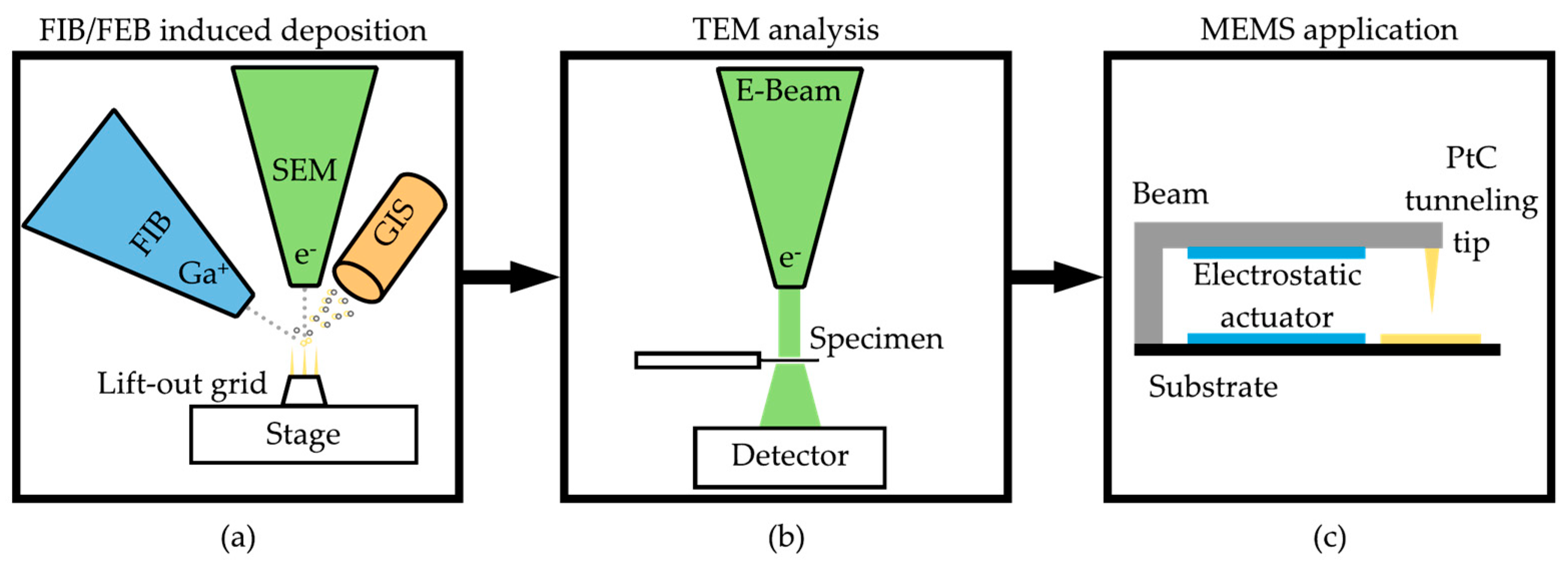
2. Materials and Methods
2.1. Platinum Carbon Composite
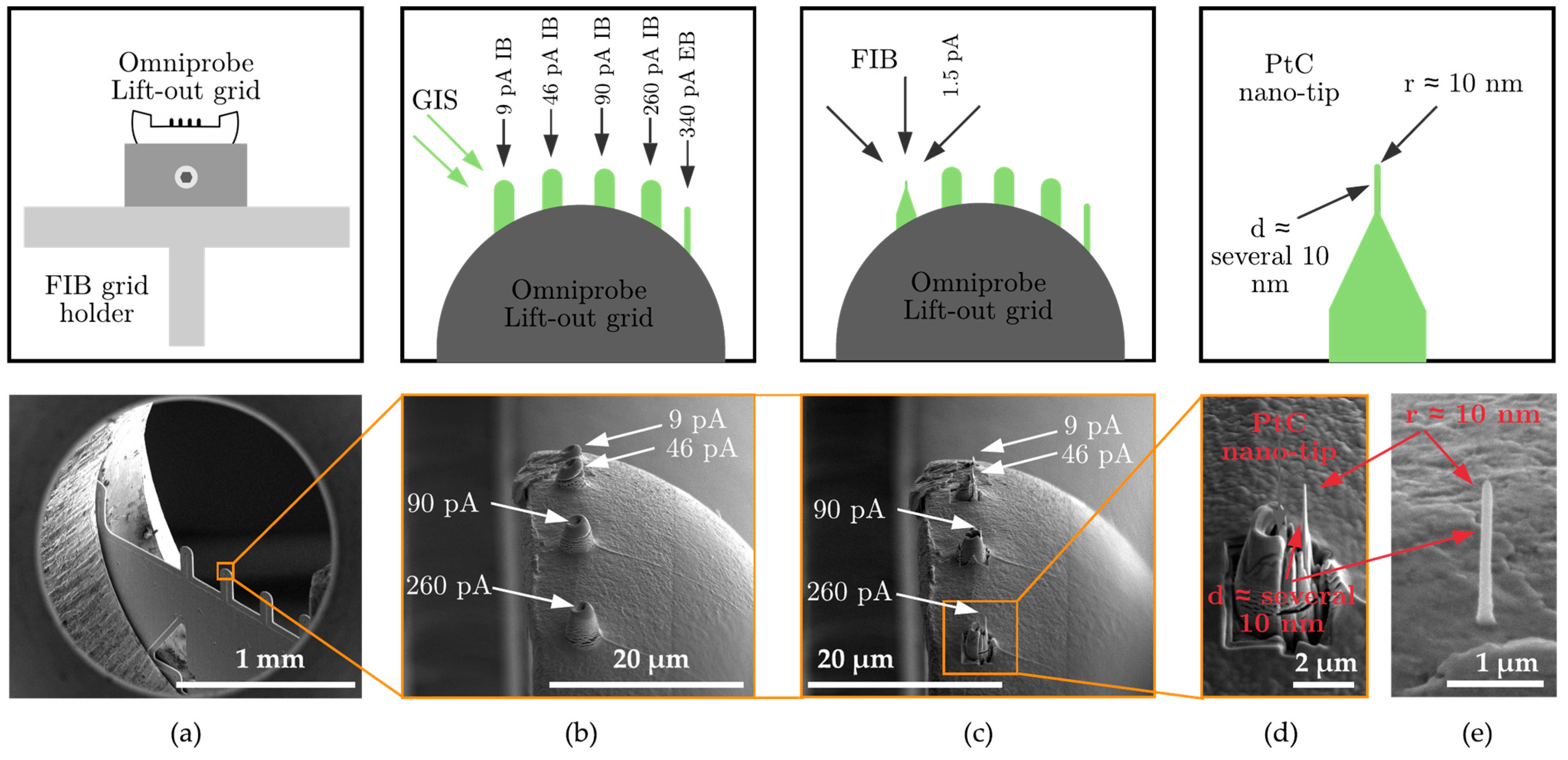
2.2. Specimen Preparation
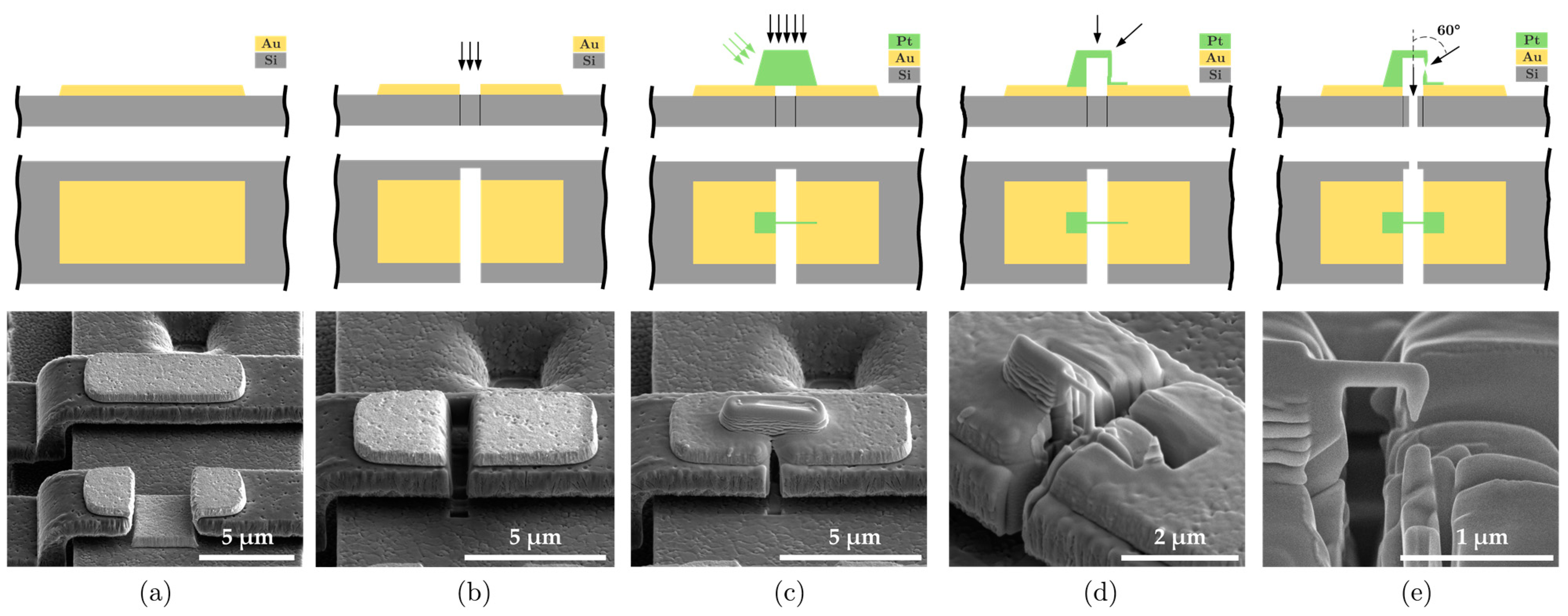
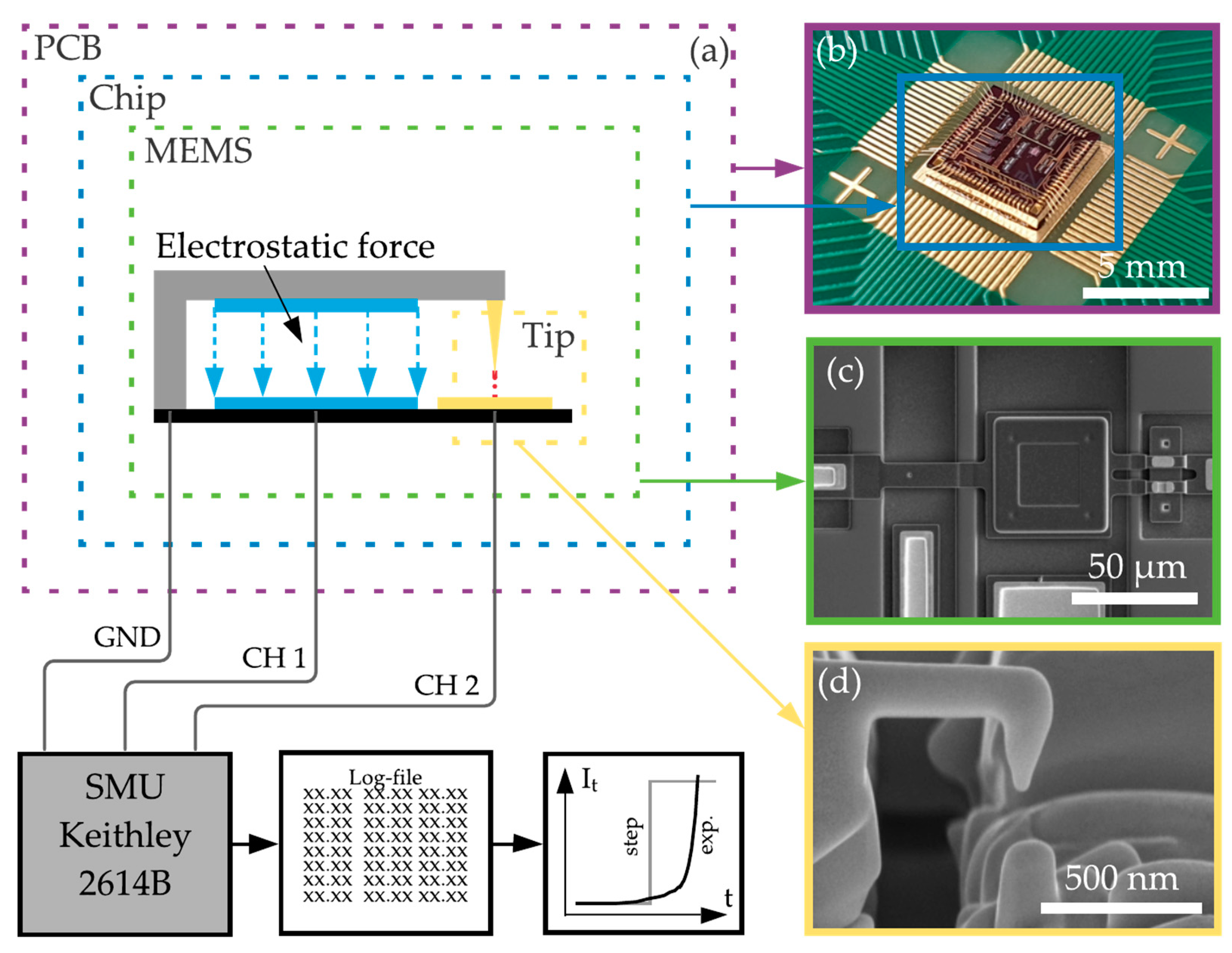
2.3. Tip Integration to MEMS
3. Results
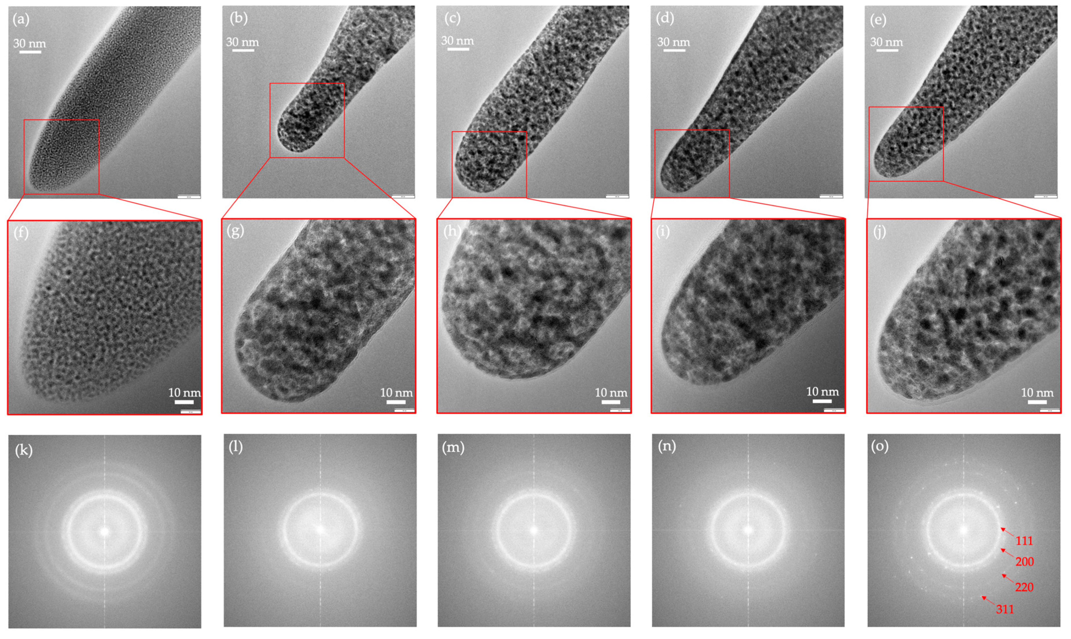
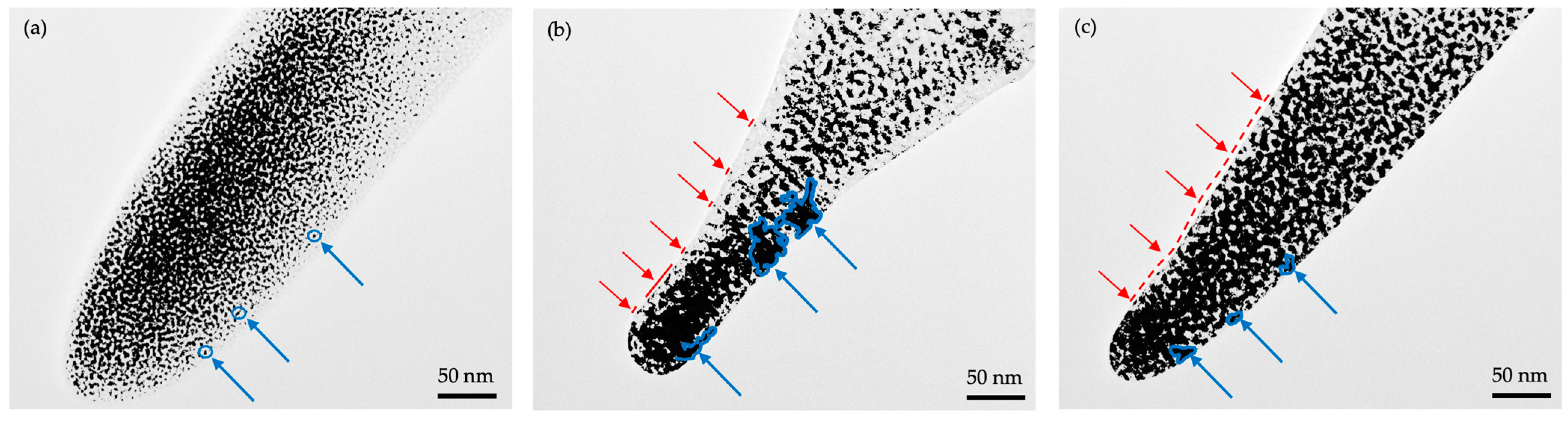
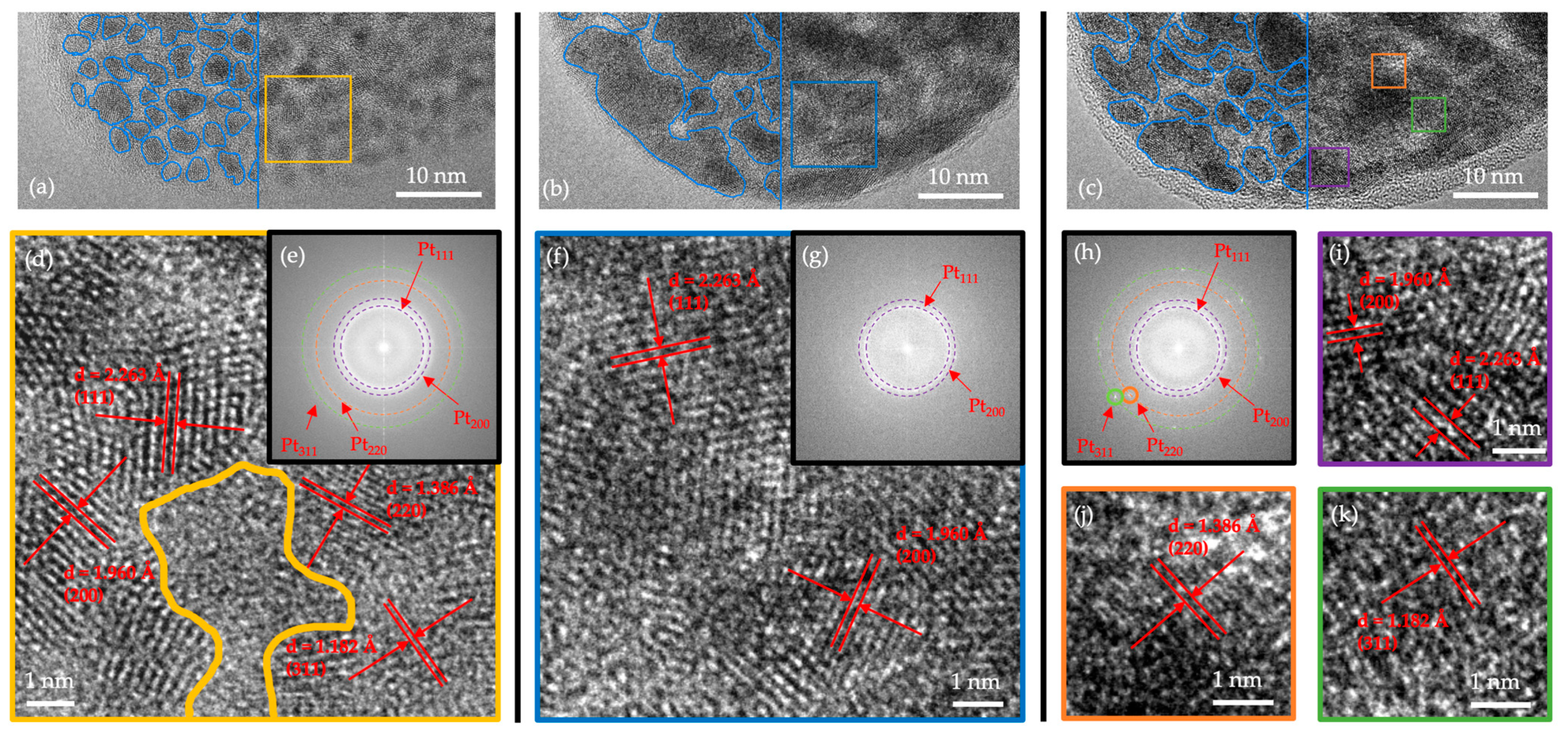
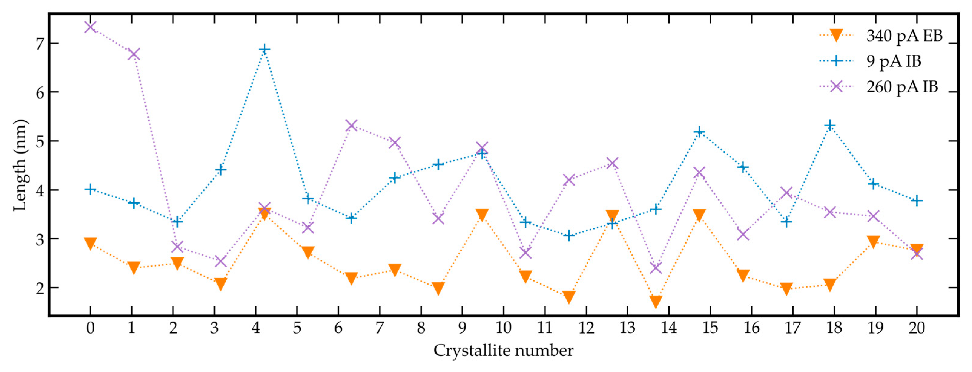
3.1. Transmission Electron Microscopy Analysis
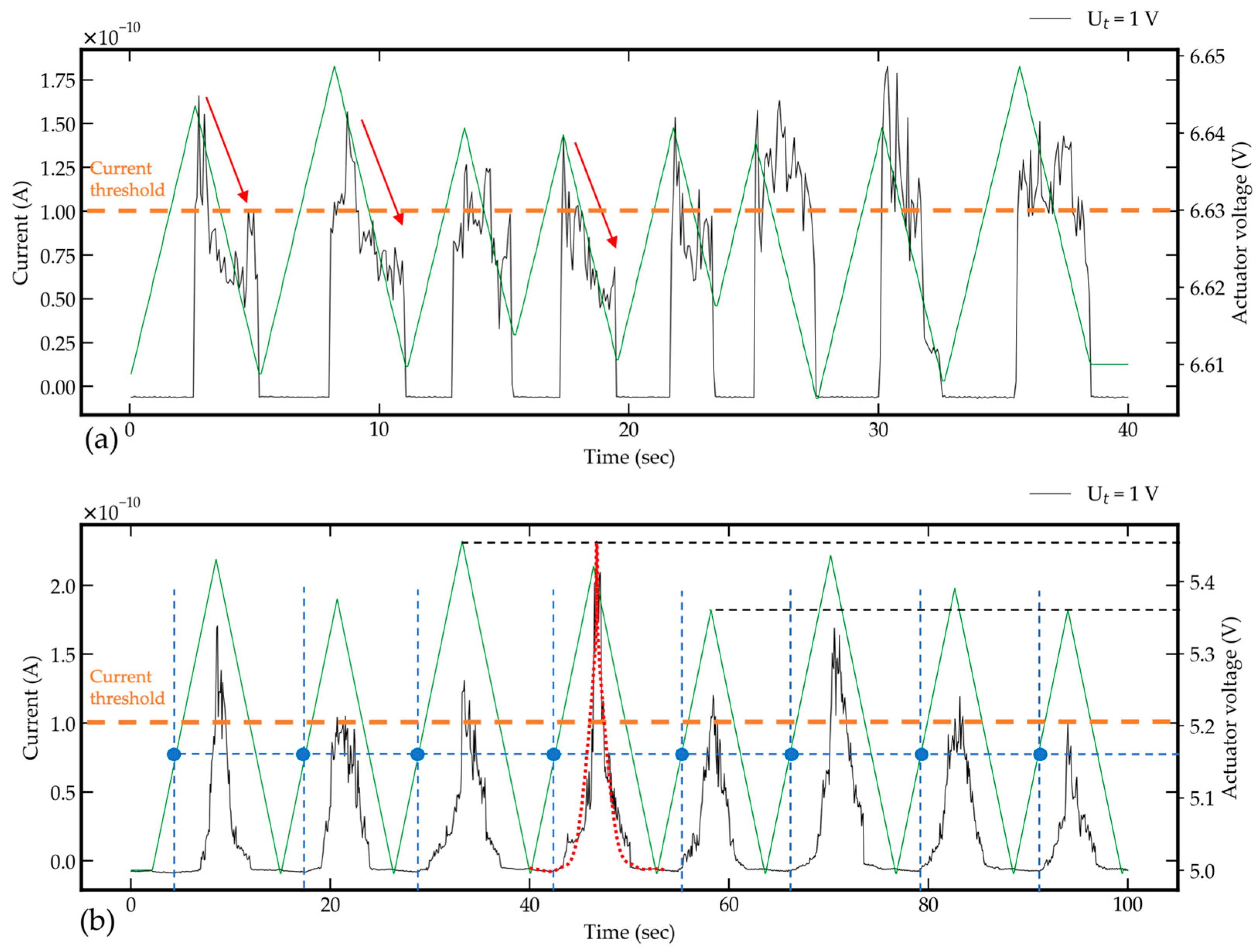
3.2. Tunneling Verification
4. Discussion
5. Conclusions/Summary
Author Contributions
Funding
Institutional Review Board Statement
Informed Consent Statement
Data Availability Statement
Acknowledgments
Conflicts of Interest
References
- Matsui, S.; Kaito, T.; Fujita, J.-I.; Komuro, M.; Kanda, K.; Haruyama, Y. Three-dimensional nanostructure fabrication by focused-ion-beam chemical vapor deposition. J. Vac. Sci. Technol. B Microelectron. Nanometer Struct. 2000, 18, 3181–3184. [Google Scholar] [CrossRef]
- Allameh, S.; Yao, N.; Soboyejo, W. Synthesis of self-assembled nanoscale structures by focused ion-beam induced deposition. Scr. Mater. 2004, 50, 915–919. [Google Scholar] [CrossRef]
- Reyntjens, S.; Puers, R. Focused ion beam induced deposition: Fabrication of three-dimensional microstructures and Young’s modulus of the deposited material. J. Micromech. Microeng. 2000, 10, 181–188. [Google Scholar] [CrossRef]
- Li, W.; Warburton, P.A. Low-current focused-ion-beam induced deposition of three-dimensional tungsten nanoscale conductors. Nanotechnology 2007, 18, 485305. [Google Scholar] [CrossRef]
- Lin, J.-F.; Bird, J.P.; Rotkina, L.; Bennett, P.A. Classical and quantum transport in focused-ion-beam-deposited Pt nanointerconnects. Appl. Phys. Lett. 2003, 82, 802–804. [Google Scholar] [CrossRef]
- Sadki, E.H.; Ooi, S.; Hirata, K. Focused-ion-beam-induced deposition of superconducting nanowires. Appl. Phys. Lett. 2004, 85, 6206–6208. [Google Scholar] [CrossRef] [Green Version]
- De Marzi, G.; Iacopino, D.; Quinn, A.J.; Redmond, G. Probing intrinsic transport properties of single metal nanowires: Direct-write contact formation using a focused ion beam. J. Appl. Phys. 2004, 96, 3458–3462. [Google Scholar] [CrossRef]
- Hernández-Ramírez, F.; Rodríguez, J.; Casals, O.; Russinyol, E.; Vilà, A.; Romano-Rodríguez, A.; Morante, J.; Abid, M. Characterization of metal-oxide nanosensors fabricated with focused ion beam (FIB). Sens. Actuators B Chem. 2006, 118, 198–203. [Google Scholar] [CrossRef]
- Tham, D.; Nam, C.-Y.; Fischer, J.E. Microstructure and Composition of Focused-Ion-Beam-Deposited Pt Contacts to GaN Nanowires. Adv. Mater. 2005, 18, 290–294. [Google Scholar] [CrossRef]
- Vilà, A.; Hernández-Ramírez, F.; Rodriguez, J.; Casals, O.; Romano-Rodriguez, A.; Morante, J.; Abid, M. Fabrication of metallic contacts to nanometre-sized materials using a focused ion beam (FIB). Mater. Sci. Eng. C 2006, 26, 1063–1066. [Google Scholar] [CrossRef]
- Tao, T. Focused ion beam induced deposition of platinum for repair processes. J. Vac. Sci. Technol. B Microelectron. Nanometer Struct. 1991, 9, 162. [Google Scholar] [CrossRef]
- Wägner, A. X-ray mask repair with focused ion beams. J. Vac. Sci. Technol. B Microelectron. Nanometer Struct. 1990, 8, 1557. [Google Scholar] [CrossRef]
- De Marco, A.J.; Melngailis, J. Maskless fabrication of JFETs via focused ion beams. Solid-State Electron. 2004, 48, 1833–1836. [Google Scholar] [CrossRef]
- Gazzadi, G.C.; Frabboni, S. Fabrication of 5 nm gap pillar electrodes by electron-beam Pt deposition. J. Vac. Sci. Technol. B Microelectron. Nanometer Struct. 2005, 23, L1. [Google Scholar] [CrossRef]
- Haub, M.; Bogner, M.; Guenther, T.; Zimmermann, A.; Sandmaier, H. Development and Proof of Concept of a Miniaturized MEMS Quantum Tunneling Accelerometer Based on PtC Tips by Focused Ion Beam 3D Nano-Patterning. Sensors 2021, 21, 3795. [Google Scholar] [CrossRef]
- Penate-Quesada, L.; Mitra, J.; Dawson, P. Non-linear electronic transport in Pt nanowires deposited by focused ion beam. Nanotechnol. 2007, 18, 215203. [Google Scholar] [CrossRef]
- Ballestar, A.; Esquinazi, P. Transport characteristics of focused beam deposited nanostructures. Nanofabrication 2015, 2. [Google Scholar] [CrossRef]
- Fransson, J.; Lin, J.-F.; Rotkina, L.; Bird, J.P.; Bennett, P.A. Signatures of bandlike tunneling in granular nanowires. Phys. Rev. B 2005, 72, 113411. [Google Scholar] [CrossRef] [Green Version]
- Fernández-Pacheco, A.; De Teresa, J.M.; Córdoba, R.; Ibarra, M.R. Metal-insulator transition in Pt-C nanowires grown by focused-ion-beam-induced deposition. Phys. Rev. B 2009, 79, 174204. [Google Scholar] [CrossRef]
- Rotkina, L.; Lin, J.-F.; Bird, J.P. Nonlinear current-voltage characteristics of Pt nanowires and nanowire transistors fabricated by electron-beam deposition. Appl. Phys. Lett. 2003, 83, 4426. [Google Scholar] [CrossRef]
- Labille, J.; Pelinovskaya, N.; Botta, C.; Bottero, J.-Y.; Masion, A.; Joag, D.S.; Forbes, R.G.; Burger, S.; Pomplun, J.; Schmidt, F.; et al. Focused-Ion-Beam Chemical-Vapor-Deposition (FIB-CVD). In Encyclopedia of Nanotechnology; Springer: Dordrecht, The Netherlands, 2012; pp. 866–876. [Google Scholar]
- Kometani, R.; Ichihashi, T.; Kanda, K.; Suzuki, T.; Niihara, K.; Ishihara, S.; Kaito, T.; Matsui, S. Resistivity change of the diamondlike carbon, deposited by focused-ion-beam chemical vapor deposition, induced by the annealing treatment. J. Vac. Sci. Technol. B Microelectron. Nanom. Struct. 2008, 26, 2628–2631. [Google Scholar] [CrossRef]
- De Teresa, J.M.; Córdoba, R.; Fernández-Pacheco, A.; Montero, O.; Štrichovanec, P.; Ibarra, M.R. Origin of the Difference in the Resistivity of As-Grown Focused-Ion- and Focused-Electron-Beam-Induced Pt Nanodeposits. J. Nanomater. 2009, 2009, 936863. [Google Scholar] [CrossRef] [Green Version]
- Koops, H.W.P. Fabrication and characterization of platinum nanocrystalline material grown by electron-beam induced deposition. J. Vac. Sci. Technol. B Microelectron. Nanometer Struct. 1995, 13, 2400. [Google Scholar] [CrossRef]
- Van Dorp, W.F.; Hagen, C.W. A critical literature review of focused electron beam induced deposition. J. Appl. Phys. 2008, 104, 081301. [Google Scholar] [CrossRef] [Green Version]
- Utke, I.; Hoffmann, P.; Melngailis, J. Gas-assisted focused electron beam and ion beam processing and fabrication. J. Vac. Sci. Technol. B Microelectron. Nanom. Struct. 2008, 26, 1197. [Google Scholar] [CrossRef] [Green Version]
- Wiedemair, J.; Menegazzo, N.; Pikarsky, J.; Booksh, K.S.; Mizaikoff, B.; Kranz, C. Novel electrode materials based on ion beam induced deposition of platinum carbon composites. Electrochimica Acta 2010, 55, 5725–5732. [Google Scholar] [CrossRef]
- Langford, R.M.; Wang, T.-X.; Ozkaya, D. Reducing the resistivity of electron and ion beam assisted deposited Pt. Microelectron. Eng. 2007, 84, 784–788. [Google Scholar] [CrossRef]
- Lin, J.-F.; Bird, J.P.; Rotkina, L.; Sergeev, A.; Mitin, V. Large effects due to electron–phonon-impurity interference in the resistivity of Pt/C-Ga composite nanowires. Appl. Phys. Lett. 2004, 84, 3828. [Google Scholar] [CrossRef] [Green Version]
- An, B.-S.; Kwon, Y.; Oh, J.-S.; Shin, Y.-J.; Ju, J.-S.; Yang, C.-W. Evaluation of ion/electron beam induced deposition for electrical connection using a modern focused ion beam system. Appl. Microsc. 2019, 49, 1–5. [Google Scholar] [CrossRef] [Green Version]
- Tao, T. Focused ion beam induced deposition of platinum. J. Vac. Sci. Technol. B Microelectron. Nanometer Struct. 1990, 8, 1826. [Google Scholar] [CrossRef]
- Melngailis, J. Focused Ion Beam Induced Deposition: A Review. In Proceedings of the Proc. SPIE 1465, Electron-Beam, X-Ray, and Ion-Beam Submicrometer Lithographies for Manufacturing; Peckerar, M.C., Ed.; SPIE: San Jose, CA, USA, 1 August 1991; p. 36. [Google Scholar]
- Schwalb, C.H.; Grimm, C.; Baranowski, M.; Sachser, R.; Porrati, F.; Reith, H.; Das, P.; Müller, J.; Völklein, F.; Kaya, A.; et al. A Tunable Strain Sensor Using Nanogranular Metals. Sensors 2010, 10, 9847–9856. [Google Scholar] [CrossRef] [PubMed]
- Gates-Rector, S.; Blanton, T. The Powder Diffraction File: A quality materials characterization database. Powder Diffr. 2019, 34, 352–360. [Google Scholar] [CrossRef] [Green Version]

| Plane | d [Å] |
|---|---|
| 111 | 2.2650 |
| 200 | 1.9616 |
| 220 | 1.3873 |
| 311 | 1.1826 |
Publisher’s Note: MDPI stays neutral with regard to jurisdictional claims in published maps and institutional affiliations. |
© 2021 by the authors. Licensee MDPI, Basel, Switzerland. This article is an open access article distributed under the terms and conditions of the Creative Commons Attribution (CC BY) license (https://creativecommons.org/licenses/by/4.0/).
Share and Cite
Haub, M.; Günther, T.; Bogner, M.; Zimmermann, A. Investigation of Focused Ion and Electron Beam Platinum Carbon Nano-Tips with Transmission Electron Microscopy for Quantum Tunneling Vacuum Gap Applications. Appl. Sci. 2021, 11, 11793. https://doi.org/10.3390/app112411793
Haub M, Günther T, Bogner M, Zimmermann A. Investigation of Focused Ion and Electron Beam Platinum Carbon Nano-Tips with Transmission Electron Microscopy for Quantum Tunneling Vacuum Gap Applications. Applied Sciences. 2021; 11(24):11793. https://doi.org/10.3390/app112411793
Chicago/Turabian StyleHaub, Michael, Thomas Günther, Martin Bogner, and André Zimmermann. 2021. "Investigation of Focused Ion and Electron Beam Platinum Carbon Nano-Tips with Transmission Electron Microscopy for Quantum Tunneling Vacuum Gap Applications" Applied Sciences 11, no. 24: 11793. https://doi.org/10.3390/app112411793
APA StyleHaub, M., Günther, T., Bogner, M., & Zimmermann, A. (2021). Investigation of Focused Ion and Electron Beam Platinum Carbon Nano-Tips with Transmission Electron Microscopy for Quantum Tunneling Vacuum Gap Applications. Applied Sciences, 11(24), 11793. https://doi.org/10.3390/app112411793