Article

Structural Analysis, Phase Stability, Electronic Band Structures, and Electric Transport Types of (Bi2)m(Bi2Te3)n by Density Functional Theory Calculations

Energy Conversion Research Center, Korea Electrotechnology Research Institute (KERI), Changwon 51543, Korea
*
Author to whom correspondence should be addressed.
Appl. Sci. 2021, 11(23), 11341; https://doi.org/10.3390/app112311341
Submission received: 9 October 2021 / Revised: 22 November 2021 / Accepted: 24 November 2021 / Published: 30 November 2021
(This article belongs to the Special Issue Automobile Energy Harvesting Technologies)

Abstract

:
Thermoelectric power generation is a promising candidate for automobile energy harvesting technologies because it is eco-friendly and durable owing to direct power conversion from automobile waste heat. Because Bi−Te systems are well-known thermoelectric materials, research on (Bi2)m(Bi2Te3)n homologous series can aid the development of efficient thermoelectric materials. However, to the best of our knowledge, (Bi2)m(Bi2Te3)n has been studied through experimental synthesis and measurements only. Therefore, we performed density functional theory calculations of nine members of (Bi2)m(Bi2Te3)n to investigate their structure, phase stability, and electronic band structures. From our calculations, although the total energies of all nine phases are slightly higher than their convex hulls, they can be metastable owing to their very small energy differences. The electric transport types of (Bi2)m(Bi2Te3)n do not change regardless of the exchange–correlation functionals, which cause tiny changes in the atomic structures, phase stabilities, and band structures. Additionally, only two phases (Bi8Te9, BiTe) became semimetallic or semiconducting depending on whether spin–orbit interactions were included in our calculations, and the electric transport types of the other phases were unchanged. As a result, it is expected that Bi2Te3, Bi8Te9, and BiTe are candidates for thermoelectric materials for automobile energy harvesting technologies because they are semiconducting.

1. Introduction

Gasoline and hybrid electric vehicles cause waste heat energy to be released into the environment because of inefficient conversion of approximately 25% from chemical energy into mechanical energy through exhaust gases and coolants [1,2,3]. Automobile energy harvesting technology has attracted significant attention from the automobile industry to reduce the fuel consumption of vehicles [3,4]. In addition, automobile waste heat recovery has been intensively investigated to alleviate global warming and improve the efficiency of vehicles [1,2,4,5,6,7,8,9]. Meanwhile, thermoelectric generators are eco-friendly and durable owing to direct power conversion into electricity from automobile waste heat [1,2,4,5,6,8,9]. As a result, energy harvesting using thermoelectric generators in automobiles has been considered as an option to recover automobile waste heat.
The Seebeck effect and conversion efficiency are important in thermoelectric energy harvesting technology. The thermoelectric dimensionless figure of merit (ZT) is defined as ZT = α2σT/κ, where α is the Seebeck coefficient, σ is the electrical conductivity, κ is the thermal conductivity, and T is the absolute temperature [9,10]. The thermoelectric conversion efficiency (η) is defined as η = Pout/Qh, where Pout is the electric output power and Qh is the heat input [9,10]. Many researchers have investigated thermoelectric materials with high ZT and η for applications in thermoelectric energy harvesting [6,11,12,13].
Meanwhile, (Bi2)m(Bi2Te3)n homologous series have been investigated as layer-stacked structures consisting of Bi bilayers and Bi2Te3 quintuple layers. In addition, they have been synthesised experimentally and their structural (lattice parameters, volume, etc.) and thermoelectric properties (resistivity, Seebeck coefficient, etc.) have been measured [14,15,16,17,18]. In particular, it has been demonstrated that (Bi2)m(Bi2Te3)n exhibits intrinsically low lattice thermal conductivity due to chemical bond softening and lattice anharmonicity [18]. However, to the best of our knowledge, no research has been conducted on the structural analysis and electronic band structures of (Bi2)m(Bi2Te3)n.
First-principles density functional theory calculations of the (Bi2)m(Bi2Te3)n homologous series were performed to investigate their internal structures, phase stability from mixing energies, and electronic band structures. From the structural analysis, it was found that exchange–correlation functionals affect both the intralayer thickness and interlayer distances of (Bi2)m(Bi2Te3)n. Further, it was revealed that the (Bi2)m(Bi2Te3)n homologous series can be metastable from a comparison between their layer mixing energies and the convex hull. In addition, the energy gaps and band edges of (Bi2)m(Bi2Te3)n were determined from electronic band structure calculations. Consequently, electric transport types were obtained, and the (Bi2)m(Bi2Te3)n considered here were semimetallic or semiconducting. In particular, Bi2Te3, Bi8Te9, and BiTe among the (Bi2)m(Bi2Te3)n homologous series were semiconducting. Therefore, Bi2Te3, Bi8Te9, and BiTe are expected to be feasible thermoelectric materials for applications in automobile energy harvesting.

2. Methods and Calculations Details

First-principles density functional theory (DFT) [19,20] calculations were performed. The DFT calculations were implemented using the Vienna Ab initio simulation package [21,22,23]. A plane-wave basis set with an energy cut-off of 300 eV was used with the Perdew–Burke–Ernzerhof (PBE) exchange correlational functional (Exc) [24], and local density approximation (LDA) [23] and projector augmented wave (PAW) pseudopotentials [25,26] were used: PAW_PBE Bi_d_GW 14Apr2014, PAW_PBE Te_GW 22Mar2012 for PBE and PAW Bi_d_GW 14Apr2014, PAW Te_GW 22Mar2012 for LDA. A 12 × 12 × k 3   Γ -centered k-point mesh grid was used to sample the k-point in the Brillouin zone, where k 3 is a subdivision of the third direction along the third reciprocal lattice vector. To consider the relativistic correction of heavy elements such as Bi and Te, the spin–orbit interaction (SOI) was employed [27,28,29].
The structures of the (Bi2)m(Bi2Te3)n homologous series considered here were obtained from Bos’ research [14]. Their end members were semiconducting Bi2Te3 and semimetallic Bi2; nine members of the series were studied: Bi2Te3, Bi4Te5, Bi6Te7, Bi8Te9, BiTe, Bi4Te3, Bi2Te, Bi7Te3, and Bi2. Here, the ratio of Bi2 to Bi2Te3 increased in the following order from Bi2Te3 to Bi2 as the ratio of m to n: 0:3, 1:5, 2:7, 3:9, 1:2, 3:3, 2:1, 15:6, and 3:0 (see Figure 1). In the figure, the side view shows the atomic structure viewed from the a-axis direction, and the top view shows the atomic structure viewed from the c-axis direction. The purple spheres represent Bi atoms and the gold spheres are Te atoms. The red blocks are the Bi bilayers (BLs) and the blue blocks the Bi2Te3 quintuple layers (QLs). The lattice parameters of the a-axis and the c-axis in the hexagonal supercells were obtained from previous experimental studies of (Bi2)m(Bi2Te3)n materials [14,15,16,17] (see Table 1). In particular, we referred to the layer-stacking method of BL and QL in Bos’ study [14]; for convenient calculations, the different stacking methods of BL and QL were not considered. Furthermore, the optimised atomic structure of each material of (Bi2)m(Bi2Te3)n was obtained while lowering the total force acting on each atom below 10−3 eV/Å, where the initial atomic structure had fixed lattice parameters with all the atoms arrayed equidistantly in the direction of the c-axis.
In the atomic structure of the (Bi2)m(Bi2Te3)n homologous series, the number of BLs or QLs was defined as NBL or NQL, respectively. The total number of atoms in each phase was defined as NAtom. Furthermore, the average thickness of BL or QL was defined as the intralayer thickness of BL or QL. Additionally, the average distance between BL and BL, BL and QL, or QL and QL was defined as the interlayer distances of BL−BL, BL−QL, or QL−QL, respectively (see Table 1 and Figure 1).
To investigate the relative stability of (Bi2)m(Bi2Te3)n when mixing BL and QL, the layer mixing energy of each phase per atom was defined as
E Mixing = E Total ( Bi 2 ) m ( Bi 2 Te 3 ) n   m   E Total Bi 2   n   E Total Bi 2 Te 3 N atom
where E Total ( Bi 2 ) m ( Bi 2 Te 3 ) n , E Total Bi 2 , and E Total Bi 2 Te 3 are the total energies of ( Bi 2 ) m ( Bi 2 Te 3 ) n , Bi 2 , and Bi 2 Te 3 , respectively. Note that EMixing is normalised by the total atomic number in the supercell (Natom) to reflect only the structural differences between the (Bi2)m(Bi2Te3)n phases. In addition, note that only zero-temperature EMixing is displayed here because the temperature dependence of EMixing is not of interest.
Our electronic band structures with density of states (DOS) were generated using pymatgen [30] based on our DFT calculations. In our band calculations, the electronic band structures of the full k-point path (Γ−M−K−Γ−A−L−H−A, L−M, K−H) were obtained with 51 mesh grids in the first Brillouin zone of hexagonal lattices. From this, it was found that all the valence band maximum (VBM) and conduction band minimum (CBM) of the (Bi2)m(Bi2Te3)n considered in this study were located in the k-point path of K−Γ−M or L−A−H for our calculation setting: K (0.333, 0.333, 0), Γ (0, 0, 0), M (0.5, 0, 0), L (0.5, 0, 0.5), A (0, 0, 0.5), H (0.333, 0.333, 0.5). Consequently, only electronic band structures in K−Γ−M and L−A−H are presented for the Exc used in our calculations. In addition, our electronic band structures were projected onto atomic elements (Bi: blue, Te: red), except for Bi2, and our DOS is projected onto electronic orbitals (s: blue, p: red, d: green, f: violet). For the electronic band topology of (Bi2)m(Bi2Te3)n phases, the direct bandgap was defined as E gap d (the minimum of the difference between CBM and VBM at the same k-point) and the indirect bandgap as E gap i (the difference between CBM and VBM). Electric types were defined to determine the electric transport characteristics of (Bi2)m(Bi2Te3)n: semiconductors if both E gap d and E gap i were positive, semimetals if E gap d was positive and E gap i negative, and metals if both E gap d and E gap i were negative.

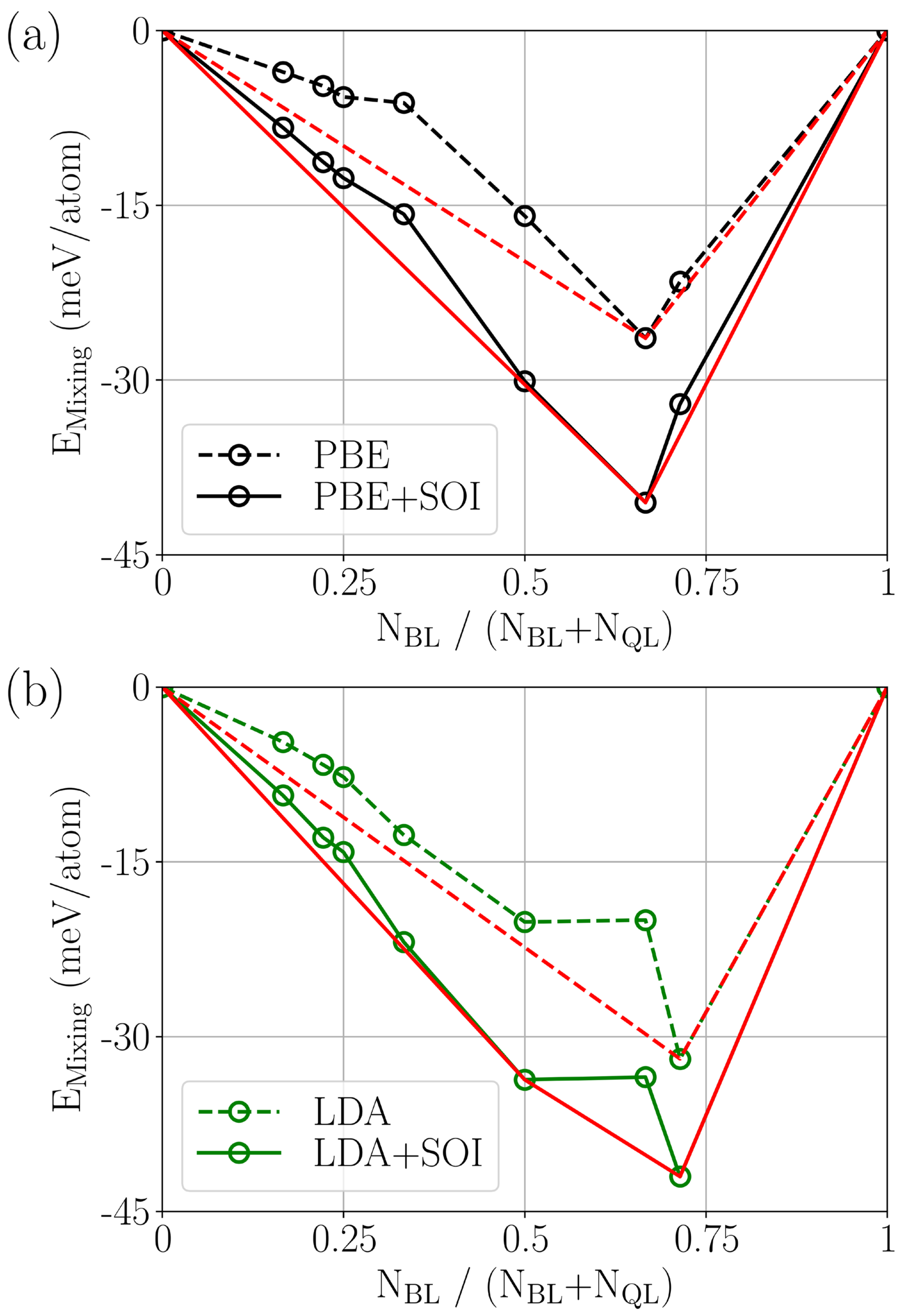
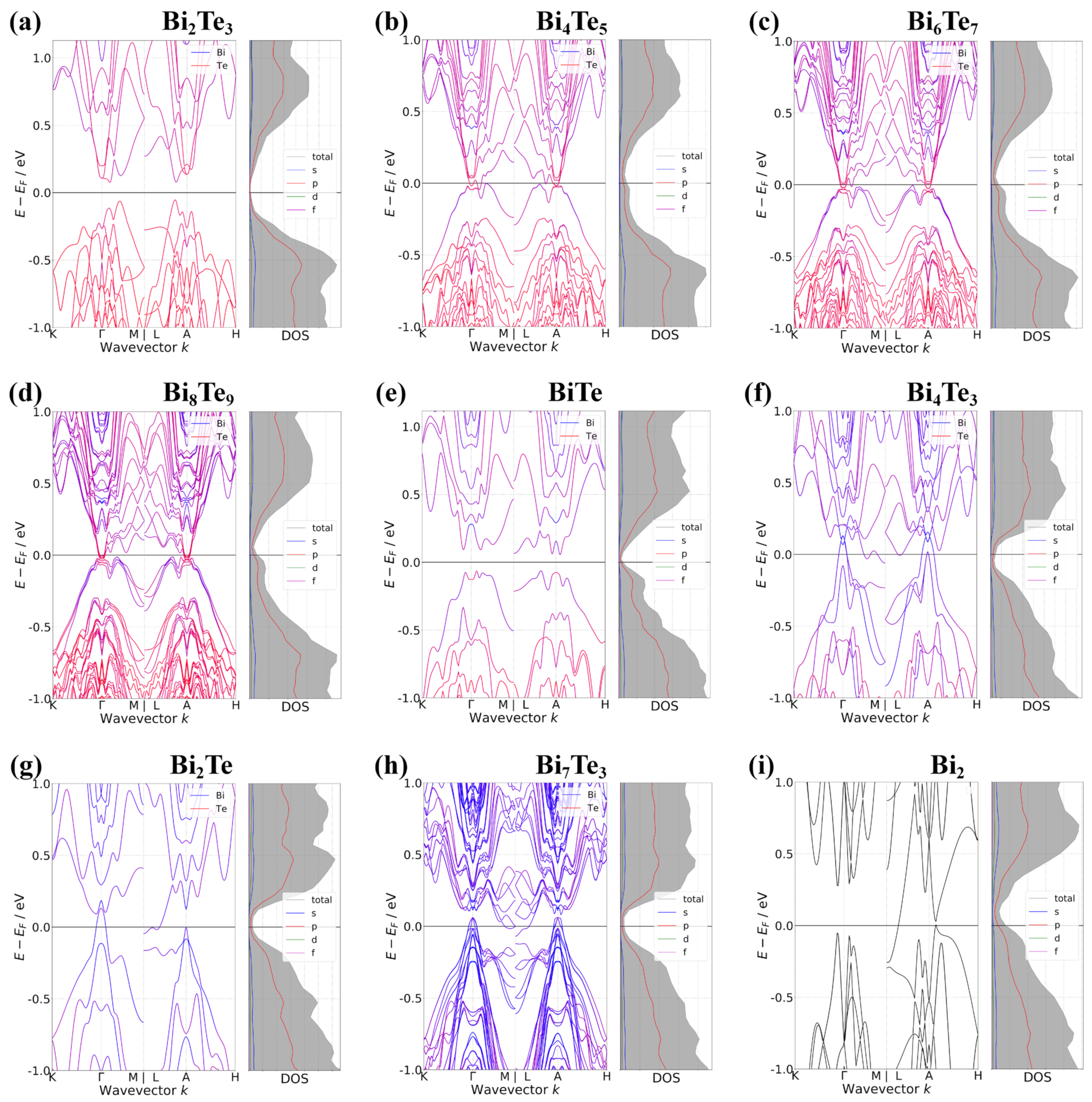
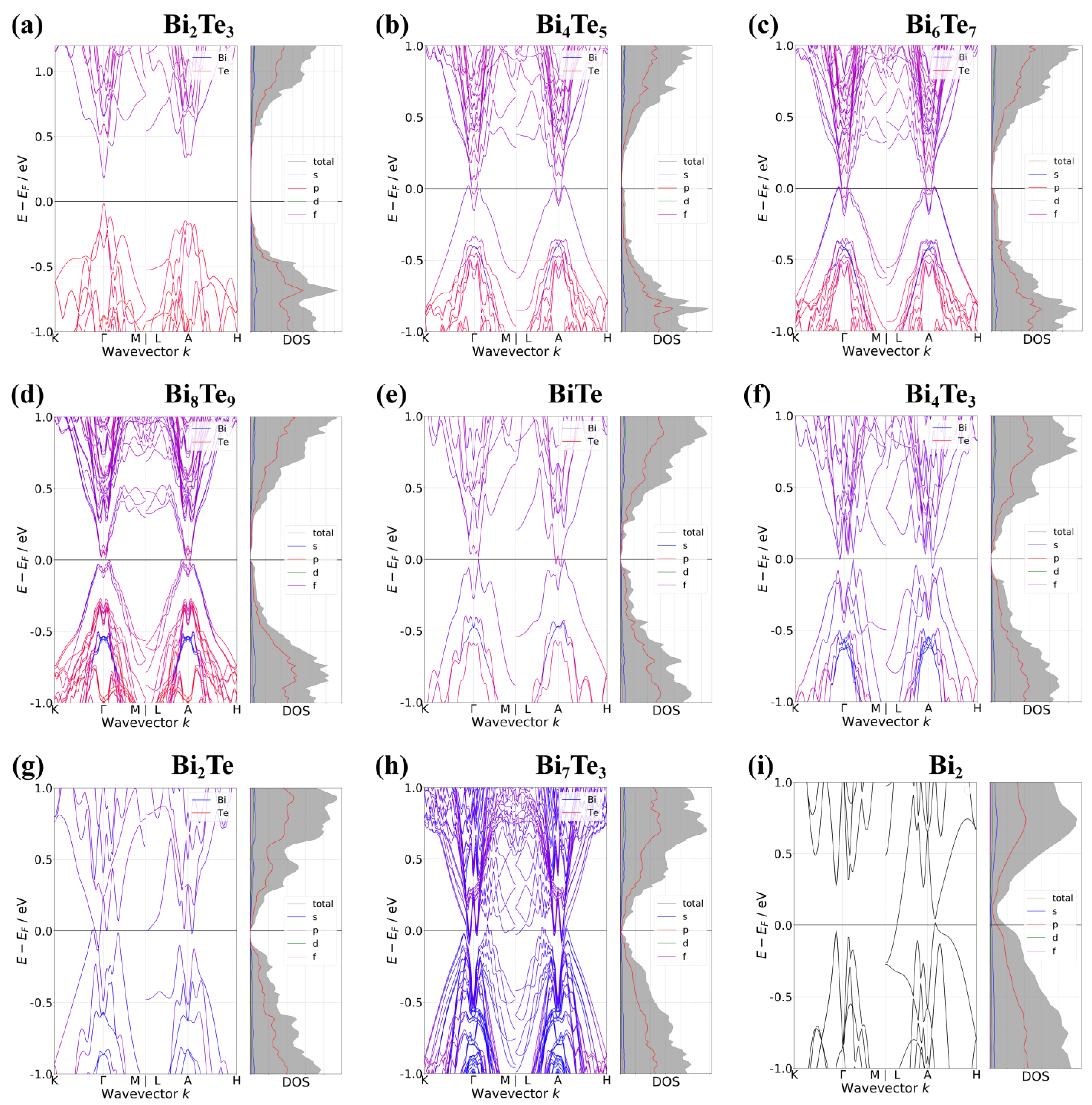
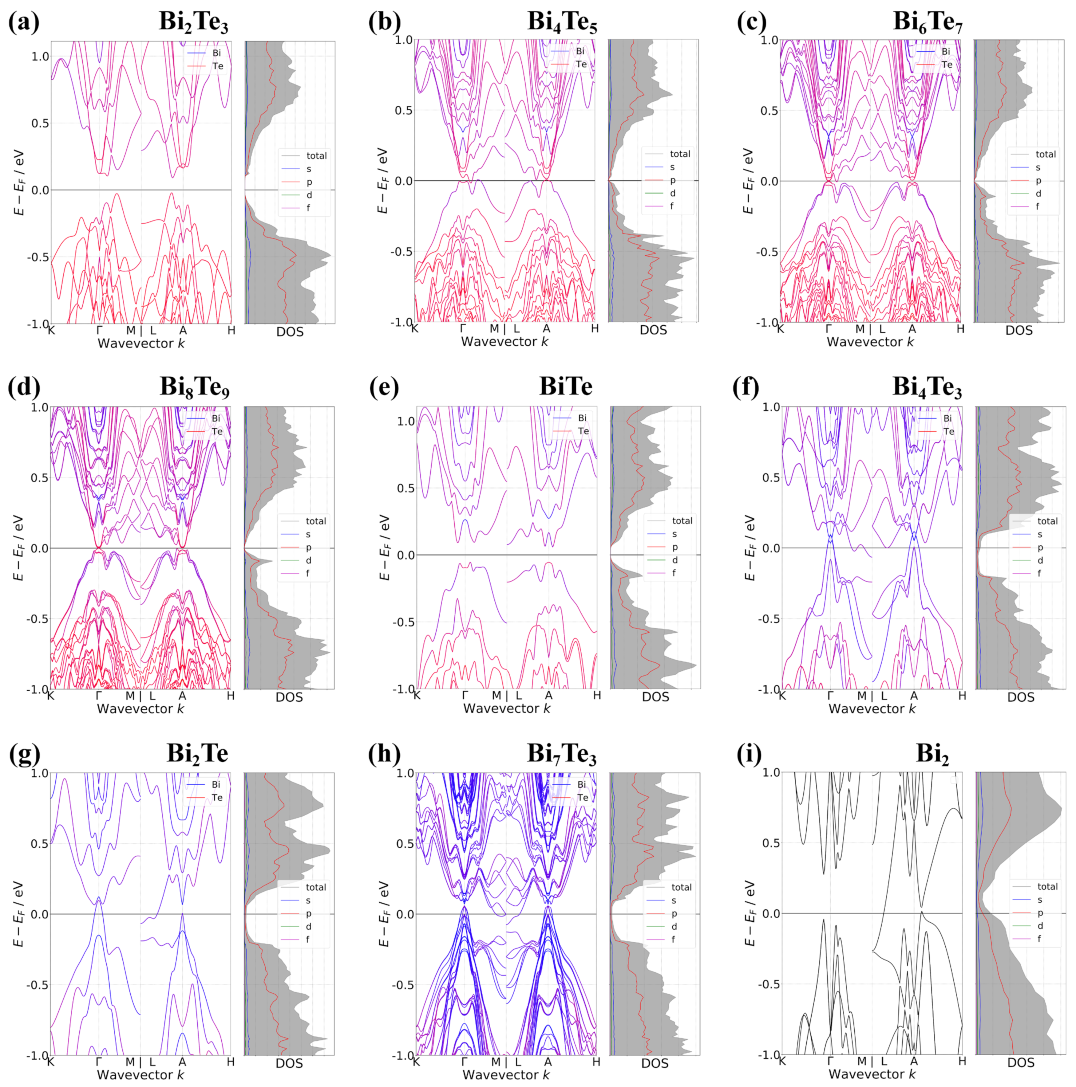
3. Results and Discussions

Table 1 shows the chemical formula, hexagonal composition, ratio between the number of BLs and QL (NBL:NQL), ratio between NBL and the total number of layers (NBL/(NBL + NQL)), lattice volume per atom (Volume/NAtom), lattice constants in a hexagonal supercell (aHex, cHex), cHex per atom (cHex/NAtom), average intralayer thickness, and average interlayer distance depending on Exc with (w/) or without (w/o) SOI used in our calculations. Note that NAtom is the same as the total number of layers in each phase because our unit cells contain only a single atom on one layer. Additionally, note that NBL/NAtom increases from 0 to 1 as the proportion of BL increases from Bi2Te3 to Bi2. In addition, for each (Bi2)m(Bi2Te3)n, the lattice parameters in the a vector direction were 4.388–4.546 Å, the lattice parameters in the c vector direction were 11.862–119 Å, and the volume per atom (Volume/NAtom) was 33.887–35.383 Å3. The average lattice parameters along the c-axis with respect to the number of layers were 1.977–2.033 Å.
The intralayer thicknesses of the atomic structure of (Bi2)m(Bi2Te3)n obtained through the DFT calculations were investigated, except for Bi2 and Bi2Te3. Based on the intralayer thickness without considering the SOI, the rate of increase of each intralayer thickness was calculated depending on whether or not SOI was considered. Regardless of the type of Exc used, the intralayer thickness with respect to SOI increased significantly compared to the thickness without considering SOI. In the case of PBE, the intralayer thicknesses of BL and QL for (Bi2)m(Bi2Te3)n were 1.697 Å and 7.472 Å for Bi4Te5, 1.693 Å and 7.453 Å for Bi6Te7, 1.701 Å and 7.492 Å for Bi8Te9, 1.692 Å and 7.449 Å for BiTe, 1.681 Å and 7.415 Å for Bi4Te3, 1.671 Å and 7.390 Å for Bi2Te, and 1.674 Å and 7.358 Å, Bi7Te3, respectively. In PBE with SOI, compared to PBE, the thickness of BL increases by 1.64–3.63% and the thickness of QL also increases by 0.69–1.25% depending on their atomic structures. In LDA, the intralayer thicknesses of BL and QL for (Bi2)m(Bi2Te3)n were 1.661 Å and 7.403 Å for Bi4Te3, 1.657 Å and 7.384 Å for Bi6Te7, 1.664 Å and 7.419 Å for Bi8Te9, 1.657 Å and 7.383 Å for BiTe, 1.645 Å and 7.346 Å for Bi4Te3, 1.632 Å and 7.310 Å for Bi2Te, and 1.638 Å and 7.291 Å for Bi7Te3, respectively. In LDA with SOI, compared to LDA, the thickness of BL increases by 1.40–3.51% and that of QL by 0.75–1.49%. Consequently, all increase rates of the intralayer thickness have positive values regardless of the intralayer type and the thickness of BL increases by more than 1.8 times of QL if SOI is considered, regardless of the phase of (Bi2)m(Bi2Te3)n. In addition, considering the SOI, the intralayer thickness of BL for PBE increases more than that of BL for LDA, although that of QL for PBE increases less than that of QL for LDA. This indicates that the Exc of PBE (PBE w/o or w/SOI) overestimates the intralayer thickness of BL by more than 2% compared to that of LDA (LDA w/o or w/SOI). Furthermore, this indicates that the intralayer thickness of QL is overestimated by less than 1.1% by PBE compared with LDA. Thus, this shows that LDA underestimates the distances between adjacent atoms along the c-axis in the intralayers compared with PBE.
The interlayer distances of (Bi2)m(Bi2Te3)n were also analysed. Depending on the layer stacking in (Bi2)m(Bi2Te3)n, there were BL–BL, BL–QL, and QL–QL interlayer distances; BL–BL interfaces were only observed in Bi2Te and Bi7Te3; BL–QL interfaces were present in the remaining phases except for Bi2Te3 and Bi2; and QL–QL interfaces were observed in Bi2Te3, Bi4Te3, Bi6Te7, Bi8Te9, and BiTe. PBE (LDA) calculation gives the interlayer distances, as shown in Table 1. For BL–BL in PBE, the interlayer distances are almost unaffected by considering SOI owing to their increase of less than 1%. However, for BL–QL, when considering SOI, their interlayer distances decrease by more than 1.3% when NBL/NLayer ≥ 0.333, although they remain almost constant for the other phases owing to their changes of less than 1.3%. For QL–QL, owing to SOI, their interlayer distances were reduced by more than 3.5%, unlike BL–BL and BL–QL; in particular, LDA decreased the interlayer distances of QL–QL by more than 1% compared to PBE, except for Bi2Te3. Thus, employing SOI in our calculations caused greater changes in the interlayer distances of QL–QL than those of the other interfaces. This revealed that PBE underestimated the interlayer distances compared to LDA: over 2% for BL–BL, over 1.5% for BL–QL, and over 1.5% for QL–QL.
Figure 2 shows the layer mixing energies (EMixing) of (Bi2)m(Bi2Te3)n as a function of NBL/NLayer = NBL/(NBL + NQL). Because there is no layer mixing between QL and BL in Bi2Te3 and Bi2, their EMixing is zero. Figure 2a shows the convex hull and EMxing in PBE and PBE + SOI. In PBE + SOI, EMxing exhibits a convex hull through Bi2Te3–Bi2Te–Bi2. Compared to the convex hull, the EMixing differs by 0.0017 eV/atom for Bi4Te5, 0.0022 eV/atom for Bi6Te7, 0.0025 eV/atom for Bi8Te9, 0.0045 eV/atom for BiTe, 0.0003 eV/atom for Bi4Te3, and 0.0027 eV/atom for Bi7Te3, respectively. The EMixing of PBE is similar to that of PBE + SOI with a few exceptions: in PBE, the difference between the convex hull and EMxing was, on average, ~1.7 times larger than that in PBE + SOI, except for Bi4Te3 and Bi7Te3, whereas in PBE, the differences of Bi4Te3 and Bi7Te3 were ~13.6 and ~0.4 times larger than those in PBE + SOI, respectively. In fact, the differences are less than 0.0045 eV/atom, except for that of BiTe in PBE (0.0070 eV/atom). This indicates that the (Bi2)m(Bi2Te3)n phases can exist energetically because their EMixing is very close to their convex hulls. Meanwhile, considering the SOI, overall EMixing, on average, decreased by 0.0095 eV; the maximum decrease was 0.014 eV for Bi4Te3, and the minimum was 0.0048 eV for Bi4Te5. This indicates that EMixing was overestimated by the PBE calculations with SOI than those without SOI. On the other hand, Figure 2b exhibits a convex hull and EMixing in LDA and LDA + SOI. Note that the convex hulls of LDA functionals (LDA and LDA + SOI) have different shapes from those of PBE functionals (PBE and PBE + SOI). In particular, the convex hull of LDA passes through Bi2Te3–Bi7Te3–Bi2 and that of LDA + SOI through Bi2Te3–Bi4Te3–Bi7Te3–Bi2. Compared to the convex hull in LDA + SOI, EMixing differs by 0.0019 eV for Bi4Te5, 0.0021 eV for Bi6Te7, 0.0027 eV for Bi8Te9, 0.0006 eV for BiTe, and 0.0067 eV for Bi2Te. In LDA, the difference between the convex hull and EMxing was, on average, about two times larger than that in LDA + SOI except for Bi8Te9 and Bi4Te3; in particular, that of BiTe was ~3.8 times larger. The differences were less than 0.0035 eV, except for those of Bi2Te in LDA (0.0098 eV) and LDA + SOI (0.0067 eV). In addition, considering the SOI, overall EMixing, on average, decreased by 0.0091 eV; the maximum decrease was 0.0135 eV for Bi4Te3, and the minimum was 0.0046 eV for Bi4Te5. Thus, this demonstrates that LDA overestimates the phase stabilities of (Bi2)m(Bi2Te3)n compared to PBE.
Figure 3, Figure 4, Figure 5 and Figure 6 show the electronic band structures with their DOS for (Bi2)m(Bi2Te3)n obtained using PBE or LDA calculations, without and with SOI, respectively. All the DOS comprised small components of s- and d-orbital as well as that of large p-orbital in the whole energy range of electrons. It is clear that the orbitals of Bi 6p and Te 5p mainly contribute to the dominant p-orbital component. Note that the shapes of the electronic band structures are more complicated than the NAtom increases due to supercell calculations. Meanwhile, for the convenience of band structure analysis, the VBM and CBM of each phase were used and the band topology near the band edge (VBM, CBM) was investigated. The E gap d and E gap i of all the phases and their reciprocal positions were obtained. From this, the electrical transport types (semiconductor, semimetal, or metal) of all the phases were investigated. The electric transport types with the band structures using PBE and LDA are summarised in Table 2 and Table 3, respectively.
PBE calculations give the electronic band structures shown in Figure 3. The band structure of Bi2Te3 is shown in Figure 3a. There is a VBM of −0.136 eV at Γ and a CBM of 0.136 at Γ, indicating that Bi2Te3 is a semiconductor as previously reported [31,32,33]. Note that the experimental energy gap is about 0.13 eV. Figure 3d shows that Bi8Te9 has a VBM of −0.004 eV on A−H (0.033, 0.033, 0.5), CBM of −0.03 eV on A−H (0.007, 0.007, 0.5), and E gap d of 0.027 eV on A−L (0.02, 0, 0.5). The band structure of BiTe in Figure 3e shows that VBM is 0.017 eV on Γ−M (0.06, 0, 0), CBM is −0.023 eV on A−H (0.013, 0.013, 0.5), and E gap d is 0.035 eV on Γ−M (0.06, 0, 0). The band structure of Bi2 is shown in Figure 3i, where VBM is 0.066 eV on A−H (0.047, 0.047, 0.5), CBM is −0.197 eV on A−L (0.48, 0, 0.5), and E gap d is 0.02 eV on A−H (0.047, 0.047, 0.5). Note that our result for Bi2 is consistent with the experimental reports that bulk Bi is semimetallic [34] since the supercell of Bi2 is to be bulk Bi. Additionally, the other phases (Bi4Te5, Bi6Te7, Bi4Te3, Bi2Te, Bi7Te3) were semimetallic, as shown in Figure 3 and Table 2. Note that PBE showed that the electric transport types of (Bi2)m(Bi2Te3)n were semimetallic because of positive E gap d and negative E gap i except for Bi2Te3. In addition, the electric transport types of (Bi2)m(Bi2Te3)n from LDA are the same as those from PBE, although the detailed values (EVBM, kVBM, ECBM, kCBM, E gap i , k gap i ) of LDA were different from those of PBE (see Figure 3, Figure 4 and Figure 5 and Table 2 and Table 3).
Meanwhile, when considering the SOI in the PBE calculations, there are some changes in the band structures (see Figure 4 and Table 2). In our results, SOI flattens the electronic band of (Bi2)m(Bi2Te3)n in the vicinity of the band edges (VBM and CBM) because dE/dk decreases near these edges. We expect that this is related to the change in the electronic effective mass near the VBM and CBM, although it was not quantitatively analysed. For Bi2Te3, the SOI calculations accompanied an increase in the energy level of VBM (−0.061 eV) and a decrease in that of CBM (0.068 eV), resulting in a slight decrease in energy gaps ( E gap i = 0.129 eV, E gap d = 0.135 eV). For Bi2, the SOI calculation increases both VBM (0.113 eV) and CBM (-0.048 eV), leading to a small increase in the energy gap values ( E gap i = −0.161 eV, E gap d = 0.079 eV). In addition, for BiTe, the SOI calculations decrease VBM (−0.064 eV) and increase CBM (0.053 eV), eventually opening E gap i (0.117 eV), unlike closed gaps from calculations without SOI (−0.04 eV). Note that the electric transport type of BiTe changes to a semiconductor of calculations with SOI unlike semimetals of the calculations without SOI. For the other phases except for BiTe, with SOI, the electric transport types do not change, although EVBM, kVBM, ECBM, kCBM, E gap i , and k gap i change slightly compared to the case without SOI. In addition, note that with SOI, LDA and PBE give the same electric transport types except for Bi8Te9 and BiTe unlike the results of the band structures from the calculations without SOI, although the detailed values (EVBM, kVBM, ECBM, kCBM, E gap i , and k gap i ) changed (see Figure 4, Figure 5 and Figure 6 and Table 2 and Table 3). In detail, LDA with SOI changes the electric transport types of Bi8Te9 and BiTe from semimetals to semiconductors owing to the decrease in VBM (−0.005 eV for Bi8Te9, −0.062 eV for BiTe) and the increase in CBM (−0.002 eV for Bi8Te9, 0.048 eV for BiTe). Note that although it is not possible to explicitly state the semiconductor type, DFT calculations can determine possible electric transport types. Therefore, for the (Bi2)m(Bi2Te3)n homologous series, only three phases (Bi2Te3, Bi8Te9, BiTe) can be semiconductors.

4. Conclusions

First-principles DFT calculations of (Bi2)m(Bi2Te3)n were performed with fixed experimental lattice parameters to estimate their phase stabilities and to analyse the properties of the atomic structures and electronic band structures. For Exc, PBE and LDA were considered with or without SOI. From the structural analysis, PBE overestimated the distances between adjacent atoms along the c-axis in the intralayers of (Bi2)m(Bi2Te3)n compared to LDA, and LDA overestimated the interlayer distances in (Bi2)m(Bi2Te3)n compared to PBE. From the electronic band structures, the electric transport types of (Bi2)m(Bi2Te3)n remained as semimetals or semiconductors regardless of whether the Exc type or SOI was considered, except for Bi8Te9 and BiTe. Our calculations revealed that Bi8Te9, BiTe, and Bi2Te3 are expected to be semiconductors. Consequently, Bi8Te9 and BiTe, including the well-known thermoelectric Bi2Te3, are expected to be potential thermoelectric materials for automobile energy harvesting technologies.

Author Contributions

S.P. (Sungjin Park) and B.R. conceived the idea. S.P. (Sungjin Park) performed all calculations. S.P. (Sungjin Park) and B.R. contributed to the discussion on the purposes of the manuscript. S.P. (SuDong Park) contributed to the discussion on the research direction and the manuscript. S.P. (Sungjin Park) wrote the manuscript with revision from the other authors. All authors have read and agreed to the published version of the manuscript.

Funding

Korea Institute of Energy Technology Evaluation and Planning (KETEP) [grant number 20188550000290]; Korea Electrotechnology Research Institute (KERI) primary research program [grant number 21A01003].

Institutional Review Board Statement

Not applicable.

Informed Consent Statement

Not applicable.

Data Availability Statement

Not applicable.

Acknowledgments

This work was supported by the Korea Institute of Energy Technology Evaluation and Planning (KETEP) in conjunction with the Ministry of Trade, Industry, and Energy (MOTIE) of the Republic of Korea [grant number 20188550000290: Development of Meta-Silicide Thermoelectric Semiconductor and Metrology Standardization Technology of Thermoelectric Power Module]; and the Korea Electrotechnology Research Institute (KERI) primary research program via the National Research Council of Science and Technology (NST) of the Republic of Korea [grant number 21A01003: Research on High-Power Low-Mid Temperature Thermoelectric Power Generator via Thermoelectric Data Manifold Exploration and Expedition].

Conflicts of Interest

The authors declare no conflict of interest.

Nomenclature

AcronymMeaning
BLbilayer
CBMconduction band minimum
DFTdensity functional theory
DOSdensity of states
EFFermi level
EMixinglayer mixing energy
E gap d direct energy gap (bandgap)
E gap i indirect energy gap (bandgap)
EVBMenergy of valence band maximum
ECBMenergy of conduction band minimum
Excexchange–correlation functional
k gap d reciprocal position of direct energy gap (bandgap)
kVBMreciprocal position of valence band maximum
kCBMreciprocal position of conduction band minimum
LDAlocal density approximation
LDA + SOIlocal density approximation with spin–orbit interaction
NAtomtotal number of atoms in the supercell
NBLthe number of bilayers
NQLthe number of quintuple layers
PAWprojector augmented wave
PBEPerdew–Burke–Ernzerhof
PBE + SOIPerdew–Burke–Ernzerhof with spin–orbit interaction
QLquintuple layer
SCsemiconductor
SMsemimetal
SOIspin–orbit interaction
VBMvalence band maximum

References

  1. Hsu, C.; Yao, D.; Ye, K.; Yu, B. Renewable energy of waste heat recovery system for automobiles. J. Renew. Sustain. Energy 2010, 2, 013105. [Google Scholar] [CrossRef]
  2. Yu, S.; Du, Q.; Diao, H.; Shu, G.; Jiao, K. Start-up modes of thermoelectric generator based on vehicle exhaust waste heat recovery. Appl. Energy 2015, 138, 276–290. [Google Scholar] [CrossRef]
  3. Kim, S.; Park, S.; Kim, S.; Rhi, S. A thermoelectric generator using engine coolant for light-duty internal combustion engine-powered vehicles. J. Electron. Mater. 2011, 40, 812–816. [Google Scholar] [CrossRef]
  4. Elsheikh, M.H.; Shnawah, D.A.; Sabri, M.F.M.; Said, S.B.M.; Hassan, M.H.; Bashir, M.B.A.; Mohamad, M. A review on thermoelectric renewable energy: Principle parameters that affect their performance. Renew. Sustain. Energy Rev. 2014, 30, 337–355. [Google Scholar] [CrossRef]
  5. Orr, B.; Akbarzadeh, A.; Mochizuki, M.; Singh, R. A review of car waste heat recovery systems utilising thermoelectric generators and heat pipes. Appl. Therm. Eng. 2016, 101, 490–495. [Google Scholar] [CrossRef]
  6. Enescu, D. Thermoelectric energy harvesting: Basic principles and applications. In Green Energy Advances; Enescu, D., Ed.; Open Access Peer-Reviewed Edited Vol.; IntechOpen Limited: London, UK, 2019. [Google Scholar] [CrossRef]
  7. Hsiao, Y.Y.; Chang, W.C.; Chen, S.L. A mathematic model of thermoelectric module with applications on waste heat recovery from automobile engine. Energy 2010, 35, 1447–1454. [Google Scholar] [CrossRef]
  8. Arnaud, L.; Ludovic, G.; Mouad, D.; Hamid, Z.; Vincent, L. Comparison and impact of waste heat recovery technologies on passenger car fuel consumption in a normalized driving cycle. Energies 2014, 7, 5273–5290. [Google Scholar] [CrossRef] [Green Version]
  9. Ryu, B.; Chung, J.; Choi, E.; Ziolkowski, P.; Müller, E.; Park, S.D. Counterintuitive example on relation between ZT and thermoelectric efficiency. Appl. Phys. Lett. 2020, 116, 193903. [Google Scholar] [CrossRef]
  10. Ryu, B.; Chung, J.; Park, S.D. Thermoelectric degrees of freedom determining thermoelectric efficiency. iScience 2021, 24, 102934. [Google Scholar] [CrossRef]
  11. Selvan, K.V.; Ali, M.S.M. Micro-scale energy harvesting devices: Review of methodological performances in the last decade. Renew. Sustain. Energy Rev. 2016, 54, 1035–1047. [Google Scholar] [CrossRef]
  12. Mamur, H.; Bhuiyan, M.R.A.; Korkmaz, F.; Nil, M. A review on bismuth telluride (Bi2Te3) nanostructure for thermoelectric applications. Renew. Sustain. Energy Rev. 2018, 82, 4159–4169. [Google Scholar] [CrossRef]
  13. Burkov, A.T. Silicide thermoelectrics: Materials for energy harvesting. Phys. Status Solidi A 2018, 215, 1800105. [Google Scholar] [CrossRef]
  14. Bos, J.W.G.; Zandbergen, H.W.; Lee, M.-H.; Ong, N.P.; Cava, R.J. Structures and thermoelectric properties of the infinitely adaptive series (Bi2)m(Bi2Te3)n. Phys. Rev. B 2007, 75, 195203. [Google Scholar] [CrossRef] [Green Version]
  15. Bos, J.W.G.; Faucheux, F.; Downie, R.A.; Marcinkova, A. Phase stability, structures and properties of the (Bi2)m (Bi2Te3)n natural superlattices. J. Solid State Chem. 2012, 193, 13–18. [Google Scholar] [CrossRef] [Green Version]
  16. Kuznetsov, P.I.; Yapaskurt, V.O.; Shchamkhalova, B.S.; Shcherbakov, V.D.; Yakushcheva, G.G.; Luzanov, V.A.; Jitov, V.A. Growth of Bi2Te3 films and other phases of Bi-Te system by MOVPE. J. Cryst. Growth 2016, 455, 122–128. [Google Scholar] [CrossRef]
  17. Mao, C.; Tan, M.; Zhang, L.; Wu, D.; Bai, W.; Liu, L. Experimental reinvestigation and thermodynamic description of Bi-Te binary system. Calphad 2018, 60, 81–89. [Google Scholar] [CrossRef]
  18. Zhu, H.Z.; Zhao, C.; Nan, P.; Jiang, X.; Zhao, J.; Ge, B.; Xiao, C.; Xie, Y. Intrinsically low lattice thermal conductivity in natural superlattice (Bi2)m(Bi2Te3)n thermoelectric materials. Chem. Mater. 2021, 33, 1140–1148. [Google Scholar] [CrossRef]
  19. Hohenberg, P.; Kohn, W. Inhomogeneous electron gas. Phys. Rev. 1964, 136, B864. [Google Scholar] [CrossRef] [Green Version]
  20. Kohn, W.; Sham, L.J. Self-consistent equations including exchange and correlation effects. Phys. Rev. 1965, 140, A1133. [Google Scholar] [CrossRef] [Green Version]
  21. Kresse, G.; Hafner, J. Ab initio molecular dynamics for liquid metals. Phys. Rev. B 1993, 47, 558. [Google Scholar] [CrossRef]
  22. Kresse, G.; Hafner, J. Ab initio molecular-dynamics simulation of the liquid-metal–amorphous-semiconductor transition in germanium. Phys. Rev. B 1994, 49, 14251. [Google Scholar] [CrossRef] [PubMed]
  23. Hafner, J. Ab-initio simulations of materials using VASP: Density-functional theory and beyond. J. Comput. Chem. 2008, 29, 2044–2078. [Google Scholar] [CrossRef] [PubMed]
  24. Perdew, J.P.; Burke, K.; Ernzerhof, M. Generalized gradient approximation made simple. Phys. Rev. Lett. 1996, 77, 3865. [Google Scholar] [CrossRef] [Green Version]
  25. Blöchl, P.E. Projector augmented-wave method. Phys. Rev. B 1994, 50, 17953. [Google Scholar] [CrossRef] [PubMed] [Green Version]
  26. Kresse, G.; Joubert, D. From ultrasoft pseudopotentials to the projector augmented-wave method. Phys. Rev. B 1999, 59, 1758. [Google Scholar] [CrossRef]
  27. Kaupp, M.; Malkina, O.L.; Malkin, V.G.; Pyykkö, P. How do spin–orbit-induced heavy-atom effects on NMR chemical shifts function? Validation of a simple analogy to spin–spin coupling by density functional theory (DFT) calculations on some iodo compounds. Chem. Eur. J. 1998, 4, 118–126. [Google Scholar] [CrossRef]
  28. Autschbach, J.; Ziegler, T. Nuclear spin–spin coupling constants from regular approximate relativistic density functional calculations. I. Formalism and scalar relativistic results for heavy metal compounds. J. Chem. Phys. 2000, 113, 936. [Google Scholar] [CrossRef]
  29. Autschbach, J.; Ziegler, T. Nuclear spin–spin coupling constants from regular approximate relativistic density functional calculations. II. Spin–orbit coupling effects and anisotropies. J. Chem. Phys. 2000, 113, 9410. [Google Scholar] [CrossRef]
  30. Ong, S.P.; Richards, W.D.; Jain, A.; Hautier, G.; Kocher, M.; Cholia, S.; Gunter, D.; Chevrier, V.; Persson, K.A.; Ceder, G. Python materials genomics (pymatgen): A robust, open-source python library for materials analysis. Comput. Mater. Sci. 2013, 68, 314–319. [Google Scholar] [CrossRef] [Green Version]
  31. Goldsmid, H. Recent studies of bismuth telluride and its alloys. J. Appl. Phys. 1961, 32, 2198. [Google Scholar] [CrossRef]
  32. Thomas, G.; Rapkine, D.; Van Dover, R.; Mattheiss, L.; Sunder, W.; Schneemeyer, L.; Waszczak, J. Large electronic-density increase on cooling a layered metal: Doped Bi2Te3. Phys. Rev. B 1992, 46, 1553. [Google Scholar] [CrossRef] [PubMed]
  33. Park, S.; Ryu, B. Hybrid-density functional theory study on the band structures of tetradymite-Bi2Te3, Sb2Te3, Bi2Se3, and Sb2Se3 thermoelectric materials. J. Korean Phys. Soc. 2016, 69, 1683–1687. [Google Scholar] [CrossRef] [Green Version]
  34. Lannin, J.; Calleja, J.; Cardona, M. Second-order Raman scattering in the group-Vb semimetals: Bi, Sb, and As. Phys. Rev. B 1975, 12, 585. [Google Scholar] [CrossRef]
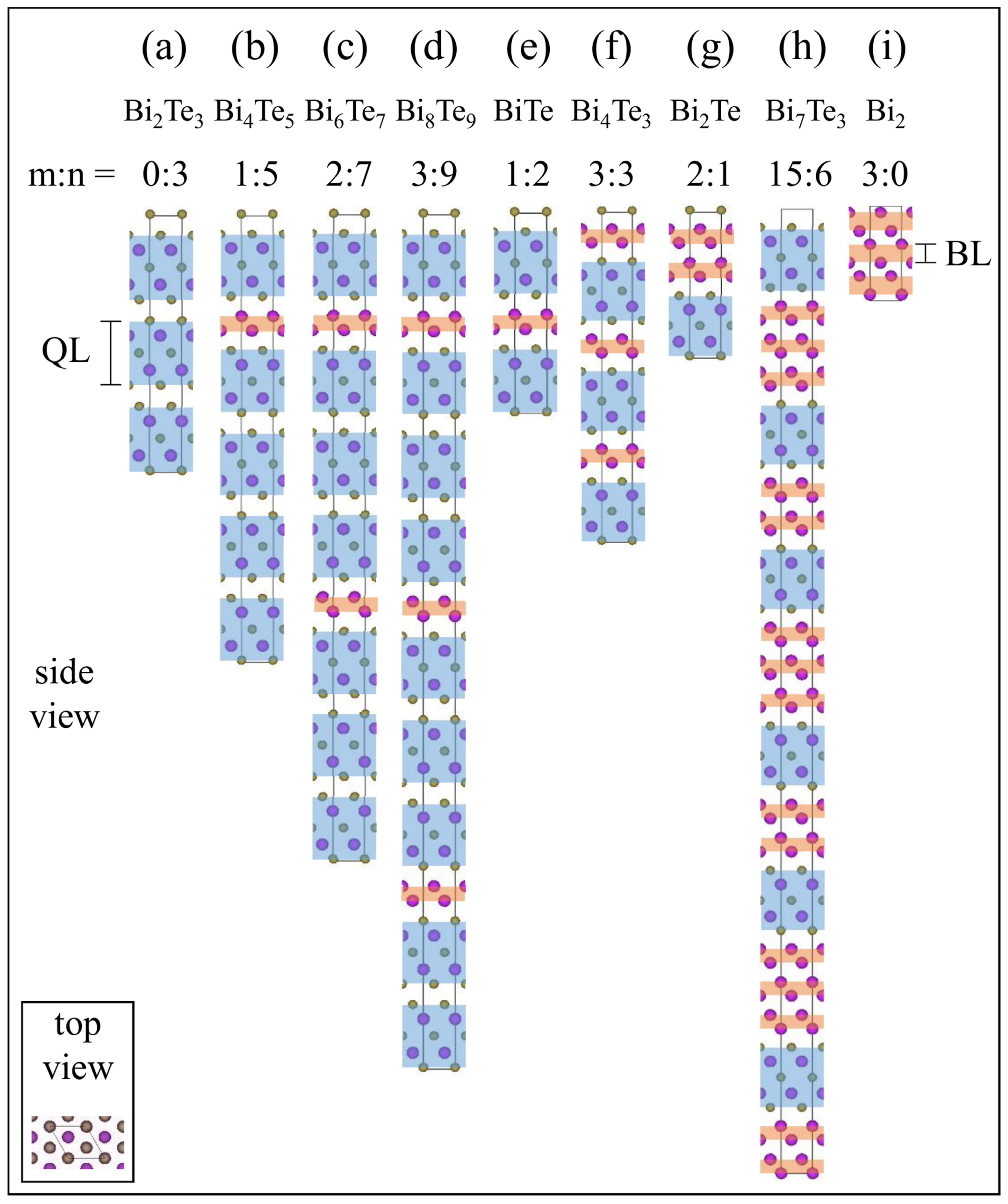
Figure 1. Atomic structures of hexagonal (Bi2)m(Bi2Te3)n: (a) Bi2Te3, (b) Bi4Te5, (c) Bi6Te7, (d) Bi8Te9, (e) BiTe, (f) Bi4Te3, (g) Bi2Te, (h) Bi7Te3, and (i) Bi2. The violet and gold balls indicate Bi and Te, respectively. The red and blue blocks display the Bi2 bilayer (BL) and Bi2Te3 quintuple layer (QL), respectively. The side and top view indicate the atomic structure seen from the vector direction of a and c in each respective (Bi2)m(Bi2Te3)n lattice.
Applsci 11 11341 g001
Figure 2. Layer mixing energy (EMixing) of (Bi2)m(Bi2Te3)n for (a) PBE and (b) LDA as a function of NBL/(NBL + NQL). The black dashed line shows EMixing for PBE, and the black line represents the EMixing for PBE with SOI (PBE + SOI), where the red solid and dashed lines indicate a convex hull of EMixing for PBE and PBE + SOI, respectively. The green dashed line displays EMixing for LDA, and the green dashed line represents EMixing for LDA with SOI (LDA + SOI), where the red solid and dashed lines indicate the convex hull of EMixing for LDA and LDA + SOI.
Applsci 11 11341 g002
Figure 3. Electronic band structures with density of states along the k-point paths of M− Γ −K and L−A−H in hexagonal (Bi2)m(Bi2Te3)n: (a) Bi2Te3, (b) Bi4Te5, (c) Bi6Te7, (d) Bi8Te9, (e) BiTe, (f) Bi4Te3, (g) Bi2Te, (h) Bi7Te3, and (i) Bi2. All band structures were obtained using DFT calculations with PBE.
Applsci 11 11341 g003
Figure 4. Electronic band structures with the density of states along the k-point paths of M− Γ −K and L−A−H in hexagonal (Bi2)m(Bi2Te3)n: (a) Bi2Te3, (b) Bi4Te5, (c) Bi6Te7, (d) Bi8Te9, (e) BiTe, (f) Bi4Te3, (g) Bi2Te, (h) Bi7Te3, and (i) Bi2. All band structures were obtained by using DFT calculations with PBE including SOI.
Applsci 11 11341 g004
Figure 5. Electronic band structures with density of states along the k-point path of M− Γ −K and L−A−H in hexagonal (Bi2)m(Bi2Te3)n: (a) Bi2Te3, (b) Bi4Te5, (c) Bi6Te7, (d) Bi8Te9, (e) BiTe, (f) Bi4Te3, (g) Bi2Te, (h) Bi7Te3, and (i) Bi2. All band structures were obtained by using DFT calculations with LDA.
Applsci 11 11341 g005
Figure 6. Electronic band structures with density of states along the k-point path of M− Γ −K and L−A−H in hexagonal (Bi2)m(Bi2Te3)n: (a) Bi2Te3, (b) Bi4Te5, (c) Bi6Te7, (d) Bi8Te9, (e) BiTe, (f) Bi4Te3, (g) Bi2Te, (h) Bi7Te3, and (i) Bi2. All band structures were obtained by using DFT calculations with LDA including SOI.
Applsci 11 11341 g006
Table 1. Phase properties, structural parameters, intralayer thickness, and interlayer distance of (Bi2)m(Bi2Te3)n homologous series depending on the Exc used for our calculations.
Chemical FormulaBi2Te3Bi4Te5Bi6Te7Bi8Te9BiTeBi4Te3Bi2TeBi7Te3Bi2
Phase
properties
Hexagonal
compositions
Bi6Te9Bi12Te15Bi18Te21Bi24Te27Bi6Te6Bi12Te9Bi6Te3Bi42Te18Bi6
NBL: NQL0:31:52:73:91:23:32:115:63:0
NBL/(NBL + NQL)00.1670.2220.2500.3330.5000.6670.7141
Structural parametersVolume/NAtom (Å3)33.89233.97433.98634.01533.88734.22435.09334.35235.383
aHex (Å)4.3884.4154.4244.4104.4234.4514.4904.4724.546
cHex (Å)30.48854.33078.200103.00024.00241.89018.090119.00011.862
cHex/NAtom (Å)2.0332.0122.0052.0202.0001.9952.0101.9831.977
PBEw/o
SOI
Intralayer thickness (Å)BL-1.6971.6931.7011.6921.6811.6711.6741.977
QL7.5297.4727.4537.4927.449 7.4157.3907.358-
Interlayer distance (Å)BL-BL------2.4642.3751.977
BL-QL-2.4362.4282.4532.4212.4342.4472.363-
QL-QL2.6342.6002.5862.6262.570----
w/
SOI
Intralayer thickness (Å)BL-1.7581.7531.7621.7481.7291.7041.7021.977
QL7.6237.5607.5387.5797.5257.4807.4547.409-
Interlayer distance (Å)BL-BL------2.4682.3751.977
BL-QL-2.4122.4002.4232.3862.3772.3802.303-
QL-QL2.5392.4882.4652.4942.433----
LDAw/o
SOI
Intralayer thickness (Å)BL-1.6611.6571.661.6571.6451.6321.6381.977
QL7.4547.4037.3847.4197.3837.3467.3107.291-
Interlayer distance (Å)BL-BL------2.5252.4261.977
BL-QL-2.4742.4692.4922.4672.4862.4952.404-
QL-QL2.7092.6772.6632.7142.645----
w/
SOI
Intralayer thickness (Å)BL-1.7181.7141.7221.7101.6931.6611.6611.977
QL7.5657.5097.4897.5267.4767.4217.3817.345-
Interlayer distance (Å)BL-BL------2.5492.4391.977
BL-QL-2.4662.4502.4762.4342.4252.4192.338-
QL-QL2.5982.5342.5102.5402.471----
Table 2. Determination of electric transport types (Type) of (Bi2)m(Bi2Te3)n from the energy gap in electronic band structure depending on the exclusion (X) and inclusion (O) of SOI using the Exc of PBE. EVBM and ECBM are the energy of VBM and CBM relative to the Fermi level of each (Bi2)m(Bi2Te3)n, respectively. E gap i and E gap d are the indirect and direct energy gaps, respectively. kVBM, kCBM, and k gap d are reciprocal positions of VBM, CBM, and E gap d in the first Brillouin zone, respectively. SC and SM represent semiconductors and semimetals, respectively.
ExcPhaseSOIEVBMkVBMECBMkCBM E g a p i E g a p d k g a p d Type
PBEBi2Te3X−0.1360.000 0.000 0.0000.1360.000 0.000 0.0000.2720.2720.000 0.000 0.000SC
O−0.0610.140 0.000 0.5000.0680.090 0.000 0.0000.1290.1350.130 0.000 0.500SC
Bi4Te5X0.0060.033 0.033 0.500−0.0590.000 0.000 0.500−0.0650.0050.010 0.000 0.500SM
O0.0120.170 0.000 0.000−0.0350.090 0.000 0.000−0.0470.0040.010 0.000 0.500SM
Bi6Te7X0.0020.033 0.033 0.000−0.0430.007 0.007 0.000−0.0450.0290.020 0.000 0.000SM
O0.0060.180 0.000 0.500−0.0180.000 0.000 0.500−0.0240.0080.020 0.000 0.000SM
Bi8Te9X−0.0040.033 0.033 0.500−0.0300.007 0.007 0.500−0.0260.0270.020 0.000 0.500SM
O0.0010.170 0.000 0.500−0.0190.000 0.000 0.500−0.0200.0010.000 0.000 0.500SM
BiTeX0.0170.060 0.000 0.000−0.0230.013 0.013 0.500−0.0400.0350.060 0.000 0.000SM
O−0.0640.180 0.000 0.5000.0530.027 0.027 0.5000.1170.1520.040 0.000 0.500SC
Bi4Te3X0.0300.110 0.000 0.000−0.0360.027 0.027 0.500−0.0660.0210.027 0.027 0.500SM
O0.1080.000 0.000 0.000−0.0840.500 0.000 0.000−0.1920.0010.020 0.000 0.000SM
Bi2TeX0.0250.067 0.067 0.000−0.0510.033 0.033 0.000−0.0760.0380.033 0.033 0.000SM
O0.1380.000 0.000 0.000−0.0410.500 0.000 0.500−0.1790.0300.030 0.000 0.000SM
Bi7Te3X0.0770.150 0.000 0.500−0.0680.027 0.027 0.500−0.1450.0210.027 0.027 0.500SM
O0.0410.000 0.000 0.500−0.0930.500 0.000 0.500−0.1340.0250.020 0.020 0.500SM
Bi2X0.0660.047 0.047 0.500−0.1970.480 0.000 0.500−0.2630.0200.047 0.047 0.500SM
O0.1130.000 0.000 0.500−0.0480.500 0.000 0.500−0.1610.0790.500 0.000 0.500SM
Table 3. Determination of electric transport type (Type) of (Bi2)m(Bi2Te3)n from the energy gap in the electronic band structure depending on the exclusion (X) and inclusion (O) of SOI using the Exc of LDA. EVBM and ECBM are the energy of VBM and CBM relative to the Fermi level of each (Bi2)m(Bi2Te3)n, respectively. E gap i and E gap d are the indirect and direct energy gaps, respectively. kVBM, kCBM, and k gap d are reciprocal positions of VBM, CBM, and E gap d in the first Brillouin zone, respectively. SC and SM represent semiconductors and semimetals, respectively.
ExcPhaseSOIEVBMkVBMECBMkCBM E g a p i E g a p d k g a p d Type
LDABi2Te3X−0.0980.000 0.000 0.0000.0980.000 0.000 0.0000.1960.1960.000 0.000 0.000SC
O−0.0550.140 0.000 0.5000.0560.130 0.000 0.5000.1110.1150.130 0.000 0.500SC
Bi4Te5X0.0270.040 0.040 0.500−0.0780.007 0.007 0.500−0.1050.0170.007 0.007 0.500SM
O−0.0040.180 0.000 0.000−0.0280.090 0.000 0.000−0.0240.0050.000 0.000 0.500SM
Bi6Te7X0.0210.040 0.040 0.500−0.0570.020 0.000 0.000−0.0780.0070.013 0.013 0.000SM
O−0.0090.000 0.000 0.000−0.0130.100 0.000 0.000−0.0040.0060.010 0.000 0.000SM
Bi8Te9X−0.0040.070 0.000 0.500−0.0190.013 0.013 0.500−0.0150.0070.013 0.013 0.500SM
O−0.0050.000 0.000 0.000−0.0020.000 0.000 0.0000.0030.0030.000 0.000 0.000SC
BiTeX0.0240.060 0.000 0.000−0.0280.020 0.020 0.500−0.0520.0130.060 0.000 0.000SM
O−0.0620.060 0.000 0.0000.0480.027 0.027 0.5000.1100.1340.040 0.000 0.500SC
Bi4Te3X0.0250.110 0.000 0.000−0.0390.027 0.027 0.500−0.0640.0360.027 0.027 0.500SM
O0.0810.000 0.000 0.000−0.0770.500 0.000 0.000−0.1580.0010.020 0.000 0.500SM
Bi2TeX0.0440.067 0.067 0.000−0.0830.033 0.033 0.000−0.1270.0050.033 0.033 0.000SM
O0.1200.000 0.000 0.000−0.0450.500 0.000 0.500−0.1650.0210.020 0.000 0.000SM
Bi7Te3X0.0850.170 0.000 0.000−0.0680.033 0.033 0.500−0.1530.0100.033 0.033 0.500SM
O0.0410.000 0.000 0.000−0.0950.500 0.000 0.500−0.1360.0090.000 0.000 0.000SM
Bi2X0.0730.053 0.053 0.500−0.2070.500 0.000 0.500−0.2800.0110.500 0.000 0.500SM
O0.0760.000 0.000 0.500−0.0380.500 0.000 0.500−0.1140.0890.500 0.000 0.500SM
Publisher’s Note: MDPI stays neutral with regard to jurisdictional claims in published maps and institutional affiliations.

