
Icing Mitigation by MEMS-Fabricated Surface Dielectric Barrier Discharge

 , and
, and
Abstract
:1. Introduction
2. SDBD Preparation
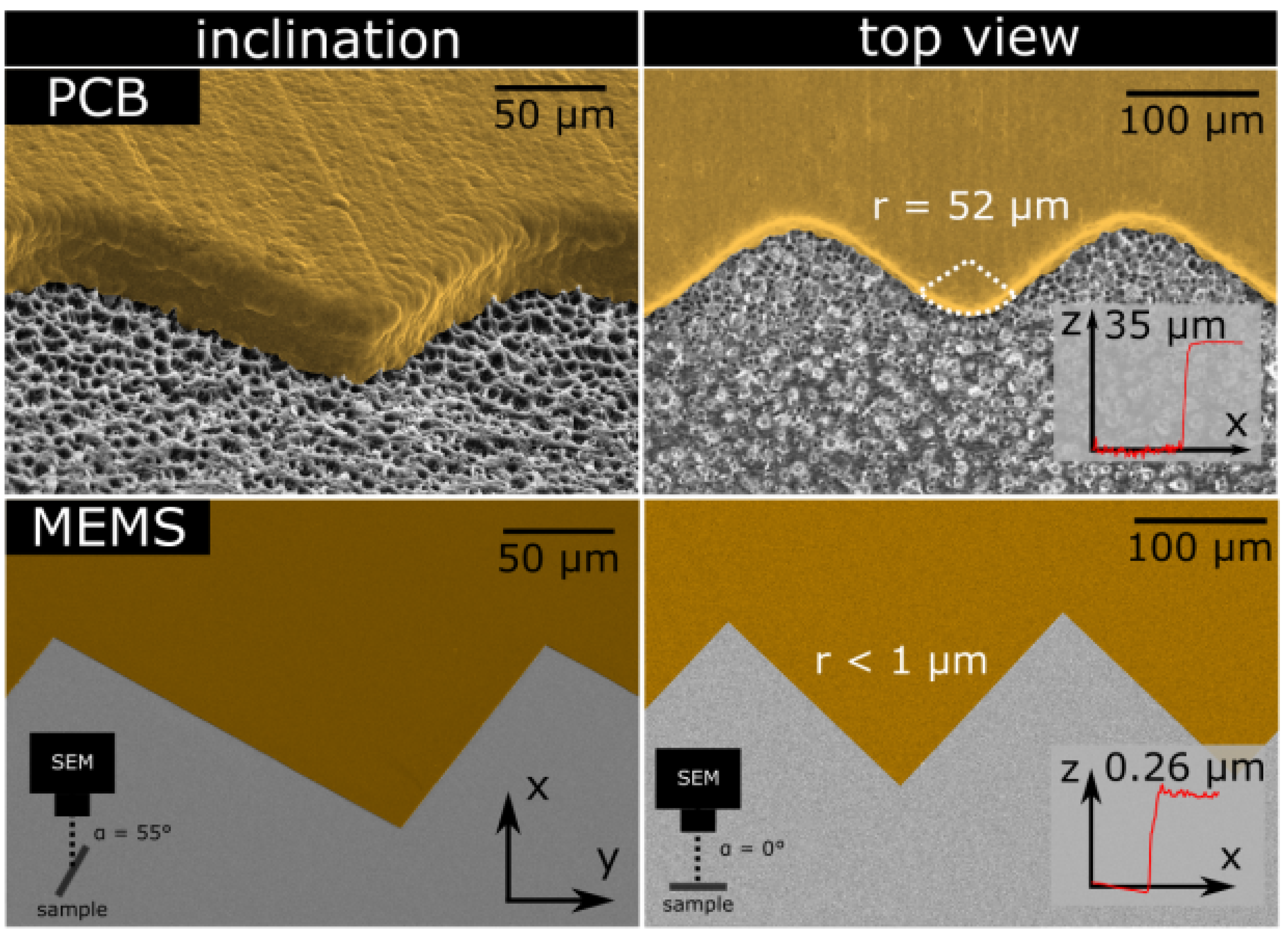
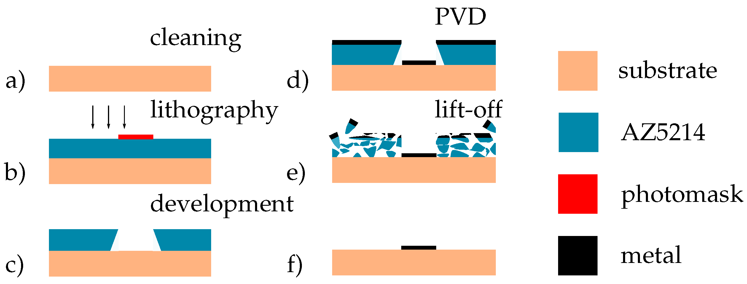
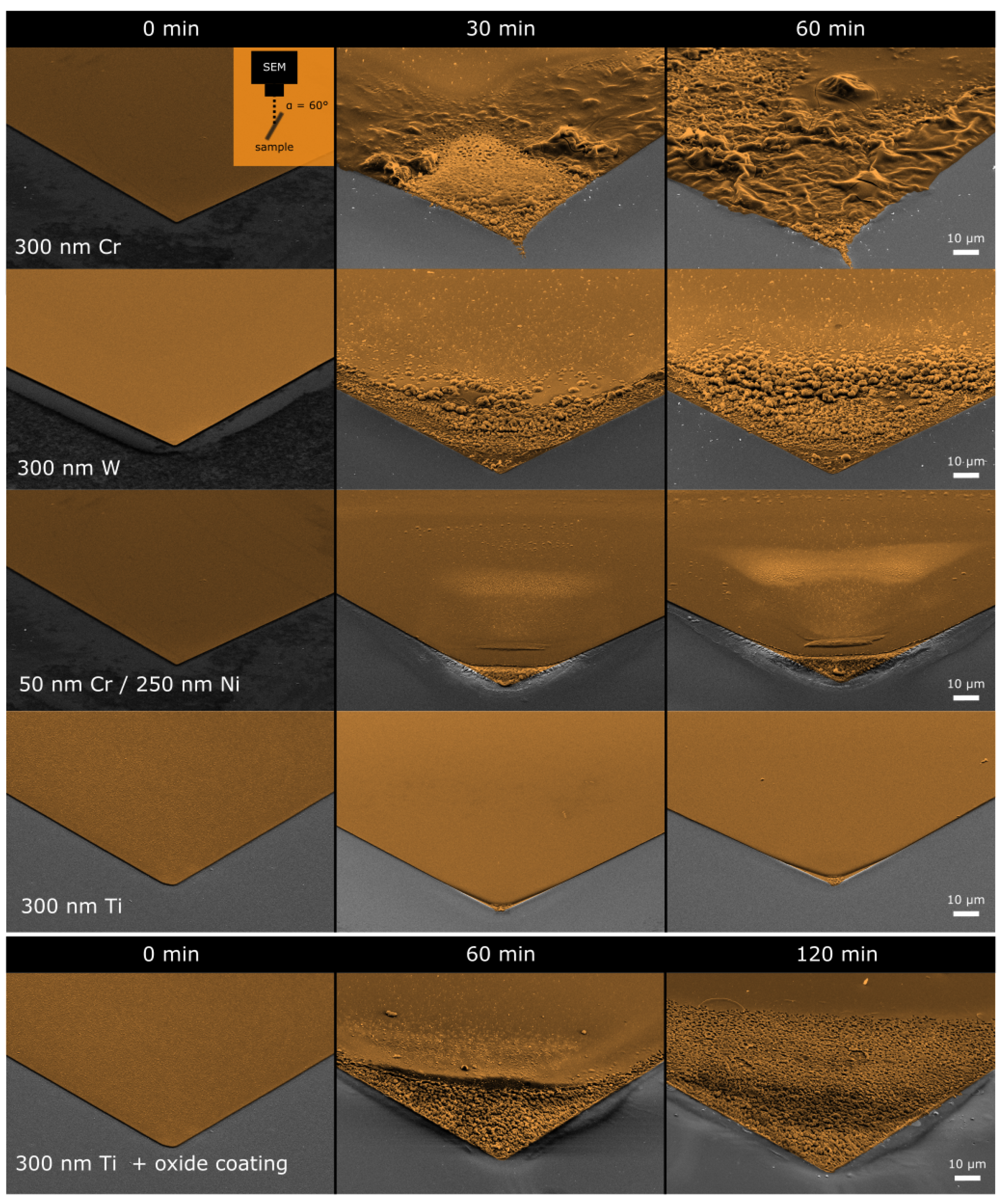
2.1. MEMS Fabrication
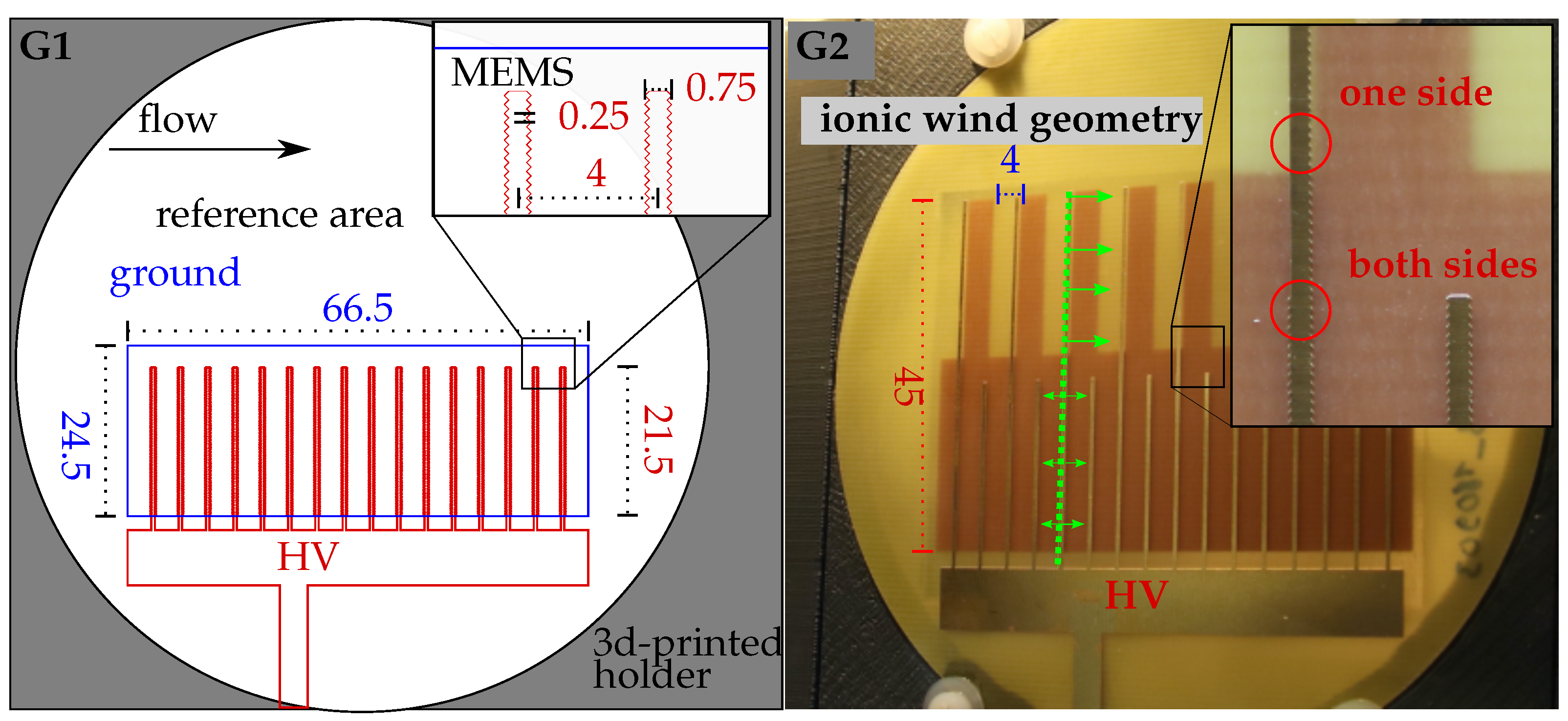
2.2. Geometry and Sample Preparation
3. Electrical Characterization
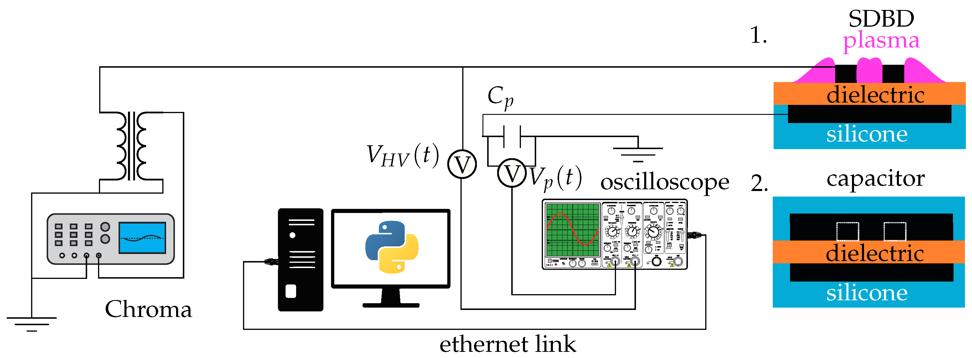
3.1. Setup
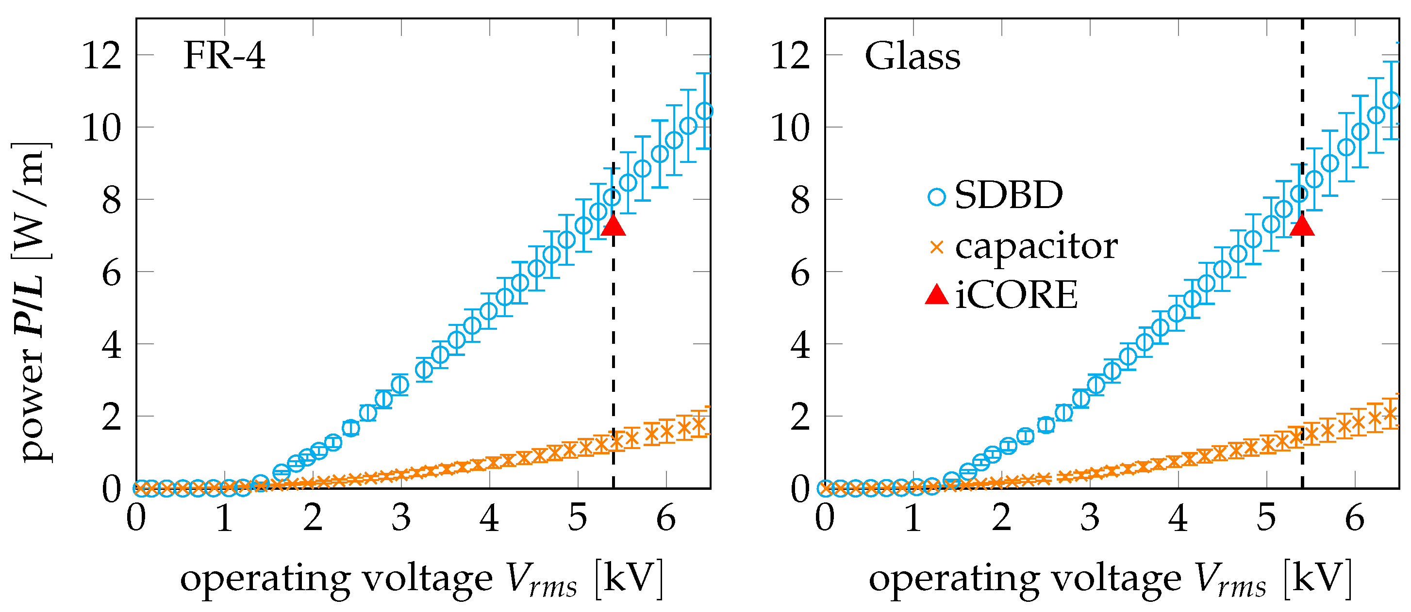
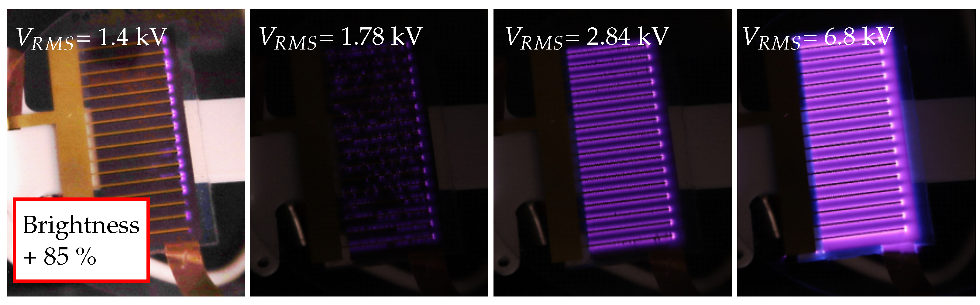
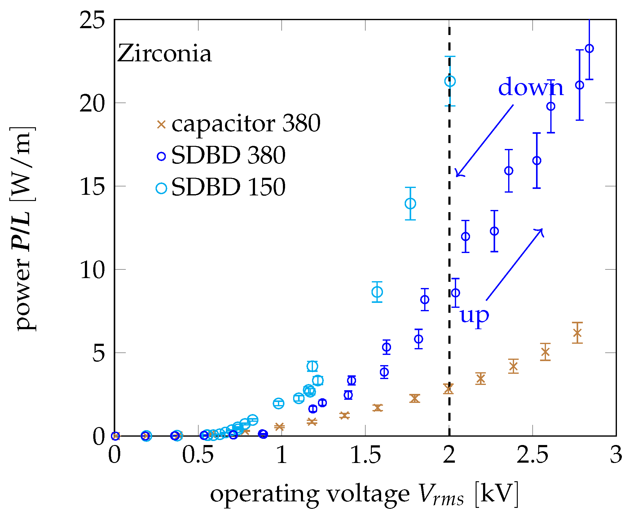
3.2. SDBD Power
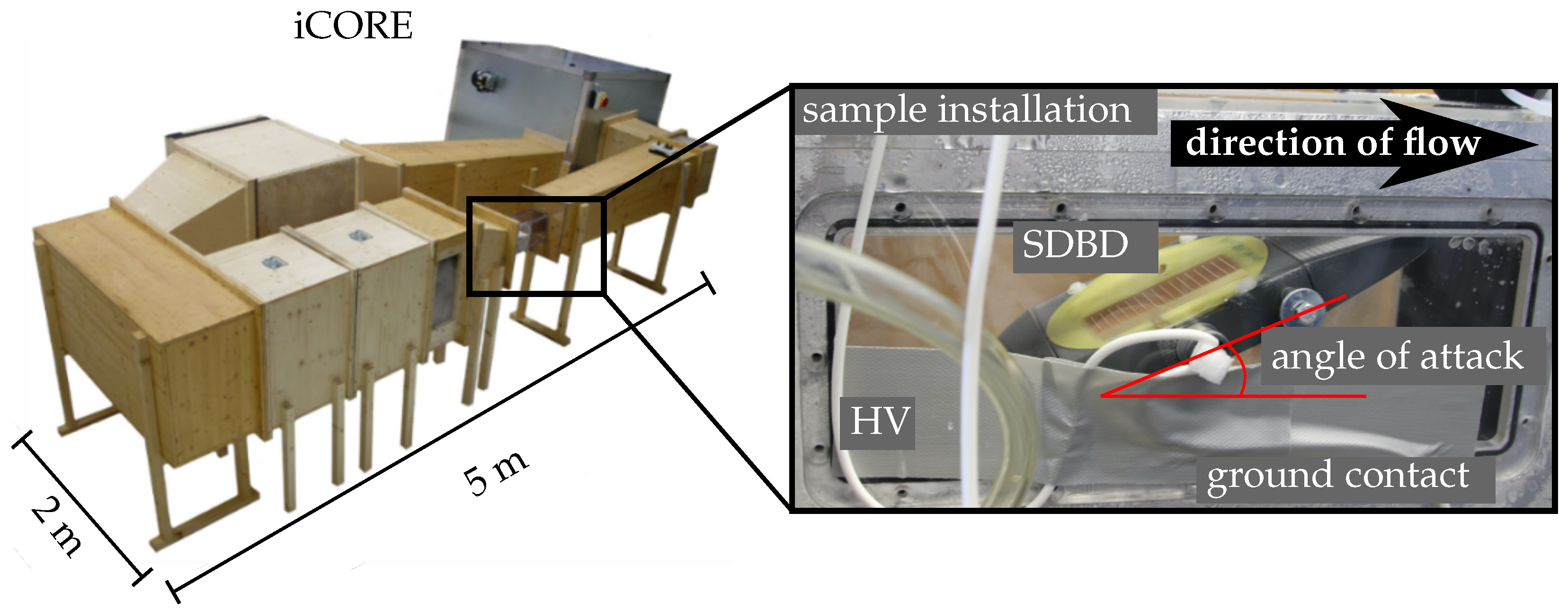
4. Icing Experiment
4.1. Setup
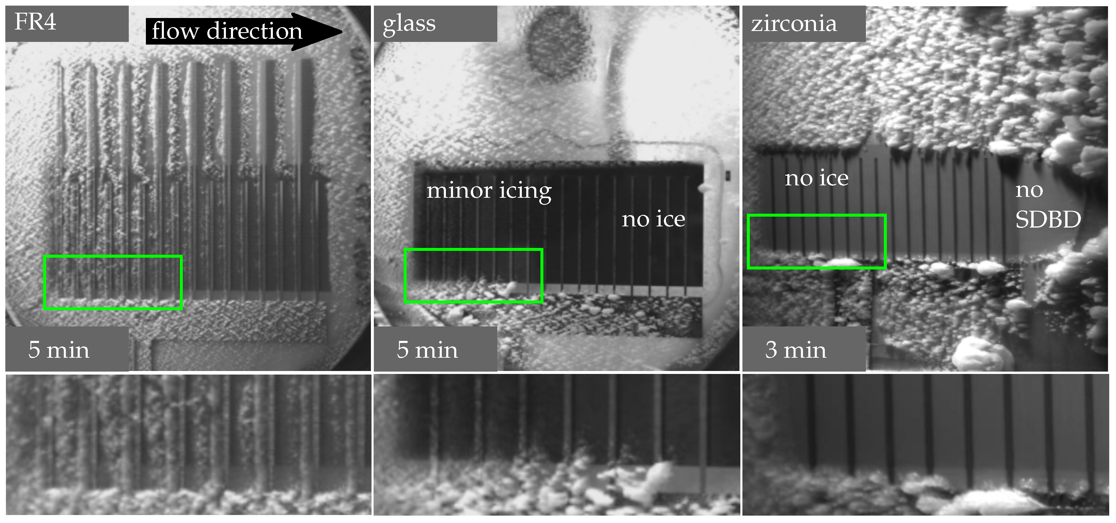
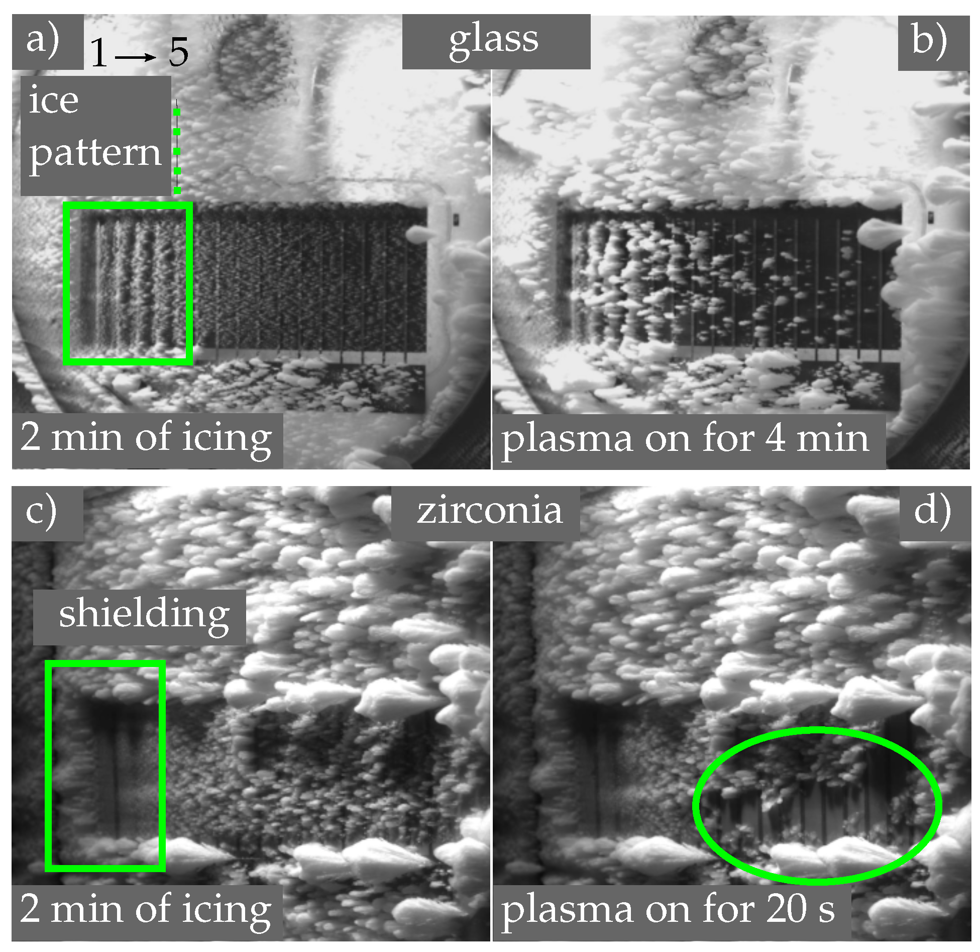
4.2. Anti-Icing Results
4.3. De-Icing Results
5. SDBD Efficiency
6. Summary
Supplementary Materials
Author Contributions
Funding
Institutional Review Board Statement
Acknowledgments
Conflicts of Interest
Sample Availability
Abbreviations
| ABS | Acrylonitrile Butadiene Styrene |
| EB-PVD | Electron Beam Physical Vapor Deposition |
| iCORE | Icing and Contamination Research facility |
| LWC | Liquid Water Content |
| MEMS | Micro Electro Mechanical Systems |
| MVD | Median Volumetric Diameter |
| PCB | Printed Circuit Board |
| PA | Plasma Actuator |
| RMS | Root Mean Square |
| SDBD | Surface Dielectric Barrier Discharge |
| SEM | Scanning Electron Microscope |
References
- Bragg, M. Effect of geometry on airfoil icing characteristics. J. Aircr. 1984, 21, 505–511. [Google Scholar] [CrossRef]
- Vercillo, V.; Karpen, N.; Laroche, A.; Guillén, J.; Tonnicchia, S.; Andrade Jorge, R.; Bonaccurso, E. Analysis and modelling of icing of air intake protection grids of aircraft engines. Cold Reg. Sci. Technol. 2019, 160, 265–272. [Google Scholar] [CrossRef]
- Thomas, S.; Cassoni, R.; MacArthur, C. Aircraft anti-icing and de-icing techniques and modeling. J. Aircr. 1996, 33, 841–854. [Google Scholar] [CrossRef]
- Drury, M.; Szefi, J.; Palacios, J. Full-scale testing of a centrifugally powered pneumatic de-icing system for helicopter rotor blades. J. Aircr. 2017, 54, 220–228. [Google Scholar] [CrossRef]
- Blaha, B.; Evanich, P. Pneumatic Boot for Helicopter Rotor Deicing; National Aeronautics: Washington, DC, USA, 1981. [Google Scholar]
- Dong, W.; Zhu, J.; Zheng, M.; Chen, Y. Thermal analysis and testing of nonrotating cone with hot-air anti-icing system. J. Propuls. Power 2015, 31, 896–903. [Google Scholar] [CrossRef]
- Al-Khalil, K. Thermo-Mechanical Expulsive Deicing System-TMEDS. In Proceedings of the 45th AIAA Aerospace Sciences Meeting Furthermore, Exhibit, Reno, NV, USA, 8–11 January 2007; p. 692. [Google Scholar]
- Vertuccio, L.; De Santis, F.; Pantani, R.; Lafdi, K.; Guadagno, L. Effective de-icing skin using graphene-based flexible heater. Compos. Part Eng. 2019, 162, 600–610. [Google Scholar] [CrossRef]
- Lai, C.; Fu, H.; Hu, B.; Ling, Z.; Jiang, L. Aerodynamic Drag Reduction and Optimization of MIRA Model Based on Plasma Actuator. Actuators 2020, 9, 64. [Google Scholar] [CrossRef]
- Lo, K.; Sriram, R.; Kontis, K. Wake Flow Characteristics over an Articulated Lorry Model with/without AC-DBD Plasma Actuation. Appl. Sci. 2019, 9, 2426. [Google Scholar] [CrossRef] [Green Version]
- Chen, J.; Liang, H.; Wu, Y.; Wei, B.; Zhao, G.; Tian, M.; Xie, L. Experimental Study on Anti-Icing Performance of NS-DBD Plasma Actuator. Appl. Sci. 2018, 8, 1889. [Google Scholar] [CrossRef] [Green Version]
- Yu, J.; Yu, J.; Chen, F.; Wang, C. Numerical study of tip leakage flow control in turbine cascades using the DBD plasma model improved by the parameter identification method. Aerosp. Sci. Technol. 2019, 84, 856–864. [Google Scholar] [CrossRef]
- Abdollahzadeh, M.; Pascoa, J.; Oliveira, P. Comparison of DBD plasma actuators flow control authority in different modes of actuation. Aerosp. Sci. Technol. 2018, 78, 183–196. [Google Scholar] [CrossRef]
- Ebrahimi, A.; Hajipour, M. Flow separation control over an airfoil using dual excitation of DBD plasma actuators. Aerosp. Sci. Technol. 2018, 79, 658–668. [Google Scholar] [CrossRef]
- Kriegseis, J.; Simon, B.; Grundmann, S. Towards in-flight applications? A review on dielectric barrier discharge-based boundary-layer control. Appl. Mech. Rev. 2016, 68, 020802. [Google Scholar] [CrossRef]
- Pescini, E.; De Giorgi, M.; Suma, A.; Francioso, L.; Ficarella, A. Separation control by a microfabricated SDBD plasma actuator for small engine turbine applications: Influence of the excitation waveform. Aerosp. Sci. Technol. 2018, 76, 442–454. [Google Scholar] [CrossRef]
- Sato, S.; Enokido, T.; Ashikawa, K.; Matsubara, M.; Kanie, K.; Ohnishi, N. Development of a flexible dielectric-barrier-discharge plasma actuator fabricated by inkjet printing using silver nanoparticles-based ink. Sens. Actuators Phys. 2021, 2021, 112823. [Google Scholar] [CrossRef]
- Rodrigues, F.; Abdollahzadeh, M.; Pascoa, J.; Oliveira, P. An Experimental Study on Segmented-Encapsulated Electrode Dielectric-Barrier-Discharge Plasma Actuator for Mapping Ice Formation on a Surface: A Conceptual Analysis. J. Heat Transf. 2021, 143, 011701. [Google Scholar] [CrossRef]
- Benmoussa, A.; Páscoa, J. Cycloidal rotor coupled with DBD plasma actuators for performance improvement. Aerosp. Sci. Technol. 2021, 110, 106468. [Google Scholar] [CrossRef]
- Baranov, S.; Chernyshev, S.; Khomich, V.; Kiselev, A.; Kuryachii, A.; Moshkunov, S.; Rebrov, I.; Sboev, D.; Tolkachev, S.; Yamshchikov, V. Experimental cross-flow control in a 3D boundary layer by multi-discharge plasma actuators. Aerosp. Sci. Technol. 2021, 112, 106643. [Google Scholar] [CrossRef]
- Cai, J.; Tian, Y.; Meng, X.; Han, X.; Zhang, D.; Hu, H. An experimental study of icing control using DBD plasma actuator. Exp. Fluids 2017, 58, 1–8. [Google Scholar] [CrossRef]
- Yongqiang, T.; Zhang, Z.; Jinsheng, C.; Leilei, Y.; Lei, K. Experimental study of an anti-icing method over an airfoil based on pulsed dielectric barrier discharge plasma. Chin. J. Aeronaut. 2018, 31, 1449–1460. [Google Scholar]
- Meng, X.; Hu, H.; Li, C.; Abbasi, A.; Cai, J.; Hu, H. Mechanism study of coupled aerodynamic and thermal effects using plasma actuation for anti-icing. Phys. Fluids 2019, 31, 037103. [Google Scholar] [CrossRef] [Green Version]
- Meng, X.; Cai, J.; Tian, Y.; Han, X.; Zhang, D. Experimental Study of Anti-icing and Deicing on a Cylinder by DBD plasma actuation. In Proceedings of the 47th AIAA Plasmadynamics and Lasers Conference, Washington, DC, USA, 13–17 June 2016; p. 4019. [Google Scholar]
- Kolbakir, C.; Hu, H.; Liu, Y.; Hu, H. An experimental study on different plasma actuator layouts for aircraft icing mitigation. Aerosp. Sci. Technol. 2012, 107, 106325. [Google Scholar] [CrossRef]
- Chen, Z. A Phenomenon Study on Spreading and Evaporating Process of Droplet on DBD Actuator for Wind Turbine Anti-icing. IOP Conf. Ser. Earth Environ. Sci. 2020, 453, 012049. [Google Scholar] [CrossRef]
- Wei, B.; Wu, Y.; Liang, H.; Zhu, Y.; Chen, J.; Zhao, G.; Song, H.; Jia, M.; Xu, H. SDBD based plasma anti-icing: A stream-wise plasma heat knife configuration and criteria energy analysis. Int. J. Heat Mass Transf. 2019, 138, 163–172. [Google Scholar] [CrossRef]
- Lindner, M.; Berndt, D.; Tschurtschenthaler, K.; Ehrlich, I.; Jungbauer, B.; Schreiner, R.; Pipa, A.; Hink, R.; Foest, R.; Brandenburg, R.; et al. Aircraft Icing Mitigation by DBD-based Micro Plasma Actuators. In AIAA Aviation 2020 Forum; AIAA: Reston, VA, USA, 2020; p. 3243. [Google Scholar]
- Gao, T.; Luo, Z.; Zhou, Y.; Yang, S. A novel de-icing strategy combining electric-heating with plasma synthetic jet actuator. Proc. Inst. Mech. Eng. Part J. Aerosp. Eng. 2021, 235, 513–522. [Google Scholar] [CrossRef]
- Niu, J.; Sang, W.; Zhou, F.; Li, D. Numerical investigation of an anti-icing method on airfoil based on the NSDBD plasma actuator. Aircr. Eng. Aerosp. Technol. 2021, 93. [Google Scholar] [CrossRef]
- Rodrigues, F.; Pascoa, J.; Trancossi, M. Heat generation mechanisms of DBD plasma actuators. Exp. Therm. Fluid Sci. 2018, 90, 55–65. [Google Scholar] [CrossRef] [Green Version]
- Lindner, M.; Berndt, D.; Ehrlich, I.; Jungbauer, B.; Schreiner, R.; Pipa, A.; Hink, R.; Foest, R.; Brandenburg, R.; Max, A.; et al. Fabrication, surface integration and testing of miniaturized dielectric barrier discharge plasma actuators for active flow control applications. In AIAA Aviation 2019 Forum; AIAA: Reston, VA, USA, 2019; p. 2998. [Google Scholar]
- Houser, N.; Gimeno, L.; Hanson, R.; Goldhawk, T.; Simpson, T.; Lavoie, P. Microfabrication of dielectric barrier discharge plasma actuators for flow control. Sens. Actuators Phys. 2013, 201, 101–104. [Google Scholar] [CrossRef]
- Hink, R.; Pipa, A.; Schaefer, J.; Caspari, R.; Weichwald, R.; Foest, R.; Brandenburg, R. Influence of dielectric thickness and electrode structure on the ion wind generation by micro fabricated plasma actuators. J. Phys. Appl. Phys. 2020, 53, 405201. [Google Scholar] [CrossRef]
- Okochi, S.; Kasagi, N.; Suzuki, Y.; Ito, S. Development of micro plasma actuator for active flow control. In Proceedings of the 7th World Conference On Experimental Heat Transfer, Fluid Mechanics, Furthermore, Thermodynamics, Krakow, Poland, 28 June–3 July 2009. [Google Scholar]
- Durscher, R.; Roy, S. Three-dimensional flow measurements induced from serpentine plasma actuators in quiescent air. J. Phys. Appl. Phys. 2012, 45, 035202. [Google Scholar] [CrossRef]
- Pescini, E.; De Giorgi, M.; Francioso, L.; Taurino, A.; Martucci, M.; Lavoie, P. Electrode material degradation monitoring for durable dielectric barrier discharge plasma actuators manufacturing. In Proceedings of the 54th AIAA Aerospace Sciences Meeting, San Diego, CA, USA, 4–8 January 2016; p. 0196. [Google Scholar]
- Pons, J.; Oukacine, L.; Moreau, E.; Tatibouet, J. Observation of dielectric degradation after surface dielectric barrier discharge operation in air at atmospheric pressure. IEEE Trans. Plasma Sci. 2008, 36, 1342–1343. [Google Scholar] [CrossRef]
- Berndt, D.; Lindner, M.; Schreiner, R.; Hink, R.; Pipa, A.; Schaefer, J.; Brandenburg, R.; Foest, R.; Geils, J.; Sander, A.; et al. Realization of Multifunctional Surfaces Containing MEMS-based DBD Plasma Actuators and Biomimetic Structures for Flow Manipulation. In AIAA Aviation 2019 Forum; AIAA: Reston, VA, USA, 2019; p. 2999. [Google Scholar]
- Pipa, A.; Brandenburg, R. The equivalent circuit approach for the electrical diagnostics of dielectric barrier discharges: The classical theory and recent developments. Atoms 2019, 7, 14. [Google Scholar] [CrossRef] [Green Version]
- Manley, T. The electric characteristics of the ozonator discharge. Trans. Electrochem. Soc. 1943, 84, 83. [Google Scholar] [CrossRef]
- Piferi, C.; Barni, R.; Roman, H.; Riccardi, C. Current Filaments in Asymmetric Surface Dielectric Barrier Discharge. Appl. Sci. 2021, 11, 2079. [Google Scholar] [CrossRef]
- Pipa, A.; Hink, R.; Foest, R.; Brandenburg, R. Dependence of dissipated power on applied voltage for surface barrier discharge from simplest equivalent circuit. Plasma Sources Sci. Technol. 2020, 29, 12LT01. [Google Scholar] [CrossRef]
- Scherrer, B.; Schlupp, M.; Stender, D.; Martynczuk, J.; Grolig, J.; Ma, H.; Kocher, P.; Lippert, T.; Prestat, M.; Gauckler, L. On proton conductivity in porous and dense yttria stabilized zirconia at low temperature. Adv. Funct. Mater. 2013, 23, 1957–1964. [Google Scholar] [CrossRef]
- Schott Schott Borofloat33. 2021. Available online: https://www.metaglas.de/fileadmin/dokumente/pdf/LGS-Borofloat.pdf (accessed on 19 October 2021).
- WE Datenblatt Standard FR4 TG135. 2021. Available online: https://www.wedirekt.de/.../FR4TG135_DE.pdf (accessed on 19 October 2021).
- Hauk, T.; Strobl, T.; Raps, D. Implementation and calibration of the icing and contamination research facility (iCORE). In Proceedings of the ILASS-Europe, 25th European Conference on Liquid Atomization Furthermore Spray Systems, Chania, Greece, 1–4 September 2013; Volume 1. [Google Scholar]
- Vercillo, V. Durable Laser Patterned Metal Surfaces with Enhanced Icephobic Properties for Aerospace Applications. Ph.D. Thesis, Technische Universität Dresden, Dresden, Germany, 2020. [Google Scholar]
- Makkonen, L. Models for the growth of rime, glaze, icicles and wet snow on structures. Philos. Trans. R. Soc. London. Ser. Math. Phys. Eng. Sci. 2000, 358, 2913–2939. [Google Scholar] [CrossRef]
- Momen, G.; Jafari, R.; Farzaneh, M. Ice repellency behaviour of superhydrophobic surfaces: Effects of atmospheric icing conditions and surface roughness. Appl. Surf. Sci. 2015, 349, 211–218. [Google Scholar] [CrossRef]
- Roisman, I.; Rioboo, R.; Tropea, C. Normal impact of a liquid drop on a dry surface: Model for spreading and receding. Proc. R. Soc. London. Ser. Math. Phys. Eng. Sci. 2002, 458, 1411–1430. [Google Scholar] [CrossRef]
- Jacobi, A.; Shah, R. Heat transfer surface enhancement through the use of longitudinal vortices: A review of recent progress. Exp. Therm. Fluid Sci. 1995, 11, 295–309. [Google Scholar] [CrossRef]
- Zheng, M.; Dong, W.; Guo, Z.; Lei, G. Analysis of Runback Water Flow on Anti-Icing Surface Using Volume-of-Fluid Method. In Proceedings of the Turbo Expo: Power for Land, Sea, and Air, Charlotte, NC, USA, 26 June 2017; p. 50879. [Google Scholar]
- Hui, M.; Dalin, Z.; Fanxin, M. Others Experiment of Electro-thermal Anti-icing on a Composite Assembly. Acta Aeronaut. Astronaut. Sin. 2013, 34, 8. [Google Scholar]
- Fortin, G.; Adomou, M.; Perron, J. Experimental Study of Hybrid Anti-Icing Systems Combining Thermoelectric and Hydrophobic Coatings; SAE Technical Paper; SAE: Warrendale, PA, USA, 2011. [Google Scholar]
- Küchler, A. Hochspannungstechnik; Springer: Berlin/Heidelberg, Germany, 2009. [Google Scholar]
- Roth, J.; Sin, H.; Madhan, R.; Wilkinson, S. Flow re-attachment and acceleration by paraelectric and peristaltic electrohydrodynamic (EHD) effects. In Proceedings of the 41st Aerospace Sciences Meeting Furthermore, Exhibit, Reno, NV, USA, 6–9 January 2003; p. 531. [Google Scholar]
- Smielak, B.; Klimek, L.; Wojciechowski, R.; Bąkała, M. Effect of zirconia surface treatment on its wettability by liquid ceramics. J. Prosthet. Dent. 2019, 122, e1–e6. [Google Scholar] [CrossRef]


| Substrate Properties | Electrodes | iCORE | ||||||||||
|---|---|---|---|---|---|---|---|---|---|---|---|---|
| Name | σ [μm] | ϵr | Θ | tan δ | ddiel [μm] | Method | del [μm] | Metal | Vrms [kV] | P/L [W/m] | v [m/s] | T [°C] |
| FR-4 | 0.70 | 5.5 | 106° | 0.008 | 500 | PCB | 35 | Cu/Au | 5.4 | 7.2 ± 0.5 | 50 | −17 |
| Borofloat glass | 0.02 | 4.3 | 99° | 0.011 | 500 | MEMS | 0.26 | Cr/Ni | 5.4 | 7.2 ± 0.5 | 27 | −18 |
| Zirconia ceramic | 0.15 | 28.3 | 68° | 0.015 | 150 | MEMS | 0.2 | Ti | 2.0 | ∼20 * | 30 | −20 |
| Publication | Technology | Discharge Power [kW/m2] | System Power [kW/m2] | Temperature [°C] | Wind Speed [m/s] | LWC [g/m3] |
|---|---|---|---|---|---|---|
| Ma et al. [54] | heating device | − | 92 | −5 | 90 | 2 |
| Frotin et al. [55] | heating device | − | 62 | −5 & −20 | 21 | 0.4 |
| Tian et al. [22] | pulsed-SDBD, grid | 8.3 | 31 | −7 | 90 | 0.5 |
| Tian et al. [22] | pulsed-SDBD, stripes | 7.3 | 28 | −7 | 90 | 0.5 |
| current work | glass/PCB SDBD | 3.1 ± 0.3 | 19 ± 1 | −17.5 ± 1 | 27 & 50 | 3 |
| current work | zirconia SDBD | 8.9 ± 1 | 27 ± 2 | −20 | 30 | 3 |
Publisher’s Note: MDPI stays neutral with regard to jurisdictional claims in published maps and institutional affiliations. |
© 2021 by the authors. Licensee MDPI, Basel, Switzerland. This article is an open access article distributed under the terms and conditions of the Creative Commons Attribution (CC BY) license (https://creativecommons.org/licenses/by/4.0/).
Share and Cite
Lindner, M.; Pipa, A.V.; Karpen, N.; Hink, R.; Berndt, D.; Foest, R.; Bonaccurso, E.; Weichwald, R.; Friedberger, A.; Caspari, R.; et al. Icing Mitigation by MEMS-Fabricated Surface Dielectric Barrier Discharge. Appl. Sci. 2021, 11, 11106. https://doi.org/10.3390/app112311106
Lindner M, Pipa AV, Karpen N, Hink R, Berndt D, Foest R, Bonaccurso E, Weichwald R, Friedberger A, Caspari R, et al. Icing Mitigation by MEMS-Fabricated Surface Dielectric Barrier Discharge. Applied Sciences. 2021; 11(23):11106. https://doi.org/10.3390/app112311106
Chicago/Turabian StyleLindner, Matthias, Andrei V. Pipa, Norbert Karpen, Rüdiger Hink, Dominik Berndt, Rüdiger Foest, Elmar Bonaccurso, Robert Weichwald, Alois Friedberger, Ralf Caspari, and et al. 2021. "Icing Mitigation by MEMS-Fabricated Surface Dielectric Barrier Discharge" Applied Sciences 11, no. 23: 11106. https://doi.org/10.3390/app112311106
APA StyleLindner, M., Pipa, A. V., Karpen, N., Hink, R., Berndt, D., Foest, R., Bonaccurso, E., Weichwald, R., Friedberger, A., Caspari, R., Brandenburg, R., & Schreiner, R. (2021). Icing Mitigation by MEMS-Fabricated Surface Dielectric Barrier Discharge. Applied Sciences, 11(23), 11106. https://doi.org/10.3390/app112311106