Abstract
Usually, the residual layer remains after patterning TiO2 sol. The existence of the TiO2 residual layer in the non-pattern region affects its application in microelectronic devices. Here, a simple method, based on room-temperature imprinting, to fabricate a residual-free TiO2 pattern is proposed. The thermoplastic polymer with Ti4+ salt was fast patterned at room temperature by imprinting, based on the different interfacial force. Then, the patterned thermoplastic polymer with Ti4+ salt was induced into the TiO2 lines without residual layer under the hydrothermal condition. This method provides a new idea to pattern metal oxide without residual layer, which is potentially applied to the gas sensor, the optical detector and the light emitting diode.
1. Introduction
In the field of material micro-nano processing, the patterning technology has attracted more and more attention such as chemical vapor deposition [1], electrochemical machining [2], focused ion beam [3], imprinting [4] and so on. The imprinting method [5,6,7,8] is a new technology, which is famous for its high efficiency, large area and repeatability. However, the high-resolution template is expensive and is easily consumed in the imprinting process. The question of how to use the low-cost template to fabricate high-resolution patterns has aroused the attention of researchers.
In 1996, Whitesides first described that the filling material would gather to the edge of template channels in the process of imprinting, as there was not enough to completely fill the template, with the result that the obtained pattern would possess a higher resolution than the original template [9]. Inspired by this unconventional imprinting, scientists have made a lot of meaningful research achievements [10,11]. For example, Lee and Suh et al. used this method to construct thermoplastic and light-cured polymers with high resolution, which were applied to the biomimetic interfaces [12,13]. Xia et al. transferred organic small molecules to the edge of template channel by this method, which was as the etching barrier to fabricate high-resolution metal nanowires [14]. Cavallini et al. utilized capillary flow to fabricate high-resolution patterns of biomolecular and inorganic nanoparticles in the solvent evaporation process [15]. Han et al. combined Cavallini’s work to fabricate high-resolution patterns of thermoplastic polymers by capillary flow during solvent volatilization, avoiding high temperature and high pressure [16]. Titanium dioxide is an important functional material [17,18]. In the previous work of our group, a simple solvent-assisted soft lithography was introduced to fabricate high-resolution TiO2 patterns, which also utilized the capillary flow during solvent volatilization [19]. Although this method has many advantages in the fabrication of high-resolution patterns, it is very difficult to solve the problem of TiO2 residual layer during the imprinting process, which limits the application of this technology in the field of the gas sensor, the optical detector and the light emitting diode.
Here, the lines of thermoplastic polymer with Ti4+ salt were firstly fabricated by fast room-temperature imprinting (FRTI). After calcination, TiO2 was induced to assembly on the surface of patterns by hydrothermal reaction, resulting in the formation of TiO2 lines without residual layer. Meanwhile, the removal mechanism of TiO2 residual layer in the non-pattern region would be explained in detail, which has not yet been reported.
2. Materials and Methods
There are the following experiment materials. Chloroform, ethanol, acetone, hydrochloric acid (HCl), xylene and titanium n-butoxide [Ti(OC4H9)4] were of Guarantee Reagent level and did not need pre-purification before utilization (Beijing Chemical Reagent Plant). The Si wafers [p-type (100)] were received from Youyan Guigu Beijing, China. The poly-(methylmethacrylate) (PMMA) (molecular weight Mw = 75 kDa) was purchased from Microresist Technology GmbH, Berlin, Germany.
The fabrication of the PDMS template is as follows. The unpolymerized PDMS, composed of mixed prepolymer and initiator in a 10:1 ratio, was poured onto the structured photoresist. The PDMS template was then peeled off the structured photoresist after baking at 90 °C for 4 h.
The assembly of PMMA/Ti4+ on the PDMS surface is as follows. 0.5%, 1% and 1.5% of PMMA in the xylene was prepared respectively, into which Ti(C4H9O)4 was added at the mass ratio of 1 (Ti(C4H9O)4):13 (xylene solution for PMMA). The aforementioned solution of PMMA/Ti4+ was coated on the PDMS template by spinning the aforementioned solution, to obtain PMMA/Ti4+ film.
The fabrication of PMMA/Ti4+ lines is as follows. The PMMA/Ti4+ film on the PDMS template and the substrate were treated to obtain the surface hydroxyl groups by O2 Plasma. Then, the PDMS template with the hydroxylated PMMA/Ti4+ film was imprinted on the hydroxylated substrate for 5–180 s. After the PDMS template was lifted off the substrate, the PMMA/Ti4+ lines were obtained on the substrate.
The fabrication of TiO2 lines without residual layer is as follows. The substrate with PMMA/Ti4+ lines was calcined at 450 °C for 30 min and was then placed into the reaction vessel with the mixed solution of 10 mL H2O, 10 mL HCl (37%) and 0.5 mL TiCl4 at 130 °C for 4 h and 8 h [20]. The TiO2 lines without residual layer were finally fabricated.
The characterizations are as follows. Atomic force microscope (AFM, Bruker MuLtimode 8) was operated to test the surface topography of PMMA/Ti4+ lines by using silicon cantilevers with a resonant frequency 250–350 kHz. Scanning electron microscope (SEM, Hitachi S-4800) was operated to test the surface topography of TiO2 lines with voltage of 2.0 kV, working distance of 10 mm and high vacuum environment.
3. Results and Discussion
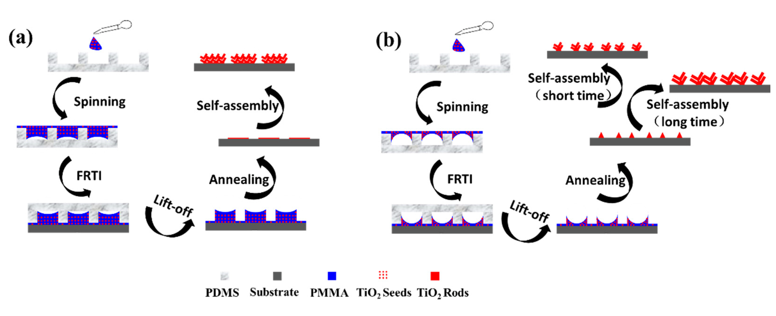
The scheme of fabricating TiO2 lines without residual layer is shown in Figure 1. Firstly, PMMA loaded with titanium salt (PMMA/Ti4+) in the xylene solution was spin-coated on the surface of PDMS template. In the spin-coating process, the solution is filled into the template by capillary force, forming the meniscus between air and liquid within the concave field [19,21,22,23]. Secondly, the hydroxyl was modified on the surface of the PMMA/Ti4+ film and the substrate by the O2 Plasma. Then, the PMMA/Ti4+ film deposited on the surface of PDMS was contacted with the substrate, and then was transferred to the substrate surface. The hydrogen bonding effect between the PMMA/Ti4+ film and the substrate enhance the interfacial bond strength (τ), resulting in that τ (PMMA/Ti4+-Substrate) is higher than τ (PMMA/Ti4+-PDMS), which is the necessary interface condition to realize FRTI. Finally, the PMMA/Ti4+ samples with patterns were dealt with calcination and hydrothermal reaction to obtain TiO2 patterns without residual layer. It’s worth noting that the PMMA/Ti4+ solution with low concentration easily aggregated to the edge of the concave field in the spin-coating process, conforming to the “solvent flow” effect [19,23], which induces TiO2 patterns with higher resolution than PDMS template, as shown in Figure 1b.

Figure 1.
Schematic illustration of the fabrication process of TiO2 lines without residual layer. (a) When the concentration of PMMA/Ti4+ solution is high. (b) When the concentration of PMMA/Ti4+ solution is low.
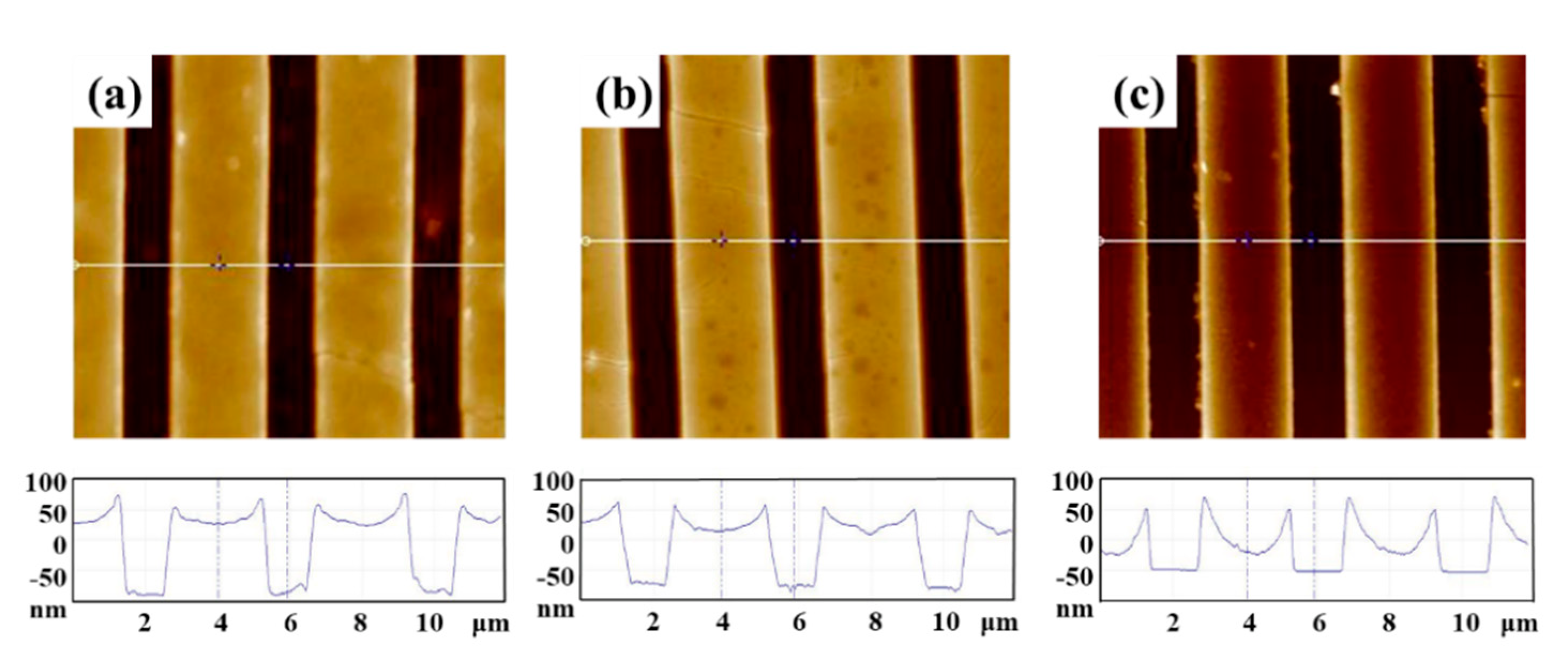
For patterning PMMA/Ti4+, the coating speed of PMMA/Ti4+ film, the contact time between the template and substrate, and the solution concentration were investigated. The AFM image of PDMS template with 1.5 μm line features spaced by 2.5 μm has been introduced in the previous work of our group. Under certain conditions of the PMMA/Ti4+ concentration (1.5%) and the contact time (60 s), the coating speeds of 2000, 4000 and 8000 rpm were adjusted. The cross-section analysis of AFM images in Figure 2 shows that the average height of PMMA/Ti4+ lines increase along with decreasing coating speed. One reason is that less amount of solution is splashed away out of the depressed patterns when the speed is low. The other reason is that the solvent volatilizes slowly under the low coating speed, and then the more solute (PMMA/Ti4+) can move into the PDMS template based on the capillary force. Therefore, the slower the coating speed, the higher the resolution ratio of PMMA/Ti4+ lines. Meanwhile, it is noted that the ‘‘Rabbit ear’’ phenomenon of PMMA/Ti4+ lines is the most obvious with the minimum curvature radius as the highest coating speed of 8000 rpm. This is due to that the compressed degree of air in the template cavity is reduced along with increasing coating−speed, resulting in a smaller curvature radius.
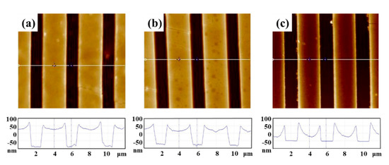
Figure 2.
AFM images of PMMA/Ti4+ lines obtained with different coating speed: (a) 2000 rpm, (b) 4000 rpm and (c) 8000 rpm.
Due to that the glass transition temperature of PMMA is 105 °C, the traditional hot imprinting (HI) needs to keep PMMA as mobile phase to fully move into the template for 20~30 min, which takes a long time and is not conducive to the efficiency of patterning PMMA and its composite [24,25]. In order to explore the patterning efficiency, the influence of the contact time on the PMMA/Ti4+ topography was investigated. Although the coating speed of 2000 rpm, mentioned in the previous paragraph, is most suitable for the sufficient addition of PMMA/Ti4+ into the template, the low coating speed would cause the nonuniform of PMMA/Ti4+ film. Therefore, 4000 rpm is selected as the optimal coating speed with 1.5% PMMA/Ti4+, and different contact time (5 s, 60 s and 180 s) is investigated. With the extension of contact time, there is no significant change of the topography and height of PMMA/Ti4+ lines, as shown in Figure 3. This is because the mechanism of FRTI and traditional HI in the patterning process is different. FRTI is based on the fact that the interface force between the substrate and the patterned material is stronger than that between the template and the patterned material, and the high−efficiency patterning process of PMMA/Ti4+ is completed for 5 s.
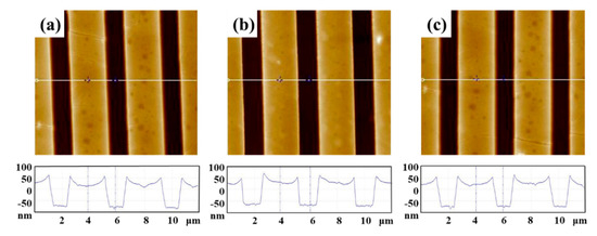
Figure 3.
AFM images of PMMA/Ti4+ lines obtained with different contact time: (a) 5 s, (b) 60 s and (c) 180 s.
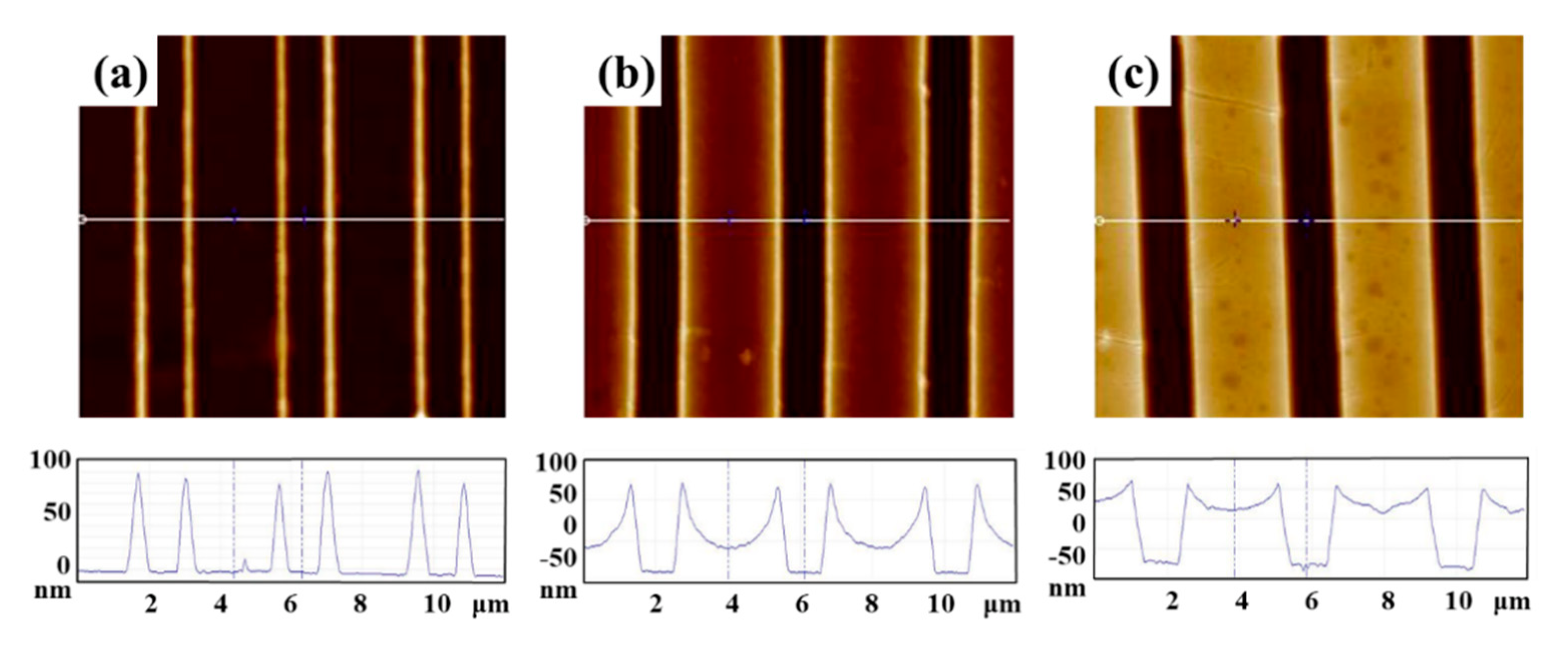
Under the optimization condition of 5 s (contact time) and 4000 rpm (coating speed), the effect of PMMA/Ti4+concentration (0.5%, 1% and 1.5%) on the topography of PMMA/Ti4+ lines was investigated, seeing AFM images and cross−section analysis in Figure 4. The atmosphere outside the PDMS is unsaturated with xylene vapor, leading to a pressure gradient (ΔP) [26] from inside to outside the PDMS, resulting in the solvent gradually evaporating through the PDMS. During the evaporation, the xylene flow brings solute to the side walls of the PDMS, which is the phenomenon of “solvent flow” [19,23]. As solute is less at low concentration, solute can be driven to the side wall edge of PDMS cavity under the action of solvent flow, as shown in Figure 4a. When the concentration is low (the solute is less), the solute can be all driven to the edge of the side wall of the PDMS cavity under the action of the solvent flow, resulting in the higher-resolution lines than the original template, as shown in Figure 4a. When the concentration is high (the solute is more), one part of the solute driven to the edge of the side wall of the PDMS cavity, and the other part of the solute be concentrated in the middle of the PDMS cavity, as shown in Figure 4b,c. Through the above research, the PMMA/Ti4+ lines with different resolution can be fabricated by adjusting the concentration of solution, showing the superiority of this method.
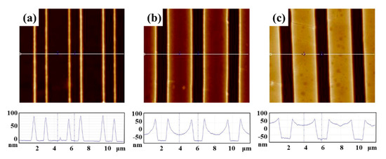
Figure 4.
AFM images of PMMA/Ti4+ lines obtained with different solution concentration: (a) 0.5%, (b) 1% and (c) 1.5%.
From the above discussion, the resolution of PMMA/Ti4+ lines, fabricated under the concentration of 1.5%, the coating speed of 4000 rpm and the contact time of 5 s, is almost the same as that of the original PDMS template, defined as inducer 1. However, the resolution of PMMA/Ti4+ lines, fabricated under the concentration of 0.5%, the coating speed of 4000 rpm and the contact time of 5 s, is higher than that of the original PDMS template, defined as inducer 2. Figure 5a shows the SEM image of TiO2 lines (TiO2 L1) without residual layer, obtained by hydrothermal assembly [27,28,29] for 4 h of inducer 1, which periodicity is in good agreement with that of inducer 1. Figure 5b shows the SEM image of TiO2 lines without residual layer (TiO2 L2), obtained by hydrothermal self-assembly for 4 h of inducer 2, which periodicity is in good agreement with that of inducer 2 and the resolution is much higher than TiO2 L1. Figure 5c shows the SEM image of TiO2 lines without residual layer (TiO2 L3), obtained by hydrothermal self-assembly for 8 h of inducer 2. Due to the overgrowth of TiO2 nano-rods, TiO2 nano-rods on the adjacent lines are connected with each other, resulting in that the resolution of TiO2 L3 is lower than TiO2 L2. The minimum width of TiO2 line is 200 nm in Figure 5b. Meanwhile, the phase composition of the synthesized sample is shown in the XRD diagram of Figure S1, and rutile TiO2 can be observed.
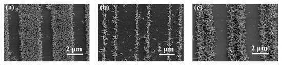
Figure 5.
SEM images of TiO2 lines without residual layer obtained by hydrothermal reaction for (a) 4 h on the inducer 1, for (b) 4 h on the inducer 2 and for (c) 8 h on the inducer 2.
4. Conclusions
The machining of the TiO2 patterns without residual layer was realized by utilizing the difference of interfacial force in the FRTI process. Firstly, the PMMA/Ti4+ film was coated on the PDMS surface by spinning. Secondly, the hydroxyl was modified on the surface of the PMMA/Ti4+ film and the substrate by O2 plasma. Then, the PMMA/Ti4+ film was transferred to the substrate by imprinting. Finally, the PMMA/Ti4+ films were dealt with calcination and hydrothermal reaction to obtain TiO2 patterns without residual layer. Compared with the traditional imprint lithography, this machining method not only avoids high temperature and high pressure, but also solves the problem for residual layer of TiO2 patterns. This method provides a new idea to pattern metal oxide without residual layer, which is potentially applied to the gas sensor, the optical detector and the light emitting diode.
Supplementary Materials
The following are available online at https://www.mdpi.com/article/10.3390/app112110097/s1, Figure S1: AFM image of original FRTI stamp.
Author Contributions
Conceptualization, Y.L.; methodology, G.S. and Z.Z.; validation, Y.L.; formal analysis, Z.Z. and Y.L.; investigation, Z.Z. and Y.L.; resources, G.S. and Y.L.; data curation, Y.L.; writing—original draft preparation, Z.Z.; writing—review and editing, Y.L., L.M.U. and F.I.T.P.; funding acquisition, G.S. and Y.L. All authors have read and agreed to the published version of the manuscript.
Funding
This work was supported by National Natural Science Foundation of China (21671081), Fok Ying Tong Education Foundation (171039) and MOE & SAFEA for the 111 Project (B13025).
Institutional Review Board Statement
Not applicable.
Informed Consent Statement
Not applicable.
Data Availability Statement
Not applicable.
Acknowledgments
The support from Central Laboratory, School of Chemical and Material Engineering, Jiangnan University, is appreciated.
Conflicts of Interest
The authors declare no conflict of interest.
References
- Liu, L.; He, N.; Wu, T.; Hu, P.; Tong, G. Co/C/Fe/C hierarchical flowers with strawberry-like surface as surface plasmon for enhanced permittivity, permeability, and microwave absorption properties. Chem. Eng. J. 2019, 355, 103–108. [Google Scholar] [CrossRef]
- Zhan, D.; Han, L.; Zhang, J.; He, Q.; Tian, Z.; Tian, Z. Electrochemical micro/nano-machining: Principles and practices. Chem. Soc. Rev. 2017, 46, 1526–1544. [Google Scholar] [CrossRef]
- Chen, Y.; Wang, H.; Yao, Q.; Fan, B.; Wang, C.; Xiong, Y.; Jin, C.; Sun, Q. Biomimetic taro leaf-like films decorated on wood surfaces using soft lithography for superparamagnetic and superhydrophobic performance. J. Mater. Sci. 2017, 52, 7428–7438. [Google Scholar] [CrossRef]
- Heinz, O.; Aghajani, M.; Greenberg, A.R.; Ding, Y. Surface-patterning of polymeric membranes: Fabrication and performance. Curr. Opin. Chem. Eng. 2018, 20, 1–12. [Google Scholar] [CrossRef]
- Hirota, K.; Hara, S.; Wada, H.; Shimojima, A.; Kuroda, K. Fabrication of uniaxially aligned silica nanogrooves with sub-5 nm periodicity on centimeter-scale Si substrate using poly(dimethylsiloxane) stamps. ACS Nano 2019, 13, 2795–2803. [Google Scholar] [CrossRef]
- Yang, B.; Cai, F.; Huang, S.; Yu, H. Athermal and soft multi-nanopatterning of azopolymers: Phototunable mechanical properties. Angew. Chem. Int. Ed. 2020, 59, 4035–4042. [Google Scholar] [CrossRef] [PubMed]
- Mathies, F.; Brenner, P.; Hernandez-Sosa, G.; Howard, I.A.; Paetzold, U.W.; Lemmer, U. Inkjet-printed perovskite distributed feedback lasers. Opt. Express 2018, 26, A144–A152. [Google Scholar] [CrossRef] [PubMed]
- Jin, X.; Zhu, Q.; Feng, L.; Li, X.; Zhu, H.; Miao, H.; Zeng, Z.; Wang, Y.; Li, Y.; Wang, L.; et al. Light-trapping SERS substrate with regular bioinspired arrays for detecting trace dyes. ACS Appl. Mater. Interfaces 2021, 13, 11535–11542. [Google Scholar] [CrossRef]
- Kim, E.; Xia, Y.; Whitesides, G.M. Micromolding in capillaries: applications in materials science. J. Am. Chem. Soc. 1996, 118, 5722–5731. [Google Scholar] [CrossRef]
- Shi, G.; Li, L.; Liu, L.; Xu, D.; Lu, N.; Hao, J.; Huang, C.; Chi, L. Conducting polymer nanowires fabricated by edge effect of NIL. J. Mater. Chem. 2012, 22, 12096–12099. [Google Scholar] [CrossRef]
- Shi, G.; Lu, N.; Xu, H.; Wang, Y.; Shi, S.; Li, H.; Li, Y.; Chi, L. Fabrication of hierarchical structures by unconventional two-step imprinting. J. Colloid Interface Sci. 2012, 368, 655–659. [Google Scholar] [CrossRef] [PubMed]
- Suh, K.Y.; Kim, Y.S.; Lee, H.H. Capillary force lithography. Adv. Mater. 2001, 13, 1386–1389. [Google Scholar] [CrossRef]
- Suh, K.Y.; Park, M.C.; Kim, P. Capillary force lithography: A versatile tool for structured biomaterials interface towards cell and tissue engineering. Adv. Funct. Mater. 2009, 19, 2699–2712. [Google Scholar] [CrossRef]
- McLellan, J.M.; Geissler, M.; Xia, Y. Edge spreading lithography and its application to the fabrication of mesoscopic gold and silver rings. J. Am. Chem. Soc. 2004, 126, 10830–10831. [Google Scholar] [CrossRef] [PubMed]
- Cavallini, M.; Albonetti, C.; Biscarini, F. Nanopatterning soluble multifunctional materials by unconventional wet lithography. Adv. Mater. 2009, 21, 1043–1053. [Google Scholar] [CrossRef]
- Xue, L.; Han, Y. Pattern formation by dewetting of polymer thin film. Prog. Polym. Sci. 2011, 36, 269–293. [Google Scholar] [CrossRef]
- Janczarek, M.; Kowalska, E. On the origin of enhanced photocatalytic activity of copper-modified Titania in the oxidative reaction systems. Catalysts 2017, 7, 317. [Google Scholar] [CrossRef] [Green Version]
- Kubiak, A.; Siwinska-Ciesielczyk, K.; Jesionowski, T. Titania-Based Hybrid Materials with ZnO, ZrO2 and MoS2: A Review. Materials 2018, 11, 2295. [Google Scholar] [CrossRef] [Green Version]
- Shi, G.; Lu, N.; Gao, L.; Xu, H.; Yang, B.; Li, Y.; Wu, Y.; Chi, L. Fabrication of TiO2 arrays using solvent-assisted soft lithography. Langmuir 2009, 25, 9639–9643. [Google Scholar] [CrossRef]
- Liu, B.; Aydil, E.S. Growth of oriented single-crystalline rutile TiO2 nanorods on transparent conducting substrates for dye-sensitized solar cells. J. Am. Chem. Soc. 2009, 131, 3985–3990. [Google Scholar] [CrossRef]
- Shi, G.; Li, X.; Sang, X.; Wang, L.; Bai, H.; Yang, J.; Ni, C.; Li, Y. Patterning thermoplastic polymers by fast room temperature imprinting. J. Mater. Sci. 2018, 53, 5429–5435. [Google Scholar] [CrossRef]
- Song, L.; Gutmann, J.S.; Frielinghaus, H.; Müller-Buschbaum, P. Deformation of mesoporous titania nanostructures in contact with D2O vapor. Small 2018, 14, 1801461. [Google Scholar] [CrossRef] [Green Version]
- Sun, F.; Yu, J.C.; Wang, X. Construction of Size-Controllable Hierarchical Nanoporous TiO2 Ring Arrays and Their Modifications. Chem. Mater. 2006, 18, 3774–3779. [Google Scholar] [CrossRef]
- Horvath, B.; Krivova, B.; Bolat, S.; Schift, H. Fabrication of Large Area Sub-200 nm Conducting Electrode Arrays by Self-Confinement of Spincoated Metal Nanoparticle Inks. Adv. Mater. Technol. 2019, 4, 1800652. [Google Scholar] [CrossRef]
- Lane, A.P.; Yang, X.; Maher, M.J.; Blachut, G.; Asano, Y.; Someya, Y.; Mallavarapu, A.; Sirard, S.M.; Ellison, C.J.; Willson, C.G. Directed self-assembly and pattern transfer of five nanometer block copolymer lamellae. ACS Nano 2017, 11, 7656–7665. [Google Scholar] [CrossRef]
- Dimitrov, A.S.; Nagayama, K. Continuous Convective Assembling of Fine Particles into Two-Dimensional Arrays on Solid Surfaces. Langmuir 1996, 12, 1303–1311. [Google Scholar] [CrossRef]
- Shi, G.; Li, J.; Li, Y.; Zhang, L.; Ni, C.; Chi, L. Fabrication of 3D biomimetic composite coating with broadband antireflection, super-hydrophilicity and double p-n hetero-junctions. Nano Res. 2017, 10, 2377–2385. [Google Scholar] [CrossRef]
- Shi, G.; Chen, J.; Wang, L.; Wang, D.; Yang, J.; Li, Y.; Zhang, L.; Ni, C.; Chi, L. Titanium oxide/silicon moth-eye structures with antireflection, p–n heterojunctions, and superhydrophilicity. Langmuir 2016, 32, 10719–10724. [Google Scholar] [CrossRef]
- Shi, G.; Li, J.; Sang, X.; Wang, L.; Ni, C.; Li, Y. Micro-nano fabrication of hierarchical PPy/TiO2/Si by continuous self-assembly technology. Mater. Manuf. Process. 2018, 33, 378–382. [Google Scholar] [CrossRef]


Publisher’s Note: MDPI stays neutral with regard to jurisdictional claims in published maps and institutional affiliations. |
© 2021 by the authors. Licensee MDPI, Basel, Switzerland. This article is an open access article distributed under the terms and conditions of the Creative Commons Attribution (CC BY) license (https://creativecommons.org/licenses/by/4.0/).