
Tunable Mixed-Mode Voltage Differencing Buffered Amplifier-Based Universal Filter with Independently High-Q Factor Controllability

 ,
,  ,
,  and
and
Abstract
1. Introduction
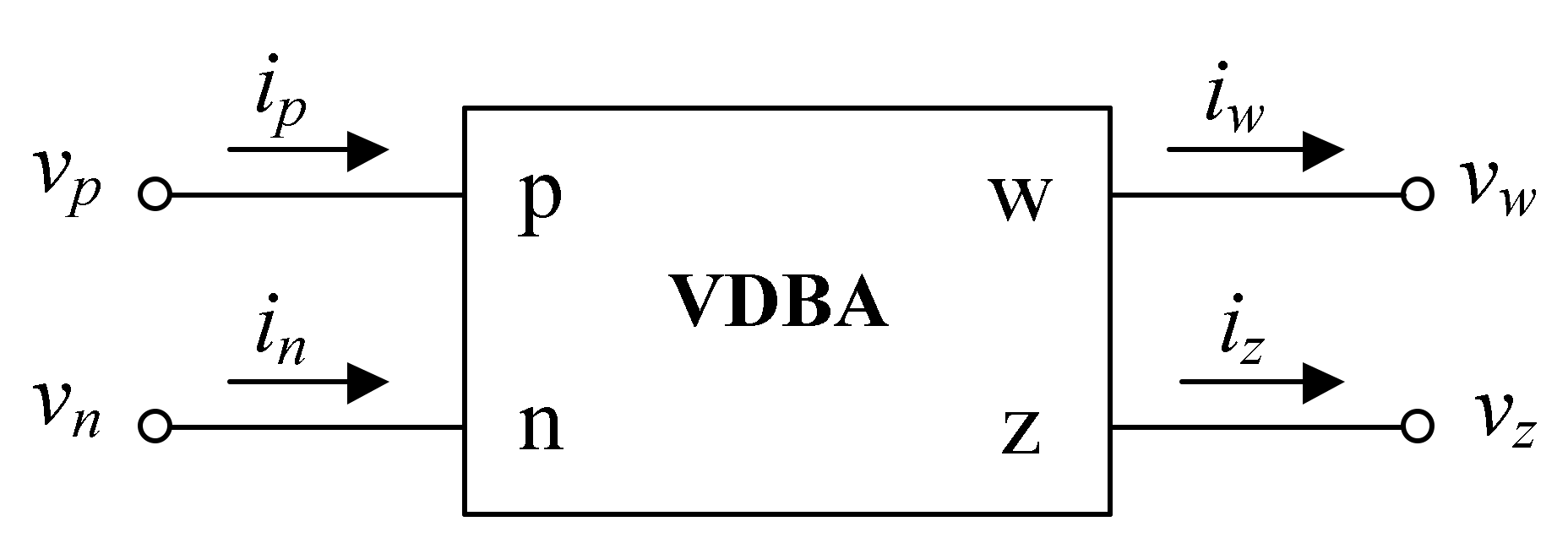
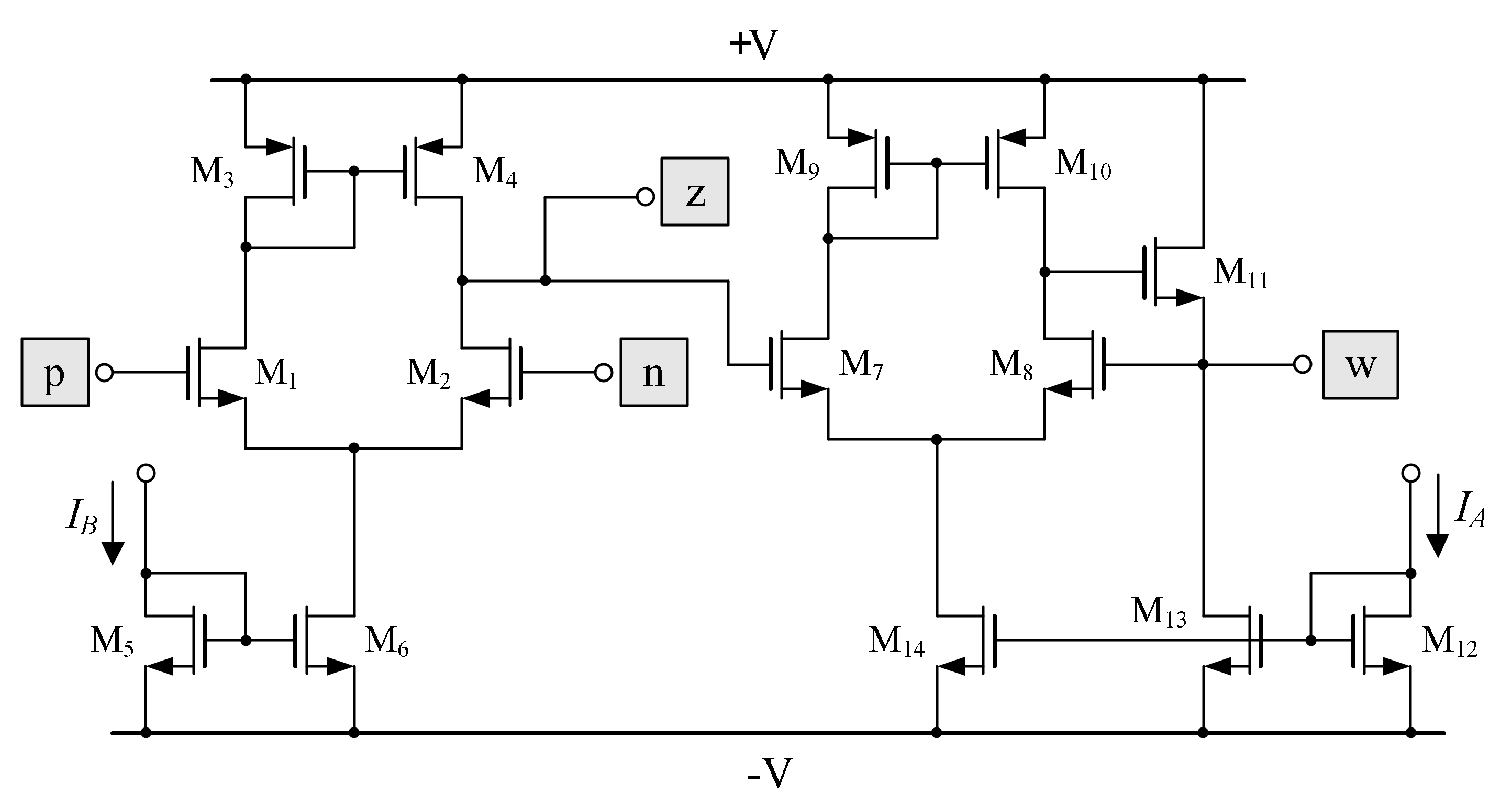
2. VDBA Description
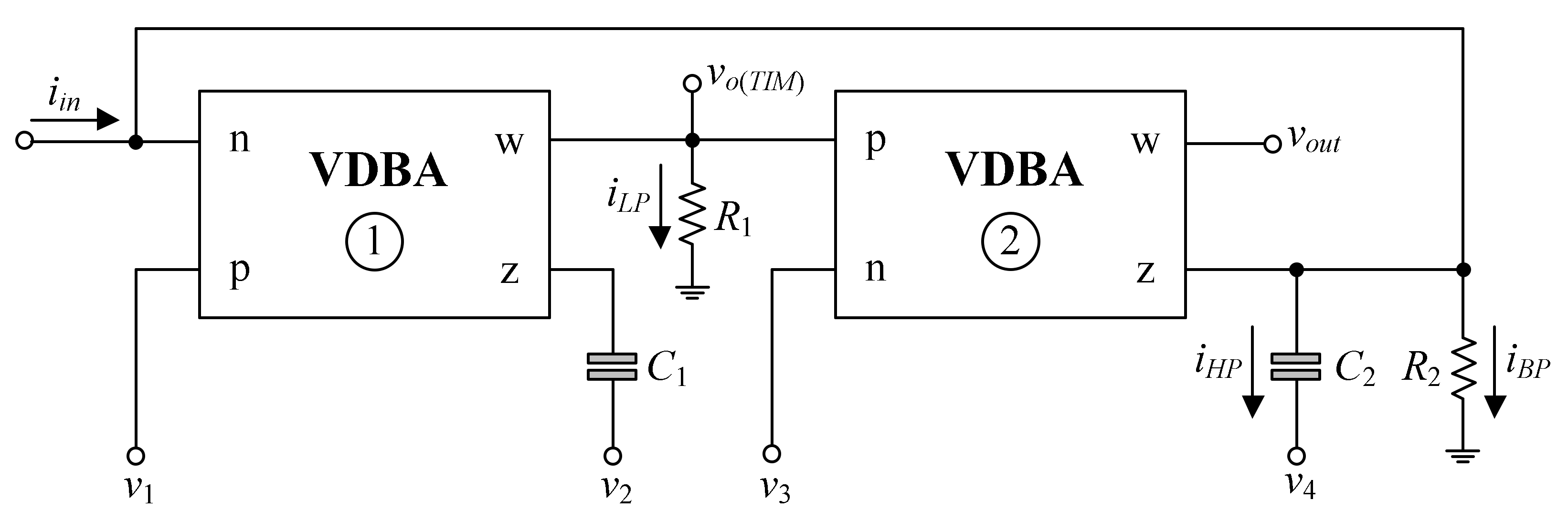
3. Proposed Mixed-Mode Universal Biquad Filter
- ⮚
- For VM operation: Assuming ideal VDBA (i.e., α =β = 1) and setting iin = 0, the general voltage biquadratic transfer functions of this MISO filter can be obtained as follows.
- With vin = v1 (input voltage) and v2 = v3 = v4 = 0 (grounded), then the LP response is realized as:
- With vin = v2, v1 = v3 = v4 = 0, and gm2 = 1/R2, then the BP response is realized as:
- With vin = v4, and v1 = v2 = v3 = 0, then the HP response is realized as:
- With vin = v1 = v4, and v2 = v3 = 0, then the BS response is realized as:
- With vin = v1 = v3 = v4, v2 = 0, and gm2 = 1/R2, then the AP response is realized as:whereUnder appropriate conditions, the proposed circuit realizes all five generic biquadratic filter responses at vout, which are taken from the w-terminal of VDBA2. Thus, the voltage output of the circuit has a very low output impedance, which is suitable for VM cascadability. Moreover, in this MISO configuration, there is no requirement for negative and double input voltage signals to realize the desired filter responses.
- ⮚
- For CM operation: If v1 = v2 = v3 = v4 = 0 (grounded), the CM biquad transfer functions for this SIMO filter, attained from the circuit analysis of Figure 3, are given byandwhere H0 is the passband gain equal to 1/gm2R1. Additionally, for R1 = 1/gm2, the BS current response can be realized by connecting the appropriate output currents as iBS = iHP – iLP. In the same way, the AP response can also be obtained by the interconnection of LP, BP, and HP responses as iAP = iHP – iBP – iLP.
- ⮚
- For TAM operation: With vin = v3 and v1 = v2 = v4 = 0, then we obtain the TAM filter functions as follows:andEquations (12)–(16) represent the TAM filter functions of the LP, BP, HP, BS, and AP responses with controllable passband gains, respectively. Gain constants can be defined as H1 = 1/R1 and H2 = gm2. It should also be noted from Equations (15) and (16) that a simple component matching condition (R1 = 1/gm2) is required in the case of BS and AP filter realizations.
- ⮚
- For TIM operation: With all input voltages kept grounded (v1 = v2 = v3 = v4 = 0), the configuration in Figure 3 now works in TIM. For this operation, the circuit will realize only two LP and BP biquad filter functions without the requirement of any component matching constraints. The TIM transfer functions related to the outputs vout and vo(TIM) of the circuit are given byandwhere H3 = R2.
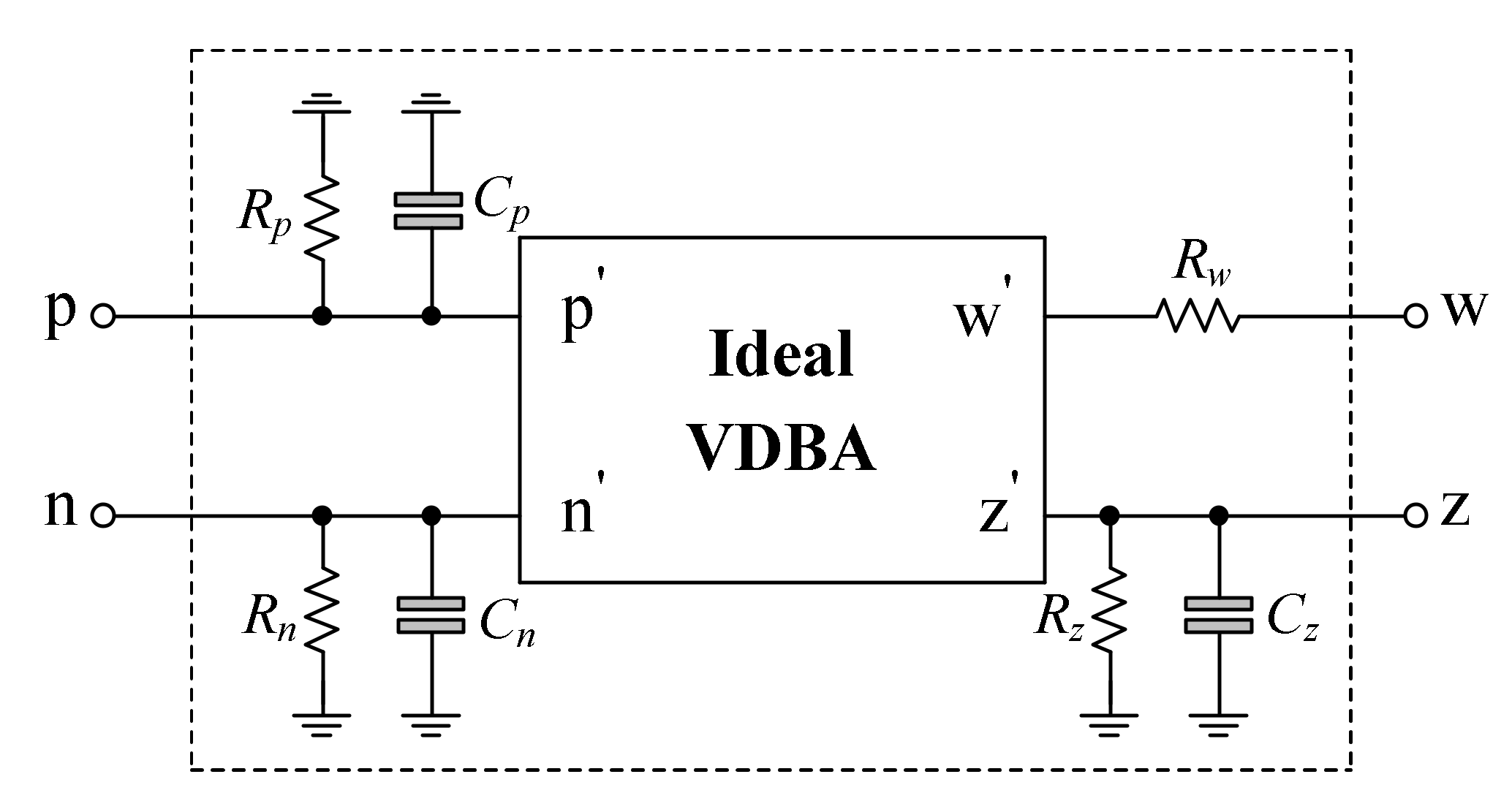
4. Analysis of the Non-Ideal Gain Effect and Sensitivity Performance
5. Analysis of the Parasitic Impedance Effect
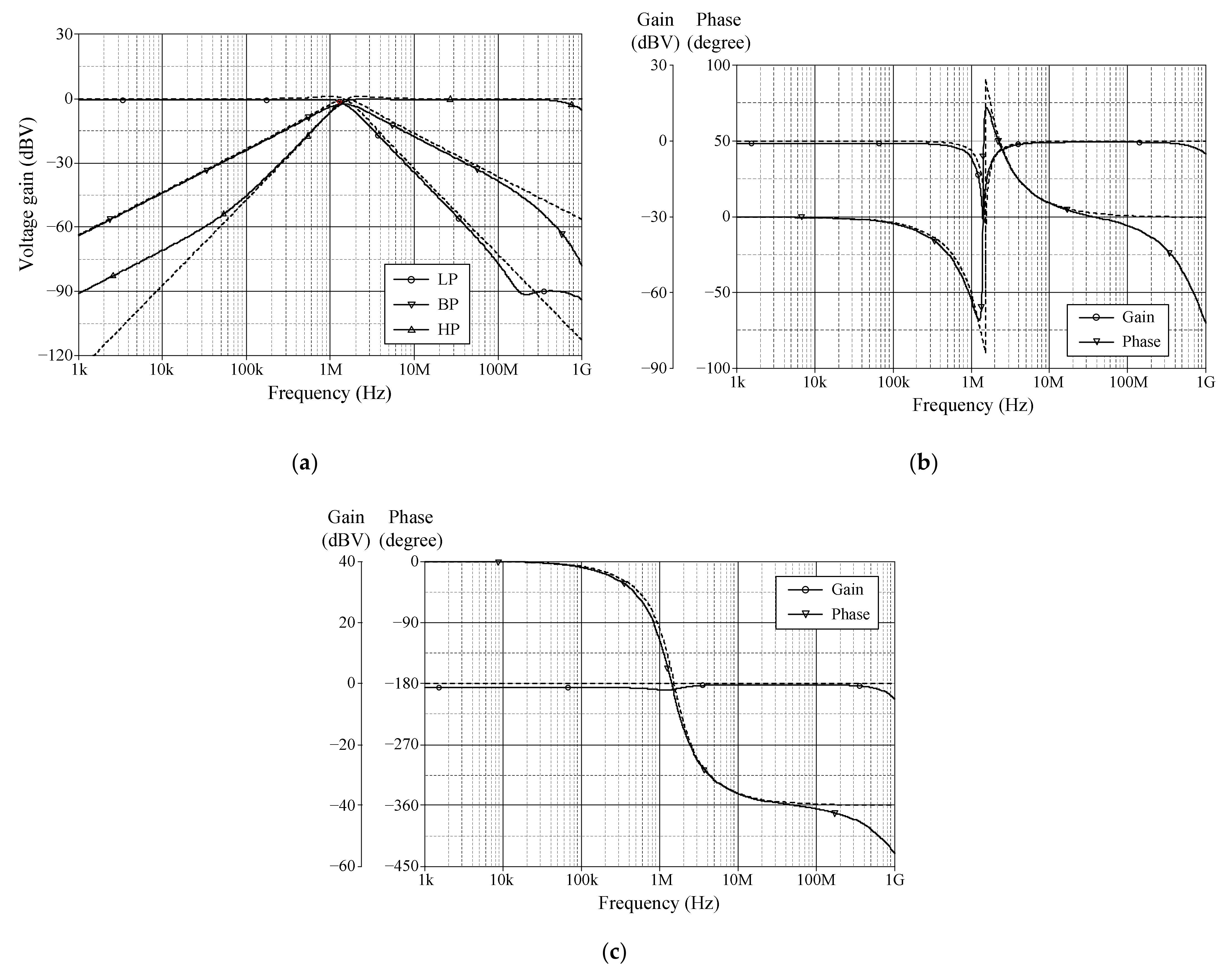
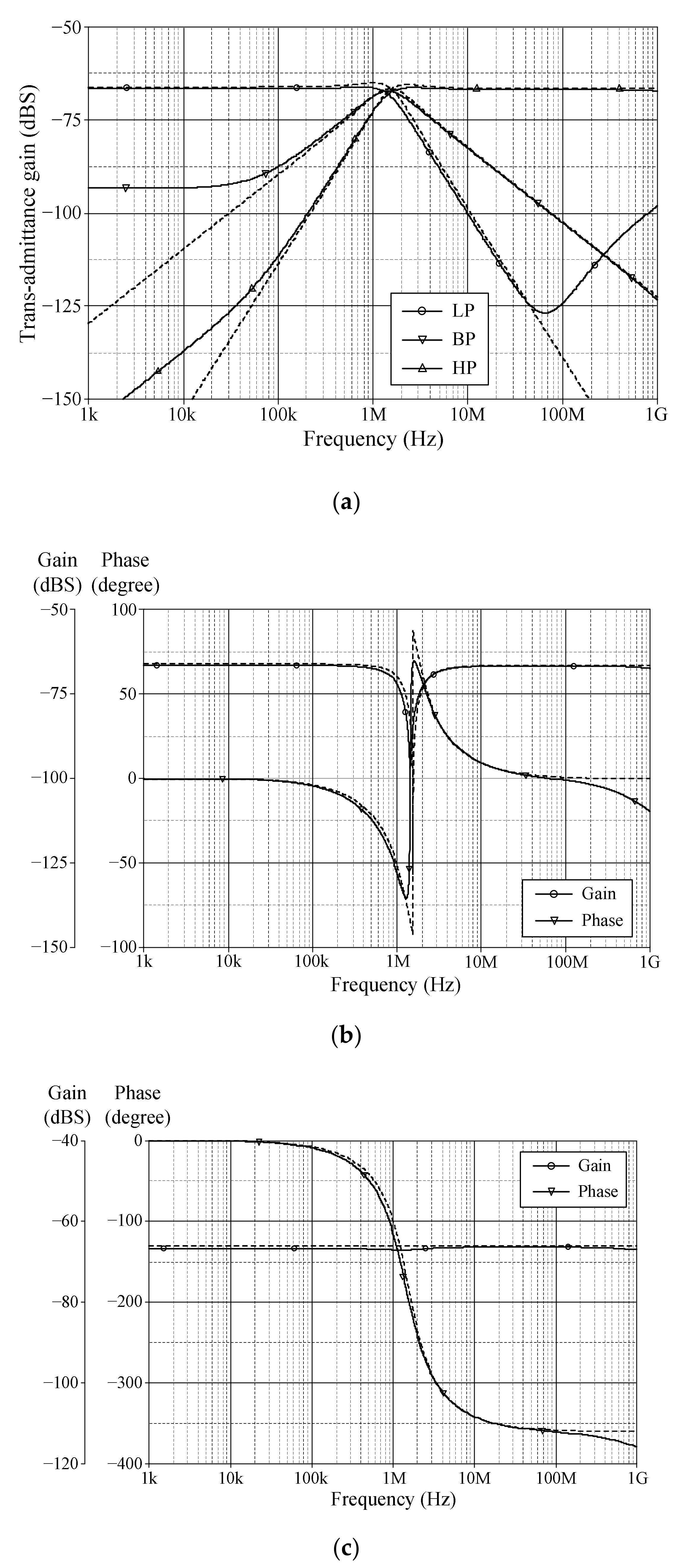
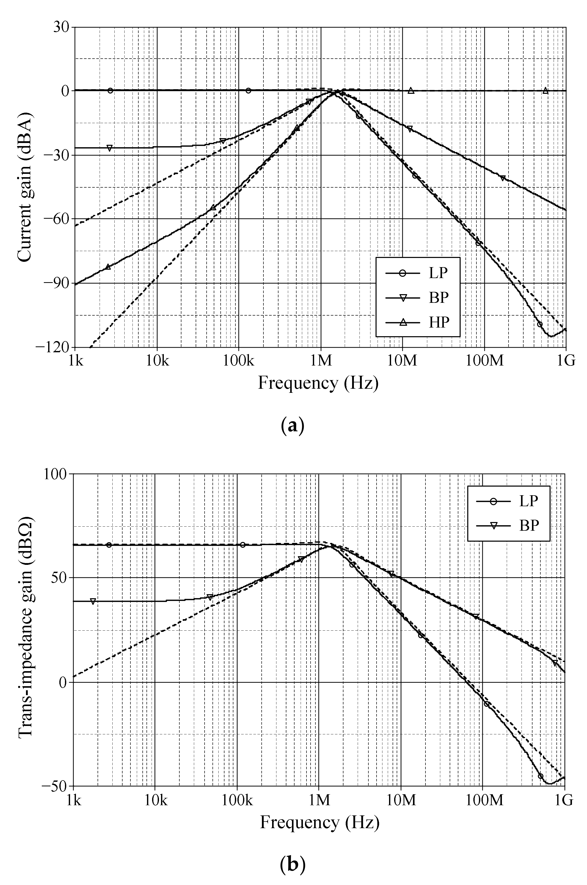
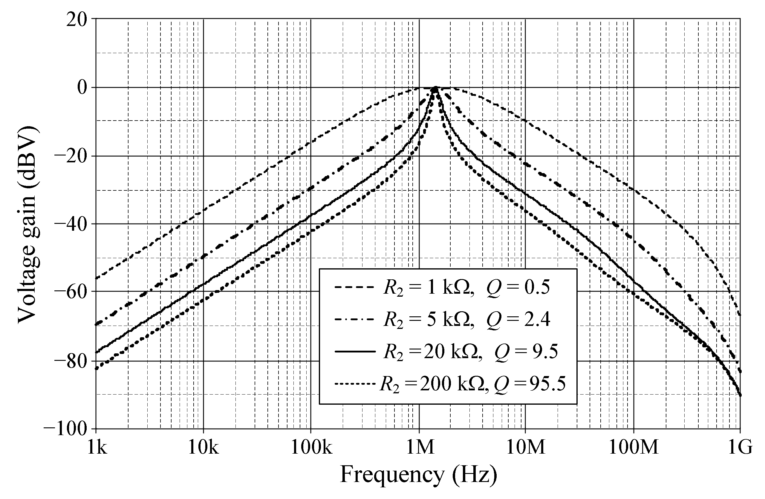
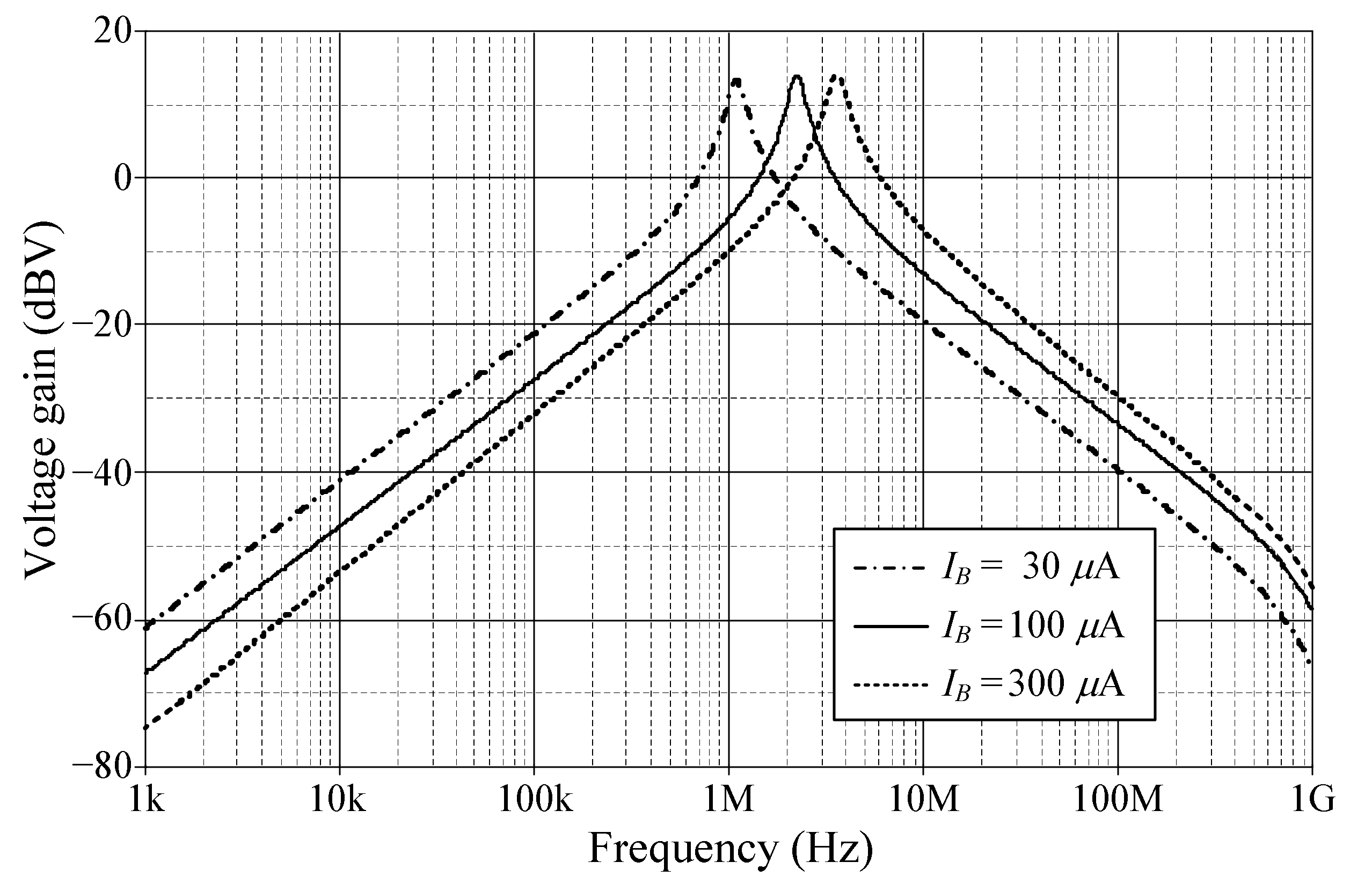
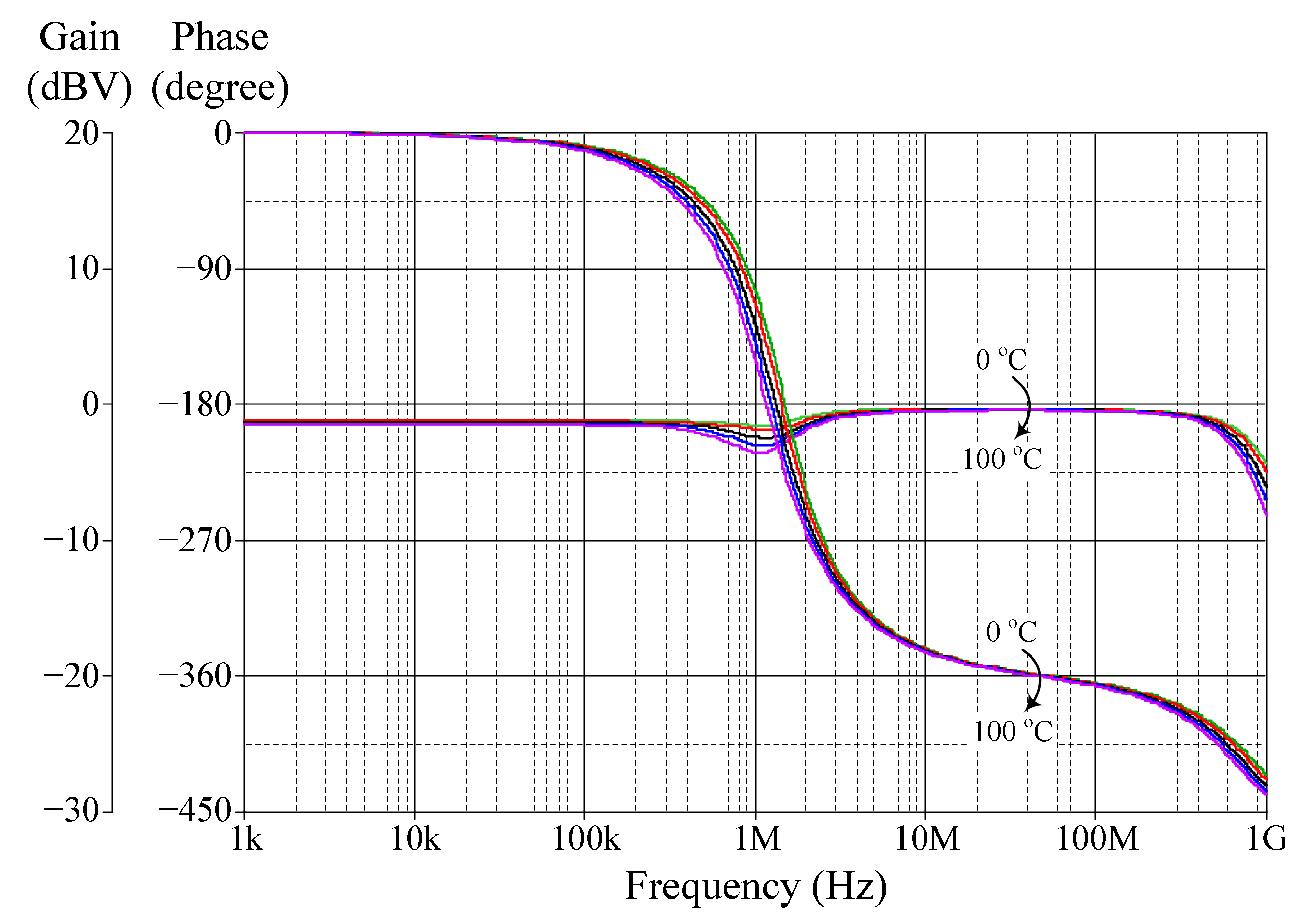
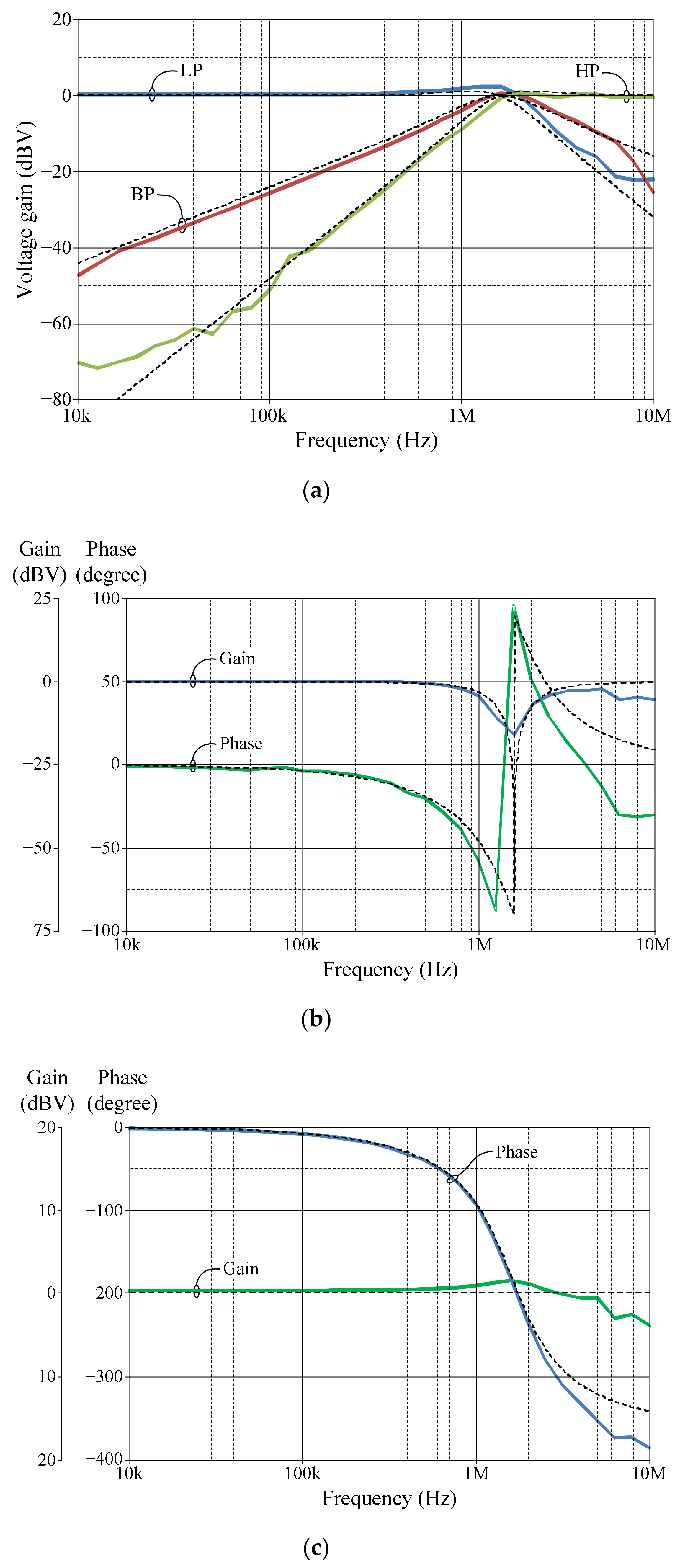
6. Simulation Results
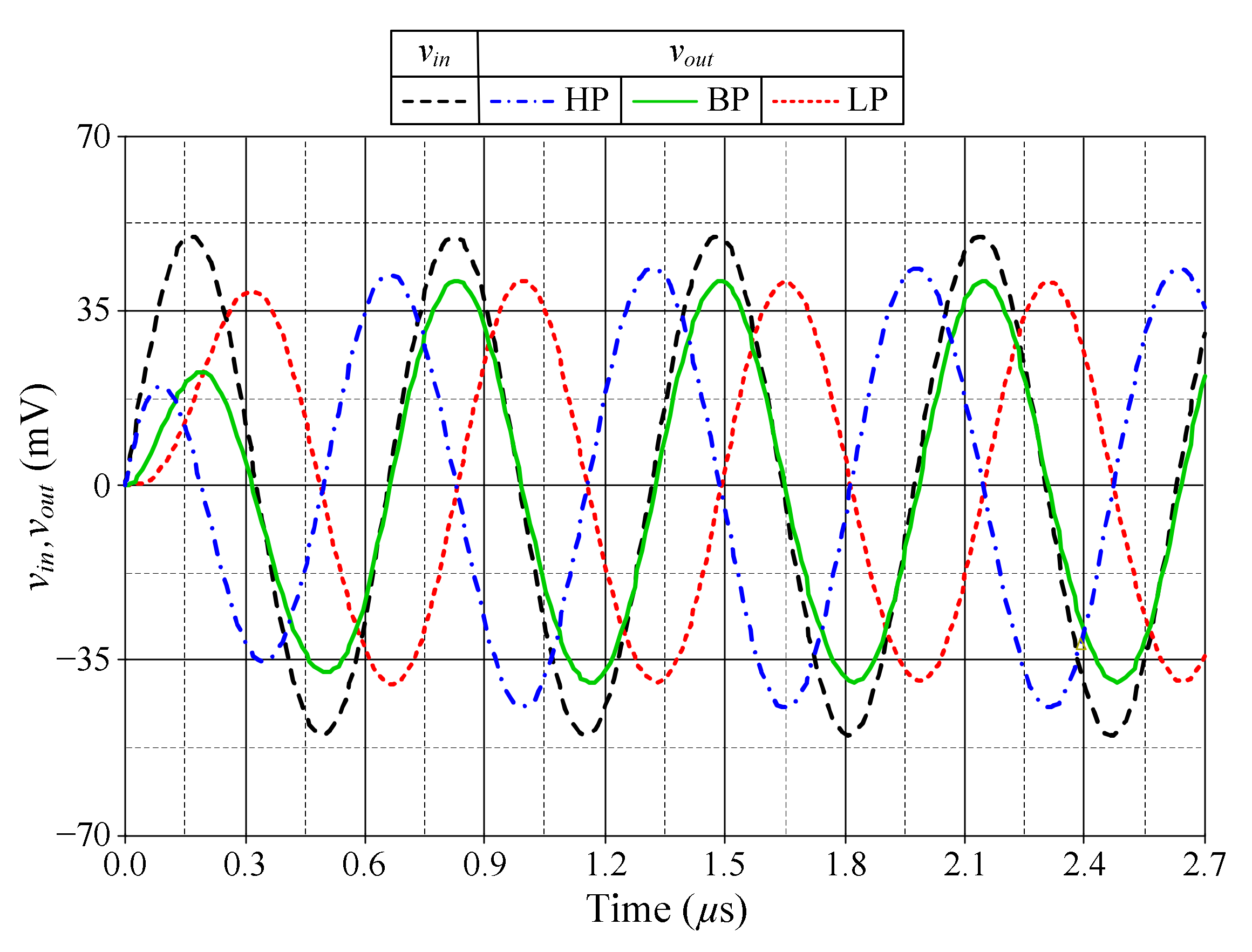
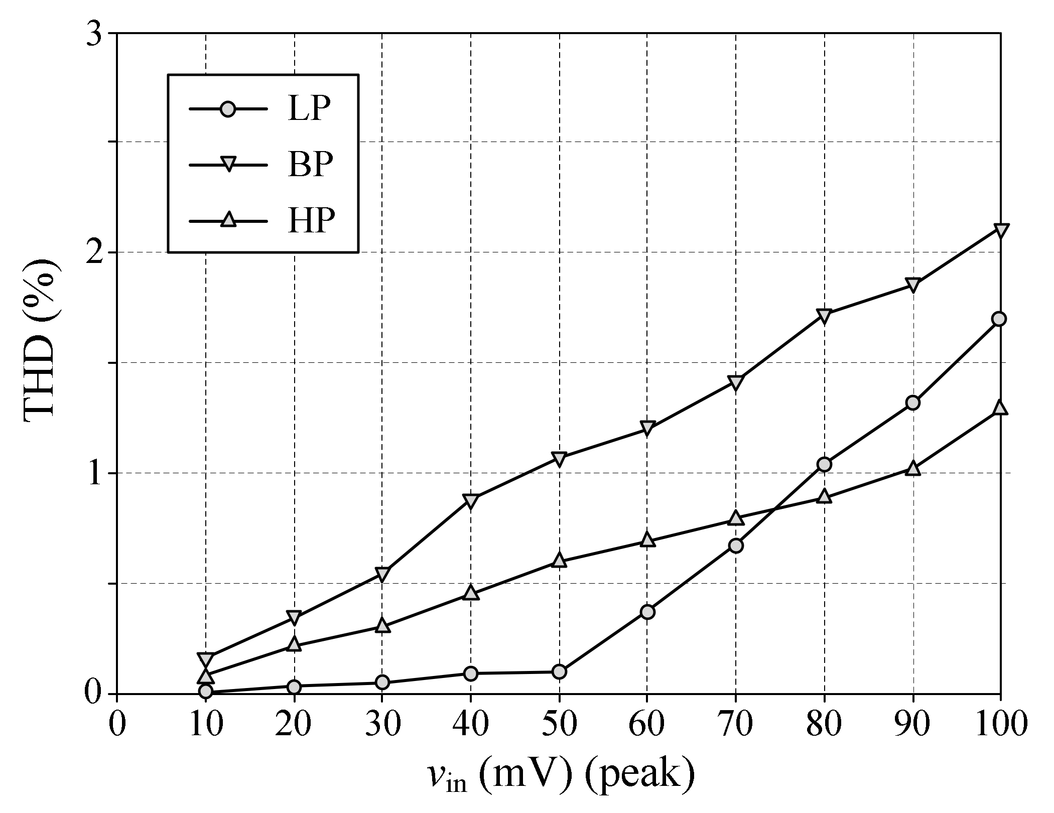
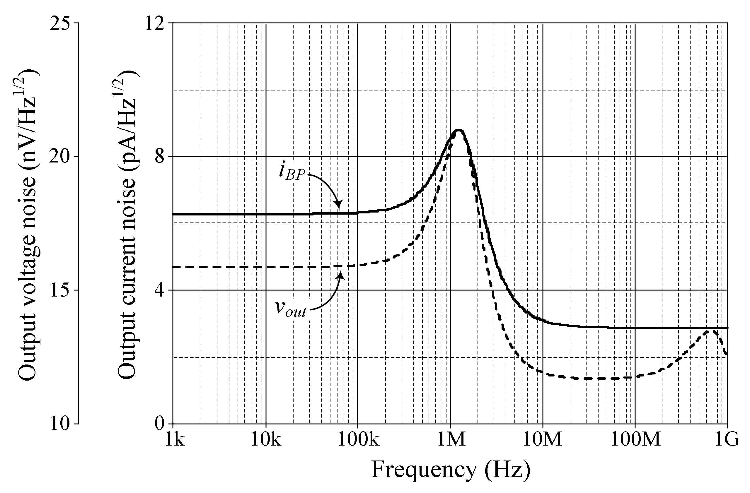
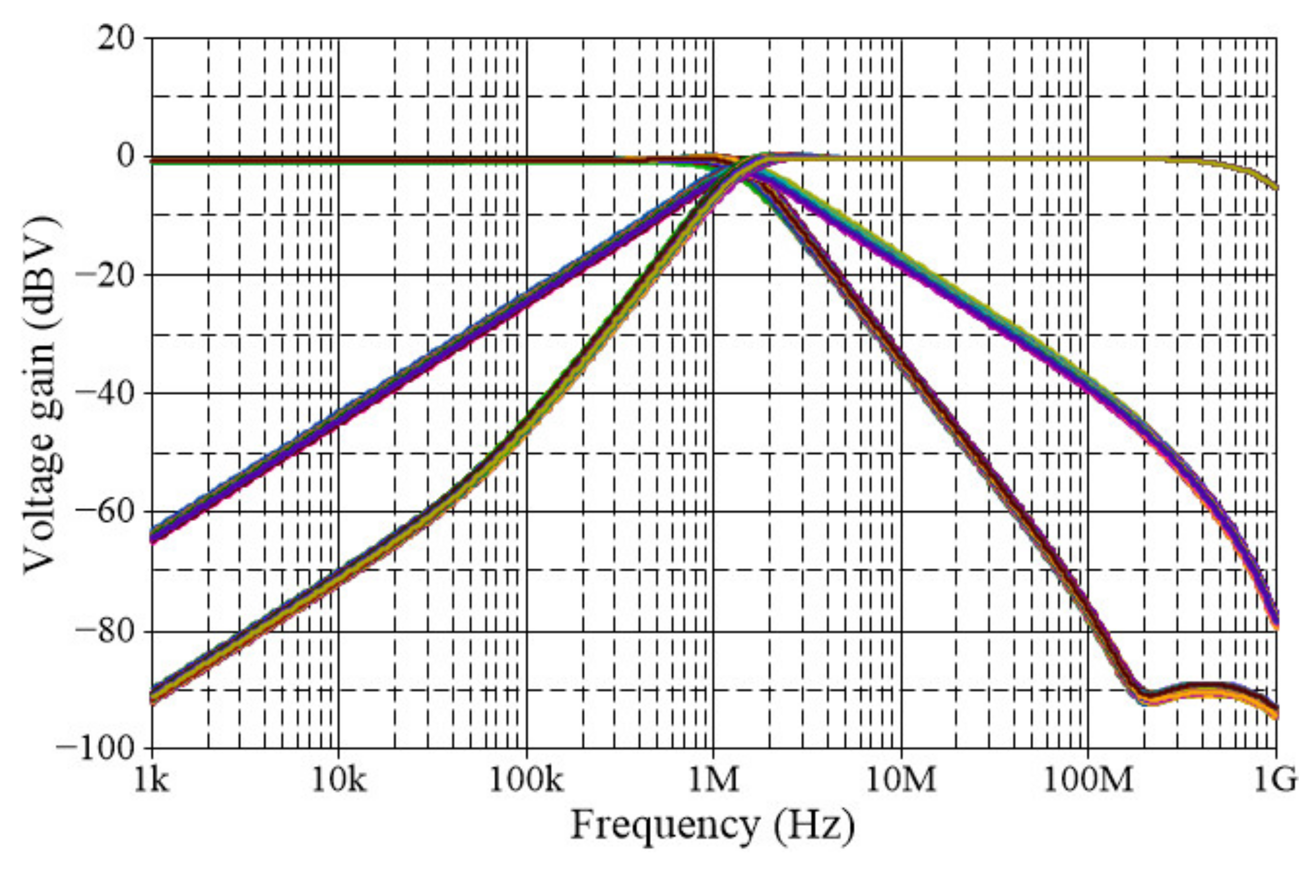
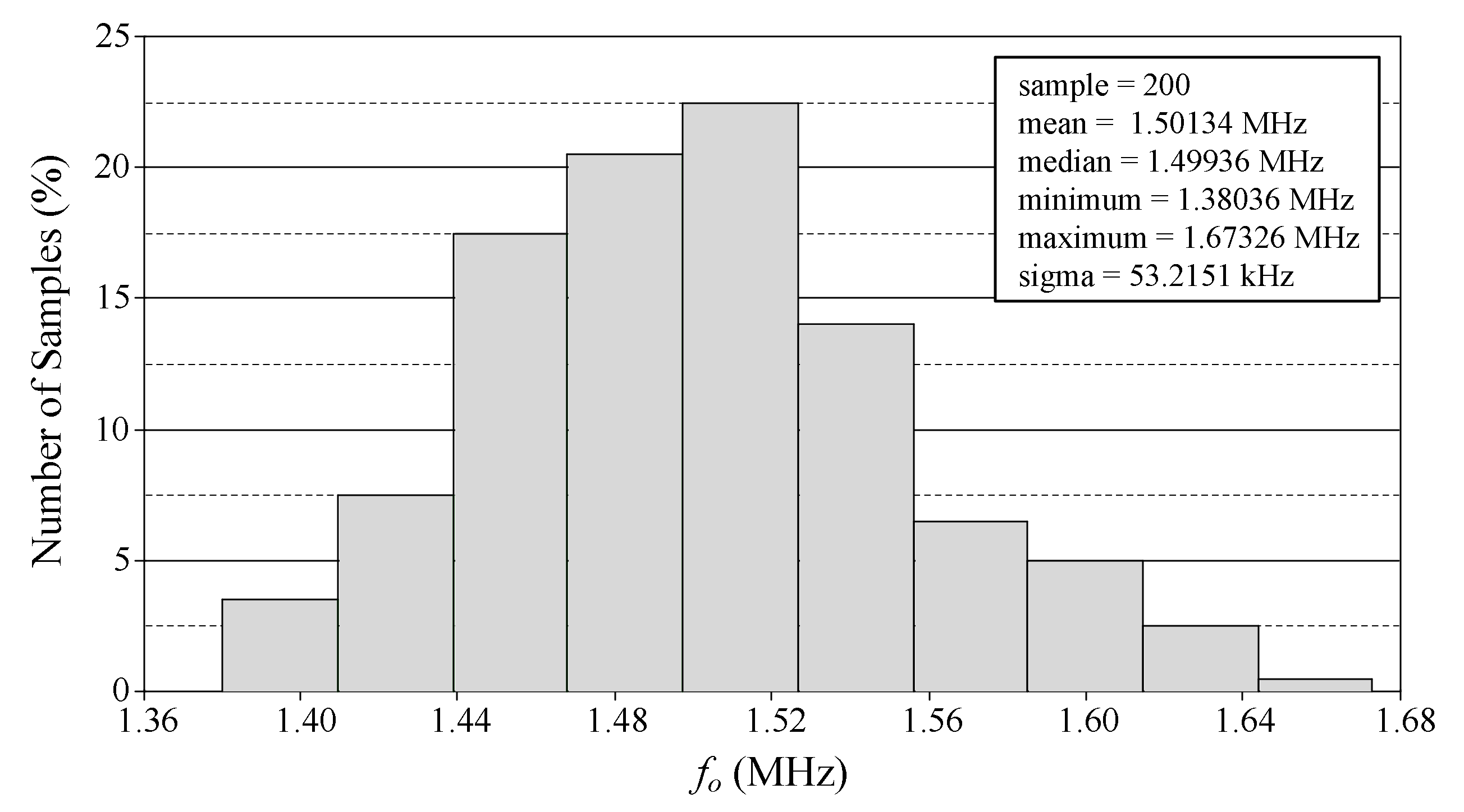
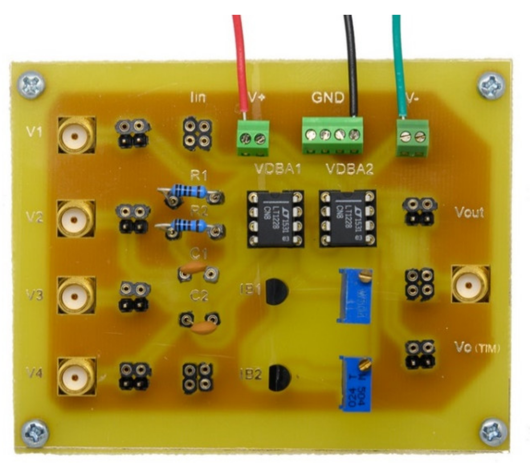
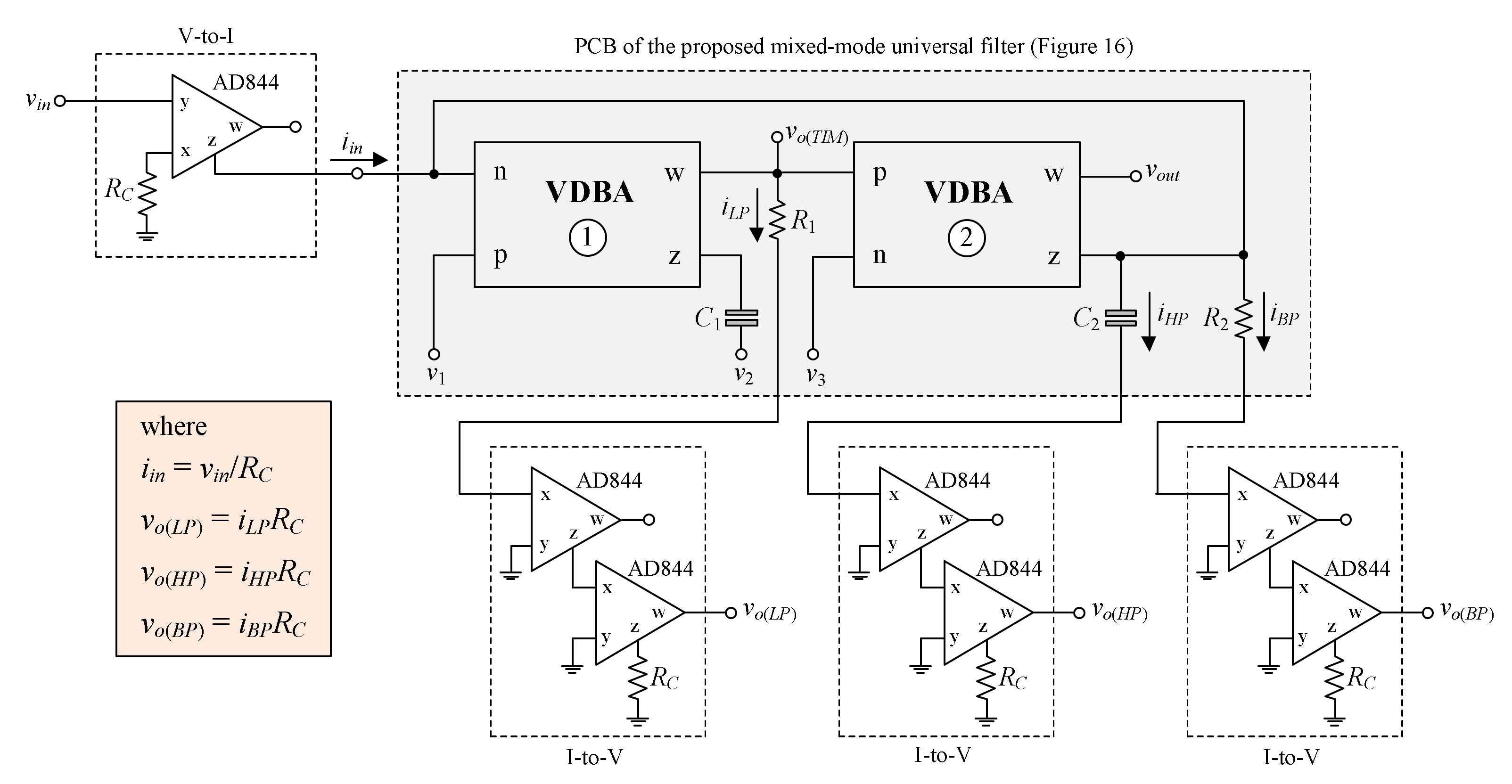
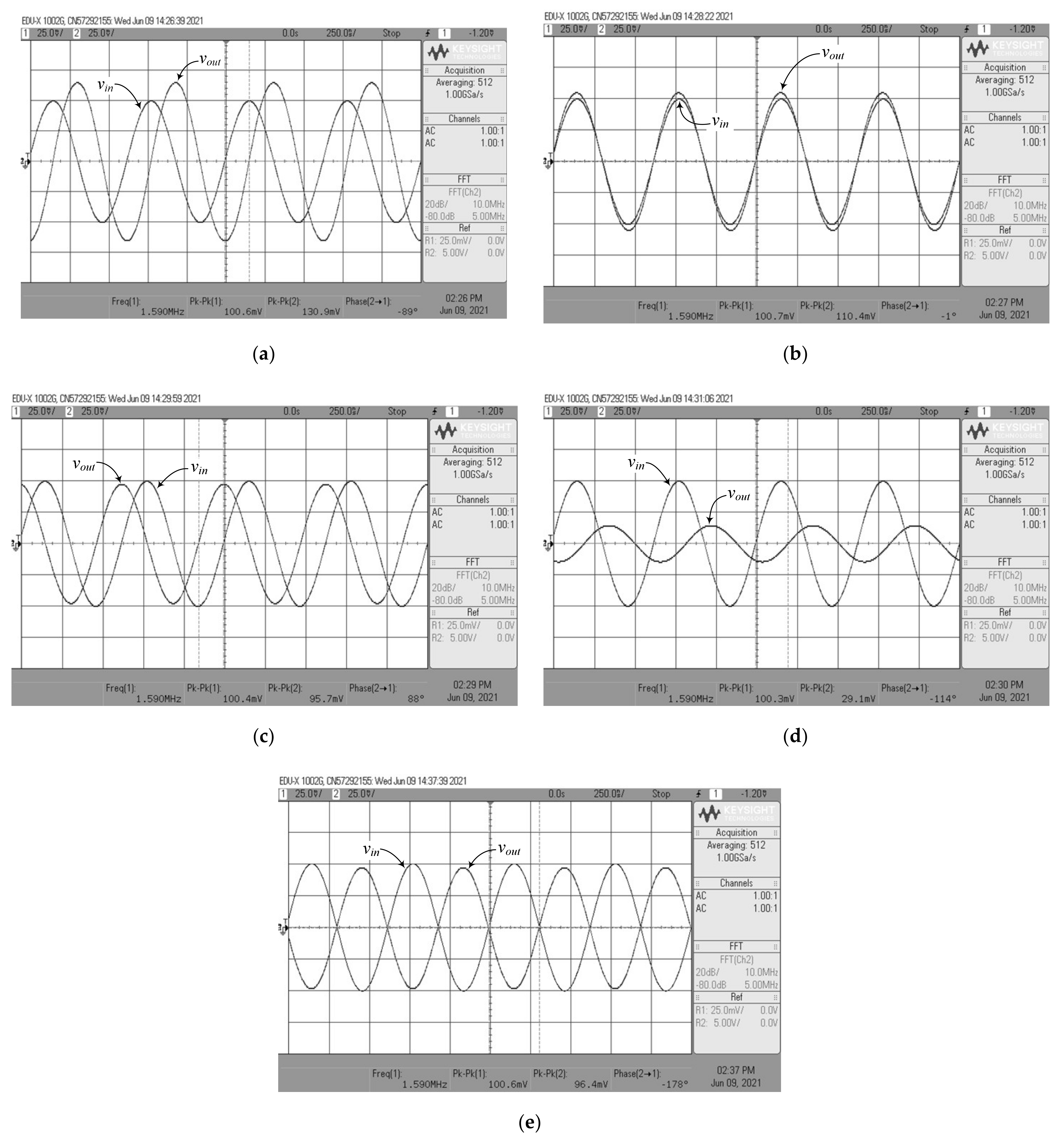
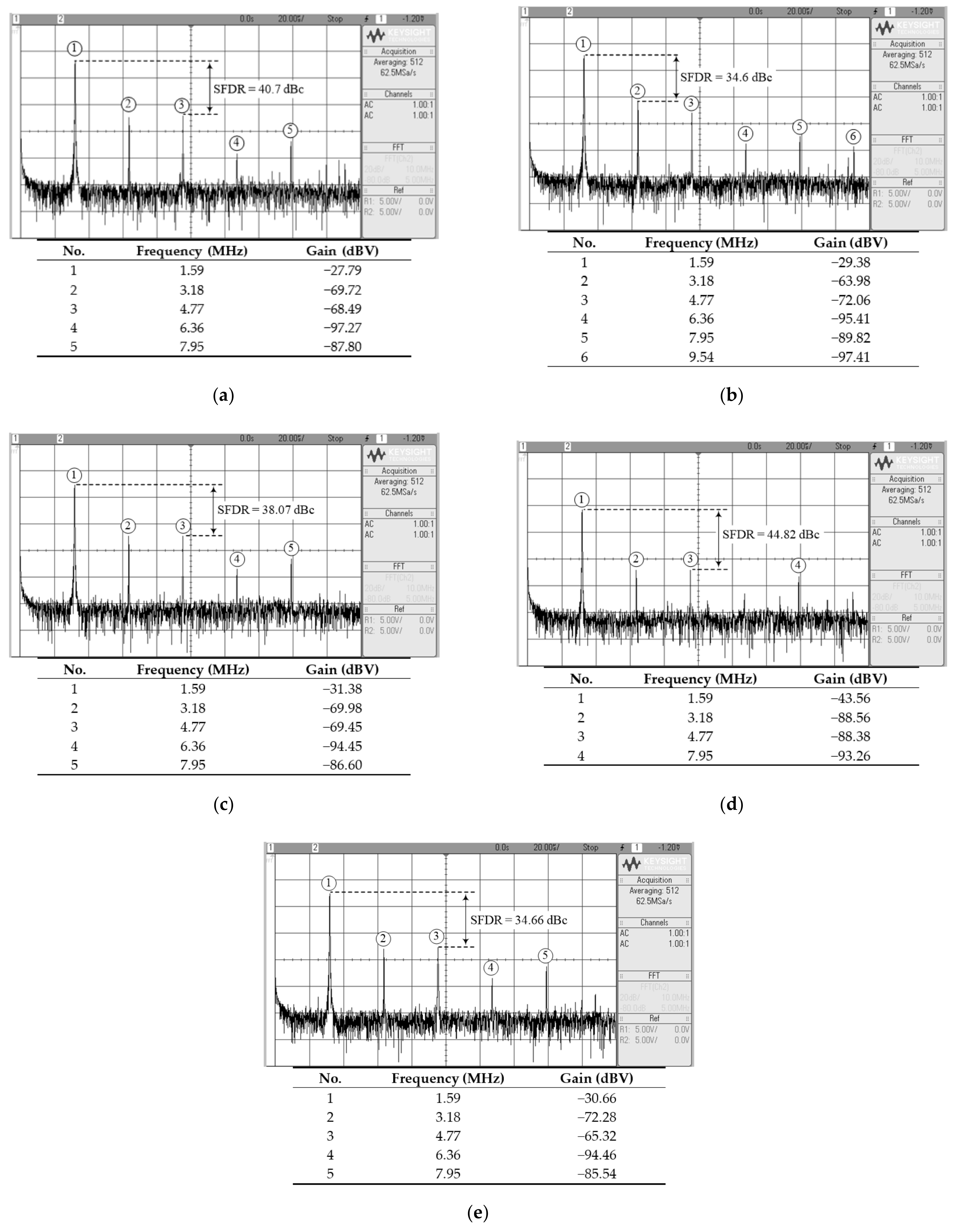
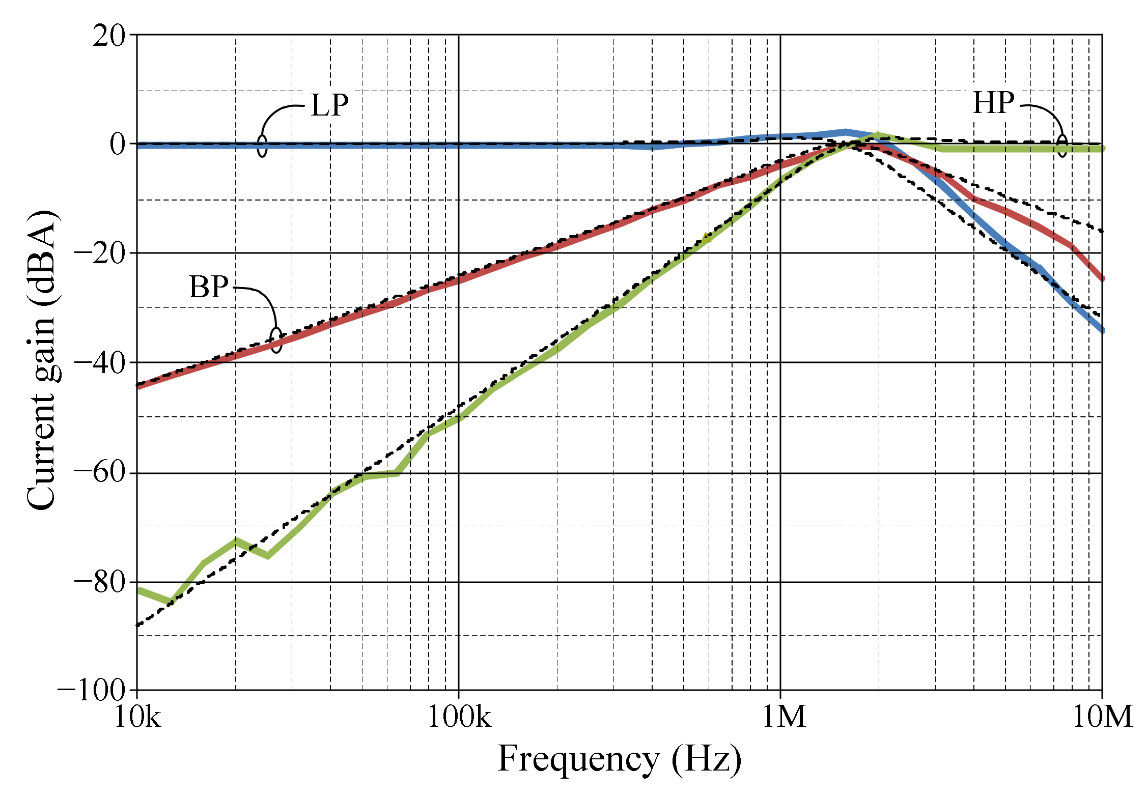
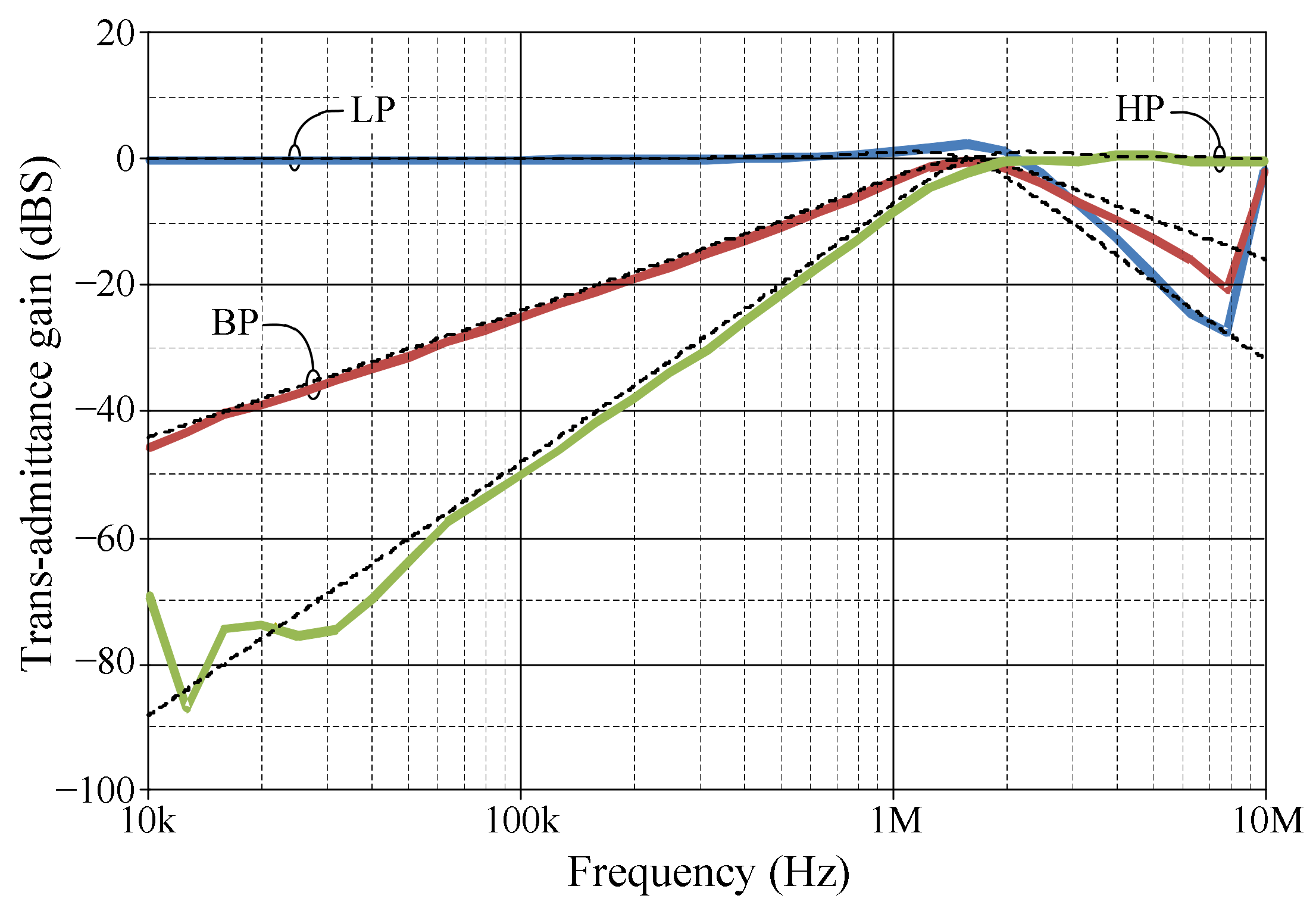
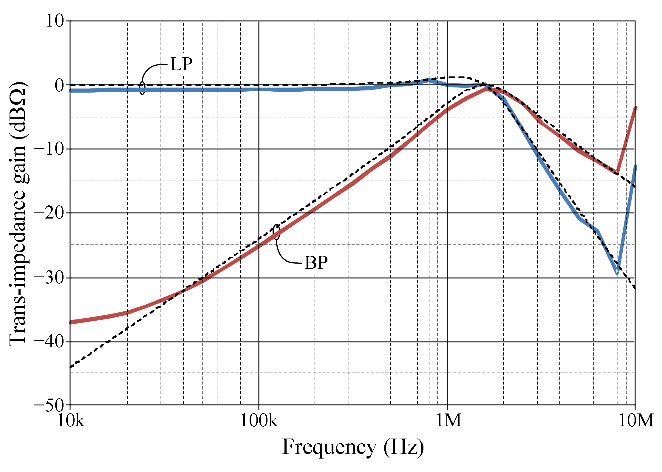
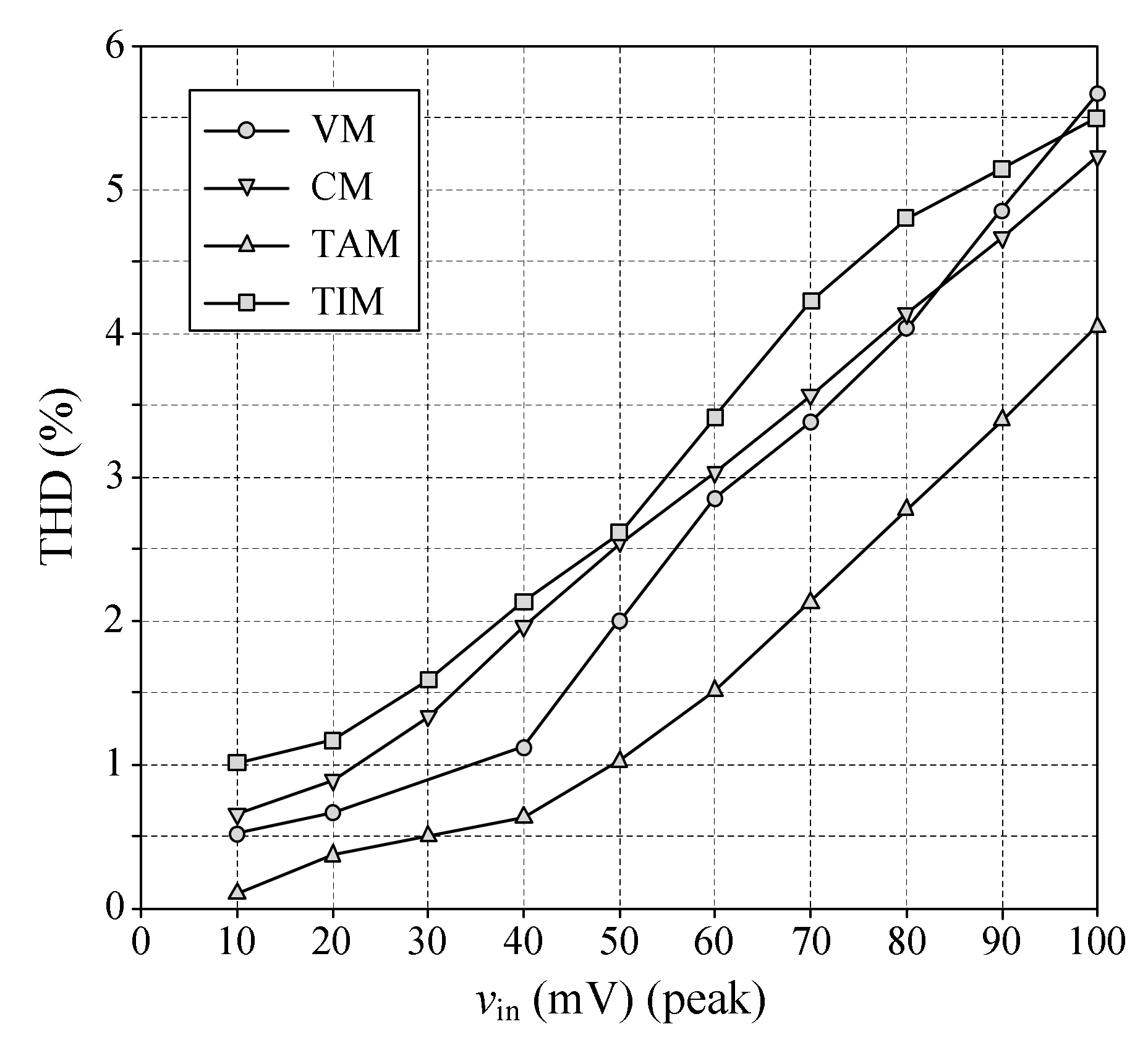
7. Experimental Results
8. Conclusions
Author Contributions
Funding
Institutional Review Board Statement
Informed Consent Statement
Data Availability Statement
Acknowledgments
Conflicts of Interest
Symbols
| α | non-ideal transconductance gain |
| β | non-ideal voltage gain |
| εα | tracking error of transconductance gain |
| εβ | tracking error of voltage gain |
| Kn | transconductance parameter of the transistor |
| µn | mobility of the carriers |
| Cox | gate-oxide capacitance per unit area |
| W | effective channel width |
| L | effective channel length |
| Ω | Ohm |
| dBV | voltage decibel |
| dBA | ampere decibel |
| dBS | siemens decibel |
| dBΩ | Ohm decibel |
| dBc | decibels relative to the carrier |
| V/Hz1/2 | the unit of a noise voltage |
| A/Hz1/2 | the unit of a noise current |
References
- Abuelma’Atti, M.T.; Bentrcia, A. A Novel Mixed-Mode OTA-C Filter. Frequenz 2003, 57, 157–159. [Google Scholar] [CrossRef]
- Abuelma’Atti, M.T. A Novel Mixed-Mode Current-Controlled Current-Conveyor-Based Filter. Act. Passiv. Electron. Components 2003, 26, 185–191. [Google Scholar] [CrossRef]
- Abuelma’atti, M.T.; Bentrcia, A. A novel mixed-mode CCII-based filter. Act. Passiv. Electron. Compon. 2004, 27, 197–205. [Google Scholar] [CrossRef]
- Abuelma’Atti, M.T.; Bentrcia, A.; Al-Shahrani, S.M. A novel mixed-mode current-conveyor-based filter. Int. J. Electron. 2004, 91, 191–197. [Google Scholar] [CrossRef]
- Singh, V.K.; Singh, A.K.; Bhaskar, D.R.; Senani, R. Novel mixed-mode universal biquad configuration. IEICE Electron. Express 2005, 2, 548–553. [Google Scholar] [CrossRef]
- Shah, N.A.; Malik, M.A. Multifunction mixed-mode filter using FTFNs. Analog. Integr. Circuits Signal Process. 2006, 47, 339–343. [Google Scholar] [CrossRef]
- Pandey, N.; Paul, S.K.; Bhattacharyya, A.; Jain, S.B. A new mixed mode biquad using reduced number of active and passive elements. IEICE Electron. Express 2006, 3, 115–121. [Google Scholar] [CrossRef]
- Lee, C.-N.; Chang, C.-M. Single FDCCII-based mixed-mode biquad filter with eight outputs. AEU-Int. J. Electron. Commun. 2009, 63, 736–742. [Google Scholar] [CrossRef]
- Zhijun, L. Mixed-mode universal filter using MCCCII. AEU-Int. J. Electron. Commun. 2009, 63, 1072–1075. [Google Scholar] [CrossRef]
- Minaei, S.; Ibrahim, M.A. A mixed-mode KHN-biquad using DVCC and grounded passive elements suitable for direct cascading. Int. J. Circuit Theory Appl. 2009, 37, 793–810. [Google Scholar] [CrossRef]
- Chen, H.-P.; Liao, Y.-Z.; Lee, W.-T. Tunable mixed-mode OTA-C universal filter. Analog. Integr. Circuits Signal Process. 2008, 58, 135–141. [Google Scholar] [CrossRef]
- Horng, J.W. High-order current-mode and transimpedance-mode universal filters with multiple-inputs and two-outputs us-ing MOCCIIs. Radioengineering 2009, 18, 537–543. [Google Scholar]
- Lee, C.-N. Multiple-Mode OTA-C Universal Biquad Filters. Circuits Syst. Signal Process. 2009, 29, 263–274. [Google Scholar] [CrossRef]
- Pandey, N.; Paul, S.K.; Bhattacharyya, A.; Jain, S.B. Realization of generalized mixed mode universal filter using CCCIIs. J. Act. Passiv. Electron. Devices 2010, 5, 279–293. [Google Scholar]
- Singh, S.V.; Maheshwari, S.; Chauhan, D.S. Electronically tunable current/voltage-mode universal biquad filter using CCCCTA. Int. J. Recent Trends Eng. Technol. 2010, 3, 71–76. [Google Scholar]
- Yuce, E. Fully integrable mixed-mode universal biquad with specific application of the CFOA. AEU-Int. J. Electron. Commun. 2010, 64, 304–309. [Google Scholar] [CrossRef]
- Maheshwari, S.; Singh, S.; Chauhan, D. Electronically tunable low-voltage mixed-mode universal biquad filter. IET Circuits Devices Syst. 2011, 5, 149–158. [Google Scholar] [CrossRef]
- Liao, W.B.; Gu, J.C. SIMO type universal mixed-mode biquadratic filter. Indian J. Eng. Mater. Sci. 2011, 18, 443–448. [Google Scholar]
- Singh, S.V.; Maheshwari, S.; Chauhan, D.S. Single MO-CCCCTA-based electronically tunable cur-rent/trans-impedance-mode biquad universal filter. Circuits Syst. 2011, 2, 1–6. [Google Scholar] [CrossRef]
- Pandey, N.; Paul, S.K. Mixed mode universal filter. J. Circuits Syst. Comput. 2013, 22, 1250064. [Google Scholar] [CrossRef]
- Yeşil, A.; Kaçar, F. Electronically tunable resistorless mixed mode biquad filters. Radioengineering 2013, 22, 1016–1025. [Google Scholar]
- Lee, C.-N. Independently tunable mixed-mode universal biquad filter with versatile input/output functions. AEU-Int. J. Electron. Commun. 2016, 70, 1006–1019. [Google Scholar] [CrossRef]
- Lee, C.-N. Mixed-Mode Universal Biquadratic Filter with No Need of Matching Conditions. J. Circuits Syst. Comput. 2016, 25, 1650106. [Google Scholar] [CrossRef]
- Singh, S.V.; Tomar, R.S.; Chauhan, D.S. A new electronically tunable universal mixed-mode biquad filter. J. Eng. Res. 2016, 4, 44–64. [Google Scholar] [CrossRef]
- Singh, D.; Afzal, N. Fully Digitally Programmable Generalized Mixed Mode Universal Filter Configuration. Circuits, Syst. Signal Process. 2015, 35, 1457–1480. [Google Scholar] [CrossRef]
- Pandey, R.; Pandey, N.; Singhal, N. Single VDTA Based Dual Mode Single Input Multioutput Biquad Filter. J. Eng. 2016, 2016, 1–10. [Google Scholar] [CrossRef]
- Singh, D.; Afzal, N. Digitally programmable mixed mode universal filter using followers-a minimal realization. Analog. Integr. Circuits Signal Process. 2015, 86, 289–298. [Google Scholar] [CrossRef]
- Chen, H.-P.; Yang, W.-S. Electronically Tunable Current Controlled Current Conveyor Transconductance Amplifier-Based Mixed-Mode Biquadratic Filter with Resistorless and Grounded Capacitors. Appl. Sci. 2017, 7, 244. [Google Scholar] [CrossRef]
- Chamnanphai, V.; Sa-Ngiamvibool, W. Electronically tunable SIMO mixed-mode universal filter using VDTAs. Prz. Elektrotech. 2017, 93, 207–211. [Google Scholar] [CrossRef]
- Parvizi, M.; Taghizadeh, A.; Mahmoodian, H.; Kozehkanani, Z.D. A Low-Power Mixed-Mode SIMO Universal Gm–C Filter. J. Circuits Syst. Comput. 2017, 26, 1750164. [Google Scholar] [CrossRef]
- Horng, J.W.; Wu, C.M.; Herencsar, N. Current-mode and transimpedance-mode universal biquadratic filter using two cur-rent conveyors. Indian J. Eng. Mater. Sci. 2017, 24, 461–468. [Google Scholar]
- Cini, U.; Aktan, M. Dual-mode OTA based biquadratic filter suitable for current-mode applications. AEU-Int. J. Electron. Commun. 2017, 80, 43–47. [Google Scholar] [CrossRef]
- Faseehuddin, M.; Sampe, J.; Shireen, S.; Ali, S.H.M. A novel mix-mode universal filter employing a single active element and minimum number of passive components. Inf. MIDEM 2017, 47, 211–221. [Google Scholar]
- Sampe, J.; Faseehuddin, M.; Ali, S.H.M. DOCCCII based minimum component mix mode universal filter. Int. J. Advances Sci. Eng. Tech. 2017, 5, 17–22. [Google Scholar]
- Chaturvedi, B.; Mohan, J.; Kumar, A. A new versatile universal biquad configuration for emerging signal processing applications. J. Circuits Syst. Comput. 2018, 27, 1850196. [Google Scholar] [CrossRef]
- Tsukutani, T.; Yabuki, N. A DVCC-Based Mixed-Mode Biquadratic Circuit. J. Electr. Eng. 2018, 6, 52–56. [Google Scholar] [CrossRef]
- Channumsin, O.; Tangsrirat, W. Dual-mode multifunction filter using VDGAs. In Proceedings of the International Conference on Electrical Engineering/Electronics, Computer, Telecommunications and Information Technology (ECTI-CON), Chiang Rai, Thailand, 18–21 July 2018. [Google Scholar] [CrossRef]
- Safari, L.; Barile, G.; Ferri, G.; Stornelli, V. A New Low-Voltage Low-Power Dual-Mode VCII-Based SIMO Universal Filter. Electronics 2019, 8, 765. [Google Scholar] [CrossRef]
- Albrni, M.A.; Faseehuddin, M.; Sampe, J.; Ali, S.H.M. Novel Dual Mode Multifunction Filter Employing Highly Versatile VD-DXCC. Inf. MIDEM-J. Microelectron. Electron. Components Mater. 2019, 49, 167–176. [Google Scholar] [CrossRef]
- Bhaskar, D.R.; Raj, A.; Kumar, P. Mixed-Mode Universal Biquad Filter Using OTAs. J. Circuits Syst. Comput. 2019, 29, 2050162. [Google Scholar] [CrossRef]
- Lee, C.-N.; Yang, W.-C. General Mixed-Mode Single-Output DDCC-based Universal Biquad Filter. Int. J. Eng. Res. 2020, 9, 744–749. [Google Scholar] [CrossRef]
- Albrni, M.I.A.; Mohammad, F.; Herencsar, N.; Sampe, J.; Ali, S.H.M. Novel electronically tunable biquadratic mixed-mode universal filter capable of operating in MISO and SIMO configurations. Inf. MIDEM 2020, 50, 189–203. [Google Scholar] [CrossRef]
- Tangsrirat, W.; Pukkalanun, T.; Channumsin, O. Single VDGA-based dual-mode multifunction biquadratic filter and quad-rature sinusoidal oscillator. Inf. MIDEM 2020, 50, 125–136. [Google Scholar] [CrossRef]
- Albrni, M.A.; Sampe, J.; Ali, S.H.M.; Zain, A.R.M. Design of VD-DDCC for novel dual mode universal filter with grounded passive components. Int. J. Nanoelectron. Mater. 2020, 13, 259–266. [Google Scholar]
- Faseehuddin, M.; Herencsar, N.; Albrni, M.A.; Sampe, J. Electronically tunable mixed-mode universal filter employing a sin-gle active block and a minimum number of passive components. Appl. Sci. 2021, 11, 55. [Google Scholar] [CrossRef]
- Agrawal, D.; Maheshwari, S. High-Performance Electronically Tunable Analog Filter Using a Single EX-CCCII. Circuits Syst. Signal Process. 2020, 40, 1127–1151. [Google Scholar] [CrossRef]
- Biolek, D.; Senani, R.; Biolkova, V.; Kolka, Z. Active elements for analog signal processing: Classification, review, and new proposals. Radioengineering 2008, 17, 15–32. [Google Scholar]
- Sotner, R.; Jerabek, J.; Herencsar, N. Voltage differencing buffered/inverted amplifiers and their applications for signal gen-eration. Radioengineering 2013, 22, 490–504. [Google Scholar]
- Tangsrirat, W. Actively Floating Lossy Inductance Simulators Using Voltage Differencing Buffered Amplifiers. IETE J. Res. 2018, 65, 446–459. [Google Scholar] [CrossRef]
- Biolkova, V.; Kolka, Z.; Biolek, D. Fully balanced voltage differencing buffered amplifier and its applications. In Proceedings of the IEEE International Midwest Symposium on Circuits and Systems, Cancun, Mexico, 2–5 August 2009. [Google Scholar] [CrossRef]
- Kaçar, F.; Yeşil, A.; Noori, A. New CMOS realization of voltage differencing buffered amplifier and its biquad filter applications. Radioengineering 2012, 21, 333–339. [Google Scholar]
- Ismael, A.R. CMOS implementation of VDBA to design symmetric filters. J. Multidiscip. Eng. Sci. Tech. 2016, 3, 4178–4181. [Google Scholar]
- Ismael, A.R. The applications employed to design a new kind of filter using the active element (VDBA). Kirkuk Univ. J. Scientific Stud. 2016, 11, 287–303. [Google Scholar] [CrossRef]
- Gupta, P.; Pandey, R. Single VDBA based Multifunction Filter. Int. J. Control Theory Appl. 2017, 10, 651–661. [Google Scholar]
- Başak, M.E.; Kaçar, F. Ultra-low voltage VDBA design by using PMOS DTMOS transistors. IU-J. Electr. Electron. Eng. 2017, 17, 3463–3469. [Google Scholar]
- Yadav, C.K.; Prasad, D.; Haseeb, Z.; Laxya; Kumar, M. CM-Biquad Filter Using Single DO-VDBA. Circuits Syst. 2018, 9, 133–139. [Google Scholar] [CrossRef][Green Version]
- Roongmuanpha, N.; Pukkalanun, T.; Tangsrirat, W. Practical realization of electronically adjustable universal filter using commercially available IC-based VDBA. Eng. Rev. 2021, 41, 247933. [Google Scholar] [CrossRef]
- Mamatov, I.; Özçelep, Y.; Kaçar, F. Voltage differencing buffered amplifier based low power, high frequency and universal filters using 32 nm CNTFET technology. Microelectron. J. 2020, 107, 104948. [Google Scholar] [CrossRef]
- Linear Technology, LT1228: 100 MHz Current Feedback Amplifier with DC Gain Control. Available online: https://www.analog.com/media/en/technical-documentation/data-sheets/1228fd.pdf (accessed on 9 September 2021).


| Related Works/ Year | Configuration | Number of Components Used | Filter Functions Realized | Grounded Passive Elements | Inbuilt Tunability | Independent Control of ωo and Q | Need for Inverting or Double Input Signal(s) | ||||
|---|---|---|---|---|---|---|---|---|---|---|---|
| Active | Passive | VM | CM | TAM | TIM | ||||||
| [1]/2003 | MISO | OTA = 6 | C = 2 | all five | all five | -- | -- | yes | yes | no | no |
| [2]/2003 | MIMO | DO-CCCII = 4 | C = 2 | LP, BP, HP | LP, BP, HP | LP, BP, HP, BS | LP, BP, HP | yes | yes | yes | no |
| [3]/2004 | MISO | CCII = 5 | R = 7, C = 2 | all five | all five | all five | all five | no | no | yes | no |
| [4]/2004 | MISO | CCII = 6, DO-CCII = 1 | R = 8, C = 2 | all five | all five | all five | all five | no | no | yes | yes |
| [5]/2005 | SIMO | CFOA = 4 | R = 9, C = 2, switch = 1 | all five | all five | all five | all five | no | no | no | no |
| [6]/2006 | SIMO | FTFN = 3 | R = 3, C = 2 | LP, BP, HP | LP, BP, HP | BP, HP | LP, BP | no | no | no | no |
| [7]/2006 | MISO | CCII = 3 | R = 4, C = 2, switch = 2 | all five | all five | all five | all five | no | no | no | no |
| [8]/2009 | SIMO/MISO | FDCCII = 1 | R = 3, C = 2 | all five | all five | BP, HP | all five | no | no | yes | no |
| [9]/2009 | SIMO | MO-CCCII = 5 | C = 2 | LP, BP, HP | LP, BP, HP | LP, BP, HP | LP, BP, HP | yes | yes | yes | no |
| [10]/2009 | SIMO | DVCC = 3 | R = 3, C = 2, MOS = 6 | LP, BP, BS | all five | all five | LP, BP | yes | no | yes | no |
| [11]/2009 | MISO | OTA = 5 | C = 2 | all five | all five | all five | all five | yes | yes | yes | yes |
| [12]/2009 | MISO | MO-CCII = 3 | R = 3, C = 2 | -- | all five | -- | all five | no | no | no | no |
| [13]/2010 | MISO | OTA = 3, DO-OTA = 1, MO-OTA = 1 | C = 2 | all five | all five | all five | all five | yes | yes | no | yes |
| [14]/2010 | MISO/MIMO | DO-CCCII = 2 | R = 2, C = 2 | all five | all five | all five | all five | no | yes | yes | no |
| [15]/2010 | SIMO | CCCCTA = 2 | C = 2 | LP, BP | all five | all five | LP, BP | no | yes | no | no |
| [16]/2010 | MISO/MIMO | SCFOA = 1 | R = 3, C = 2 | all five | LP, BP, BS | -- | -- | no | no | no | yes |
| [17]/2011 | SIMO | CCCCTA = 3 | C = 2 | LP, BP, HP | all five | all five | LP, BP, HP | yes | yes | no | no |
| [18]/2011 | SIMO | DDCC = 3 | R = 4, C = 2 | all five | all five | all five | all five | no | no | yes | no |
| [19]/2011 | MISO | MO-CCCCTA = 1 | C = 2 | -- | all five | -- | all five | yes | yes | no | no |
| [20]/2013 | MIMO | MO-CCCII = 4 | C = 2 | all five | all five | all five | all five | yes | yes | no | yes |
| [21]/2013 | MISO/MIMO | VDTA = 2 | C = 2 | all five | -- | all five | -- | no | yes | yes | no |
| [22]/2016 | MIMO | FDCCII = 1, DDCC = 1 | R = 6, C = 2 | all five | all five | all five | all five | no | no | yes | yes |
| [23]/2016 | MIMO | FDCCII = 2 | R = 5, C = 2 | all five | all five | all five | all five | no | no | no | no |
| [24]/2016 | MISO/MIMO | MCCTA = 1 | R = 2, C = 2 | all five | all five | all five | all five | no | yes | yes | no |
| [25]/2016 | MISO | DP-CCII = 6, MO-CCII = 2 | R = 4, C = 2 | all five | all five | all five | all five | yes | no | yes | yes |
| [26]/2016 | SIMO | VDTA = 1 | R = 1, C = 3 | LP, BP, HP | LP, BP, HP | -- | -- | no | yes | yes | no |
| [27]/2016 | SISO | DPCF = 5, VF = 2 | R = 4, C = 2, switch = 3 | all five | all five | all five | all five | no | yes | yes | no |
| [28]/2017 | SIMO | CCCCTA = 3 | C = 2 | all five | all five | all five | LP, BP, HP | yes | yes | yes | no |
| [29]/2017 | SIMO | VDTA = 3 | C = 2 | LP, BP, HP | -- | all five | -- | yes | yes | yes | no |
| [30]/2017 | SIMO | OTA = 3, MO-OTA = 3 | C = 2 | all five | all five | all five | all five | yes | yes | no | no |
| [31]/2017 | SIMO | DVCC = 1, MO-CCII = 1 | R = 4, C = 2 | -- | all five | -- | all five | no | no | yes | no |
| [32]/2017 | SIMO | OTA = 1, MO-OTA = 3 | C = 2, switch = 1 | -- | LP, BP, HP | LP, BP, HP | -- | yes | yes | yes | no |
| [33]/2017 | MISO | DXCCDITA = 1 | R = 2, C = 2 | all five | all five | BP, HP | all five | no | yes | no | yes |
| [34]/2017 | MISO | DO-CCCII = 2 | R = 1, C = 2 | all five | all five | BP, HP | all five | no | yes | no | yes |
| [35]/2018 | SIMO | FDCCII = 2 | R = 4, C = 2 | all five | all five | all five | all five | no | no | yes | no |
| [36]/2018 | MISO | DVCC = 5 | R = 5, C = 2 | all five | all five | all five | all five | yes | no | yes | no |
| [37]/2018 | SIMO | VDGA = 2 | C = 3 | LP, BP, HP | LP, BP, HP | -- | -- | no | yes | no | no |
| [38]/2019 | SIMO | VCII = 3, I-CB = 1 | R = 3, C = 3 | LP, BP, HP | HP, BS, AP | LP, BP, HP | LP, BP, HP | no | no | no | no |
| [39]/2019 | MISO | VD-DXCC = 1 | R = 2, C = 2 | all five | all five | -- | -- | no | yes | yes | yes |
| [40]/2020 | MISO | OTA = 5 | C = 2 | all five | all five | all five | all five | yes | yes | yes | no |
| [41]/2020 | MISO/MIMO | DDCC = 3 | R = 4, C = 2 | all five | all five | all five | all five | no | no | no | no |
| [42]/2020 | SIMO/MISO | EXCCTA = 2 | R = 4, C = 2, switch = 1 | all five | all five | all five | all five | no | yes | yes | no |
| [43]/2020 | SIMO | VDGA = 1 | R = 2, C = 2 | LP, BP, HP | LP, BP, HP | -- | -- | no | yes | yes | no |
| [44]/2020 | MISO | VD-DDCC = 2 | R = 3, C = 2 | all five | -- | all five | -- | yes | yes | yes | no |
| [45]/2021 | MISO/MIMO | VD-EXCCII = 1 | R = 3, C = 2 | all five | all five | all five | all five | no | yes | yes | no |
| [46]/2021 | MISO/MIMO | EX-CCCII = 1 | R = 1, C = 2 | all five | all five | all five | BP, HP | no | yes | yes | yes |
| Proposed circuit | MISO/ SIMO | VDBA = 2 | R = 2, C = 2 | all five | all five | all five | LP, BP | yes (except for VM) | yes | yes | no |
| Related Works/ Year | Configuration | Number of Components Used | Filter Functions Realized | Grounded Passive Elements | Inbuilt Tunability | Independent Control of ωo and Q | Need for Inverting or Double Input Signal(s) | ||||
|---|---|---|---|---|---|---|---|---|---|---|---|
| Active | Passive | VM | CM | TAM | TIM | ||||||
| [50]/2009 | SIMO | FB-VDBA = 2 | R = 4, C = 2 | LP, BP, HP | -- | BP, HP | -- | no | yes | no | no |
| [51]/2012 | MISO | VDBA = 2 | Figure 3: C = 2 | all five | -- | -- | -- | no | yes | no | yes |
| Figure 4: R = 1, C = 2 | all five | -- | -- | -- | no | yes | yes | no | |||
| [52]/2016 | MISO | VDBA = 2 | C = 2 | all five | -- | -- | -- | no | yes | no | yes |
| [53]/2016 | MISO | VDBA = 2 | C = 2 | all five | -- | -- | -- | no | yes | no | yes |
| [54]/2017 | SISO | VDBA = 1 | R = 3-4, C = 2 | LP, BP, HP | -- | -- | -- | no | yes | yes | no |
| [55]/2017 | MIMO | VDBA = 2 | C = 2 | LP, BP, HP, BS | -- | -- | -- | no | yes | no | no |
| [56]/2018 | SIMO | DO-VDBA = 1 | R = 2, C = 2 | -- | all five | -- | -- | no | yes | yes | no |
| [57]/2020 | MISO | VDBA = 2 | C = 2 | all five | -- | -- | -- | no | yes | yes | yes |
| [58]/2021 | MISO | VDBA = 2 | C = 2 | LP, BP, HP, BS | -- | -- | -- | no | yes | yes | no |
| Proposed circuit | MISO/ SIMO | VDBA = 2 | R = 2, C = 2 | all five | all five | all five | LP, BP | yes (except for VM) | yes | yes | no |
| Transistors | W(µm)/L(µm) |
|---|---|
| M1-M2, M5, M7-M8, M12-M13 | 2.4/0.18 |
| M3, M9, M14 | 5/0.18 |
| M4, M10 | 5.2/0.18 |
| M6 | 3.25/0.18 |
| M11 | 10/0.18 |
| IB = IB1 = IB2 (µA) | gm = gm1 = gm2 (mA/V) | R2 (kΩ) | fo (MHz) | Deviation in fo (%) | |
|---|---|---|---|---|---|
| Ideal Value | Simulated Value | ||||
| 30 | 0.37 | 25.7 | 1.12 | 1.09 | 2.67 |
| 100 | 0.67 | 14 | 2.15 | 2.24 | 4.18 |
| 300 | 1.17 | 8.12 | 3.72 | 3.52 | 5.38 |
Publisher’s Note: MDPI stays neutral with regard to jurisdictional claims in published maps and institutional affiliations. |
© 2021 by the authors. Licensee MDPI, Basel, Switzerland. This article is an open access article distributed under the terms and conditions of the Creative Commons Attribution (CC BY) license (https://creativecommons.org/licenses/by/4.0/).
Share and Cite
Roongmuanpha, N.; Faseehuddin, M.; Herencsar, N.; Tangsrirat, W. Tunable Mixed-Mode Voltage Differencing Buffered Amplifier-Based Universal Filter with Independently High-Q Factor Controllability. Appl. Sci. 2021, 11, 9606. https://doi.org/10.3390/app11209606
Roongmuanpha N, Faseehuddin M, Herencsar N, Tangsrirat W. Tunable Mixed-Mode Voltage Differencing Buffered Amplifier-Based Universal Filter with Independently High-Q Factor Controllability. Applied Sciences. 2021; 11(20):9606. https://doi.org/10.3390/app11209606
Chicago/Turabian StyleRoongmuanpha, Natchanai, Mohammad Faseehuddin, Norbert Herencsar, and Worapong Tangsrirat. 2021. "Tunable Mixed-Mode Voltage Differencing Buffered Amplifier-Based Universal Filter with Independently High-Q Factor Controllability" Applied Sciences 11, no. 20: 9606. https://doi.org/10.3390/app11209606
APA StyleRoongmuanpha, N., Faseehuddin, M., Herencsar, N., & Tangsrirat, W. (2021). Tunable Mixed-Mode Voltage Differencing Buffered Amplifier-Based Universal Filter with Independently High-Q Factor Controllability. Applied Sciences, 11(20), 9606. https://doi.org/10.3390/app11209606