Article

Role of the Binding Motifs in the Energy Level Alignment and Conductance of Amine-Gold Linked Molecular Junctions within DFT and DFT + Σ

Institute of Physics, Czech Academy of Sciences, Cukrovarnická 10, Prague 16200, Czech Republic
*
Authors to whom correspondence should be addressed.
Appl. Sci. 2021, 11(2), 802; https://doi.org/10.3390/app11020802
Submission received: 24 December 2020 / Revised: 12 January 2021 / Accepted: 13 January 2021 / Published: 15 January 2021
(This article belongs to the Special Issue Molecular Electronics)

Abstract

:
We investigate, using density functional theory (DFT), the electronic and conducting properties of benzenediamine connected to gold electrodes via different tip structures. We examine a series of binding motifs to the electrodes and calculate the junction spectral properties. We consider corrections to the position of molecular resonances at the junction and discuss different approaches to the calculation of these shifts. We relate the magnitude of these corrections to resonance energies to the atomistic structure of the tip. Benzenediamine DFT-based transmission spectra can be well approximated by a Lorentzian model involving only the highest occupied molecular orbital (HOMO). We show how benzenediamine calculated conductance values in quantitative agreement with previous experiments can be achieved from the combination of DFT-based spectra and corrections to the DFT-based HOMO energy and an accessible Lorentzian model.

1. Introduction

Understanding and controlling charge transport in single molecule junctions have been important since it was first suggested that a single molecule might function as an active electronic component [1], and therefore, that metal–organic interfaces are building blocks for the next generation of electronic devices [2,3]. Charge transport properties are mainly measured using scanning-probe methods, in particular, scanning tunneling microscopy break junctions (STM-BJ) [4,5], and mechanically-controlled microscopy break junctions (MC-BJ) [6,7]. Such measurements are typically carried out in solution and at room temperature, and data from thousands of measurements are compiled to generate conductance histograms [8,9,10]. However, in those experiments, the geometry of the interface on the atomic scale is not known, as it cannot be measured in situ, and it is also changing during the experiment, or from sample to sample. Therefore, theoretical methods to understand and guide experiments are extremely valuable [3,11].
Density functional theory (DFT) is the fundamental approach to calculate the electronic properties and optimize the geometry of the junction [12,13]. Similarly, electron transport calculations are normally performed within the non-equilibrium Green’s function (NEGF) formalism. DFT-NEGF, even at zero bias (DFT-Landauer), has been able to correctly reproduce trends in conductance with the correct physical picture [14,15,16,17,18,19,20]. However, despite the significant progress that DFT simulations have offered, their limitations are well known. Among them, perhaps the most relevant for electron transport is the underestimation of the fundamental energy gap at the metal/molecule interface [21,22,23,24]. To go beyond the semi-quantitative picture provided by DFT, it would be desirable to make quantitative comparisons with experimentally measured conductance. For this, corrections to the DFT electronic structure at the interface need to be made. The most widely used approach is the DFT + Σ method [25,26,27,28,29,30,31], where corrections to conducting orbital(s) are calculated externally and added onto the converged system Hamiltonian after the DFT cycle. The correction is a self-energy composed of two terms: one that corrects the molecular gas-phase and one that accounts for the nonlocal polarization due the metal electrodes [25,32,33].
A typical molecular junction is composed of a single molecule bonded to electrodes on either side using chemical linker groups. Electrodes are generally metallic, and Au has been the most commonly used electrode material in scanning-probe studies because of its inertness, which enables consistent and reproducible measurements over a wide range of conditions [5,34]. Linker groups connect the molecule to the electrodes mechanically and electronically [35]. Depending on their chemical nature, linker groups bind to the electrodes either forming donor-acceptor bonds with surface asperities (for example, amine groups -NH2) [25,36], geometry-dependent binding using pyridine groups (−NC5H5) [37,38], covalent bonding (such as thiol groups −SH) [39,40,41] or through carboxylic groups (−COOH) [42,43]. The atomistic details of the metal–molecule interface have been shown to tune the electronic and conducting properties of the junction [44,45,46,47]. Experimentally, variations in conductance strongly depend on the nature of the linker group. While for thiolate–Au linkers, they are very large [9,47,48,49,50], for amine-terminated molecules, these are significantly smaller [25,26,33,51]. The benzenediamine (BDA)–Au interface is a prototypical metal–molecule structure that has been extensively investigated experimentally [25,33,51] and theoretically [26,27,52,53], and is, therefore, an excellent benchmark. STM-BJ studies of BDA between Au electrodes yield a conductance peak at 6.4 × 10⁻³ G0 [25,51,52].
In this work, we focus on the simulation of Au–BDA–Au junctions and investigate how sensitive the electronic and conducting properties are with respect to the atomistic termination of the Au tip structures between molecules and electrodes. We carry out this analysis using both DFT and DFT + Σ formalisms, where, for the latter, we also discuss in detail the magnitude of the necessary corrections to DFT orbital energies at the junction. This study illustrates, for a range of BDA interface geometries, how simple post-processing corrections to DFT-based transmission properties can achieve very good agreement with measured conductance values.

2. Methods

We employed the well-known SIESTA and TranSIESTA codes [13,54,55,56]. We constructed the junction geometries from the knowledge that the amine groups bind selectively to undercoordinated Au sites on the metal (111) surface [5,25]. We modeled the N-Au contact using three possible motifs consisting of one, three or four Au atoms (corresponding to adatom, trimer or pyramidal tips, respectively) and considered all possible combinations of these motifs. The resulting six structures are shown in Figure 1: adatom–adatom, adatom–trimer, trimer–trimer, adatom–pyramid, trimer–pyramid and pyramid–pyramid. We relaxed the positions of the atoms in the molecule and Au tip atoms until the residual Hellman–Feynman forces fell below 0.02 eV/Å. We used an exchange correlation functional which accounts for van der Waals (vdW) interactions [57]. For structure optimization, the real-space grid was defined with an equivalent energy cut-off of 250 Ry, while the reciprocal space was sampled using a 2 × 2 × 1 Monkhorst-pack mesh. For calculations of density of states, we used a 5 × 5 × 1 Monkhorst-pack grid.
Subsequent calculations of charge transport were performed at zero bias for optimized geometries using the Landauer formalism [58] as implemented by TranSIESTA [13,56]. Au atoms were described using a single-ζ polarized basis set, while a double-ζ polarized basis was used for molecular atoms. In these calculations, 5 × 5 × 1 and 15 × 15 × 1 Monkhorst-pack grids were used in reciprocal space for calculating the Green’s function and transmission spectra, respectively.
We also employed the DFT + Σ method [25,26,27,29,30], which we implemented in SIESTA. In this approach, corrections are added explicitly into the system Hamiltonian (H→H + Σ) by an orbital dependent operator of the form,
Σ = Σ n | ψ n mol ψ n mol | ,
where Σn is the self-energy correction for the nth molecular orbital, and | ψ n mol denotes the wavefunction states of the molecule. These states are calculated from the Hamiltonian of the molecular subspace Hmol, contained into the Hamiltonian of the total system (H). The correction operator (Equation (1)) acts only on the molecular subspace Hmol ⊆ H, by construction [26,33,59,60]. The self-energy operator Σ can be constructed from a separate calculation of the relaxed isolated molecule [27,60] or from the Hamiltonian of the molecular subspace Hmol directly cropped from the converged ground-state Hamiltonian of the junction. Either way, the correction operator is introduced into the total Hamiltonian, which is diagonalized again in order to obtain the corrected electronic properties of the system.
The self-energy correction term consists of two parts that address: (1) the underestimated gap of the isolated molecule in conventional DFT ( Σ n 1 , gas phase correction) and (2) the lack of renormalization due to the metallic electrodes ( Σ n 2 , polarization due to metallic surface). The total correction is the sum of these two contributions which, as discussed below, have opposite signs, i.e., Σn = Σ n 1 + Σ n 2 . In principle, this correction could be calculated for every molecular orbital n. However, since we are interested in conductance, we focused on the region around the Fermi level, and calculated it only for the highest occupied molecular orbital (HOMO) and the lowest unoccupied molecular orbital (LUMO). We applied ΣHOMO to all occupied states and ΣLUMO to all unoccupied states [26,53].
The first contribution to the self-energy, the gas phase correction Σ n 1 , is defined as the difference between the DFT energy level and the quasiparticle energy level. We calculated the ionization potential (IP), i.e., the energy required to remove an electron from the ground state, and the electron affinity (EA), i.e., the energy required to add an electron to the ground state. These quantities are defined in terms of (DFT) total energies as IP = E(N) − E(N − 1), and EA = E(N + 1) − E(N), where E(Ni) is the total energy of the system with Ni electrons [28,29,61]. Furthermore, the gas-phase correction to the HOMO (LUMO) is calculated as a difference between the DFT energy position of the isolated molecule E HOMO DFT ( E LUMO DFT ) and IP (EA),
Σ HOMO 1 = E HOMO DFT - IP ,
Σ LUMO 1 = ( E LUMO DFT EA )
The second term, accounting for the polarization due to the metallic surface Σ n 2 , is approximated by a classical image charge model [32,61]. It is modeled as the potential energy of a point charge distribution between two image planes. We used a point charge qn = 1 for the n = HOMO or LUMO, corresponding to each atom in the molecule. Each point charge qn,i is located at a vertical distance zi from the image plane ztop (zbottom), corresponding to the top (bottom) electrode. Therefore, the self-energy term is calculated as
Σ n 2 = i | q n , i | 2 4 ( z i     z t o p ) + i | q n , i | 2 4 ( z i     z b o t t o m )

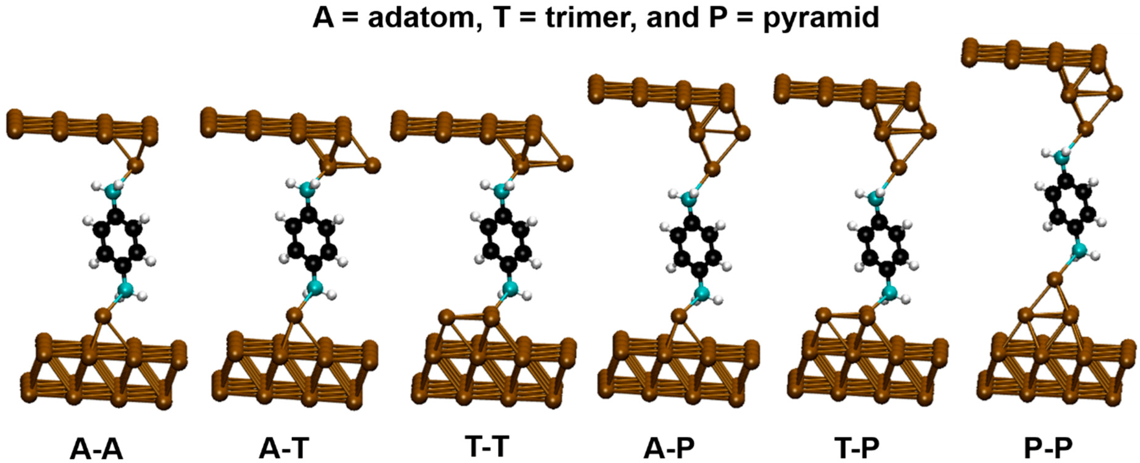
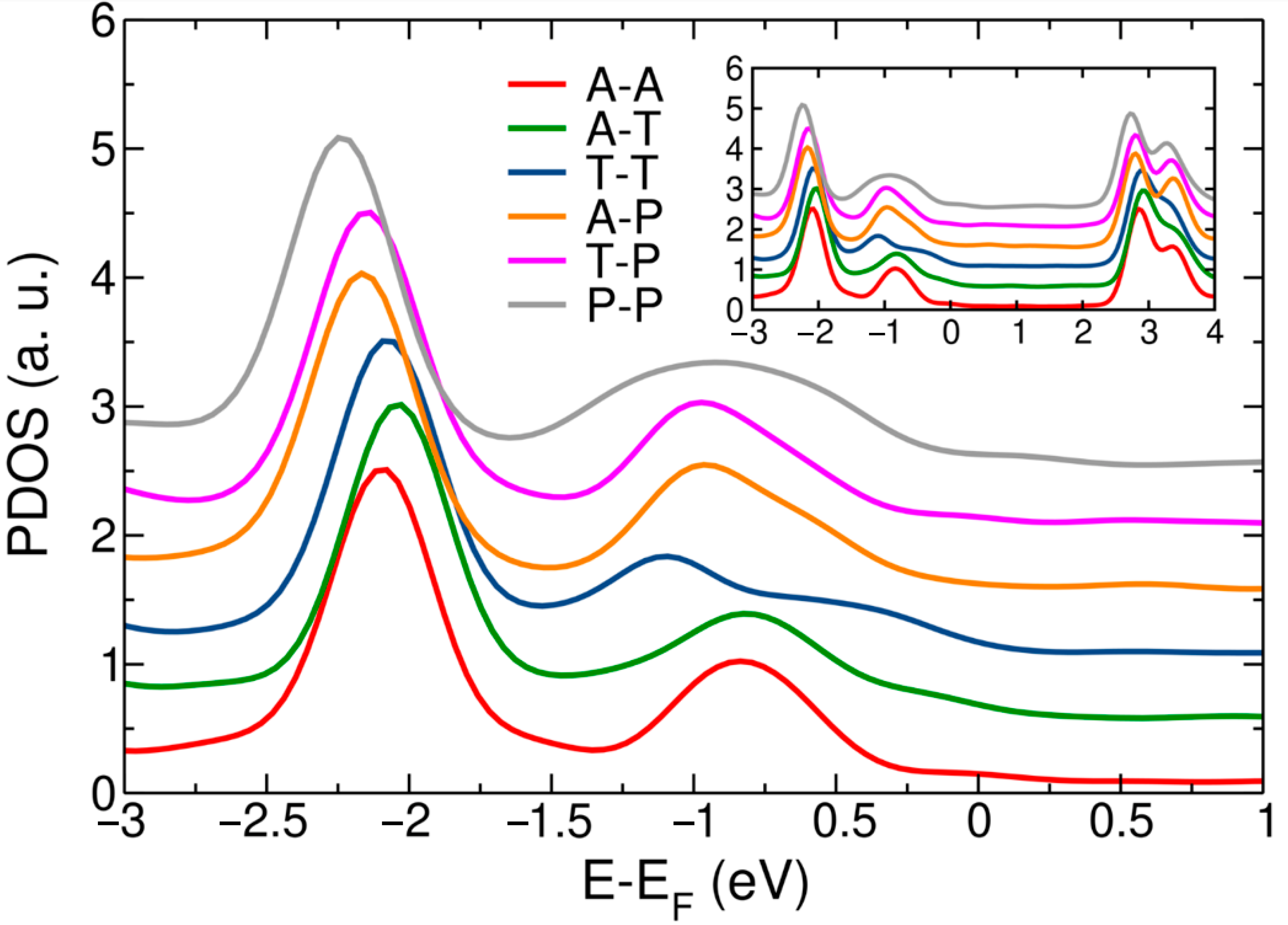
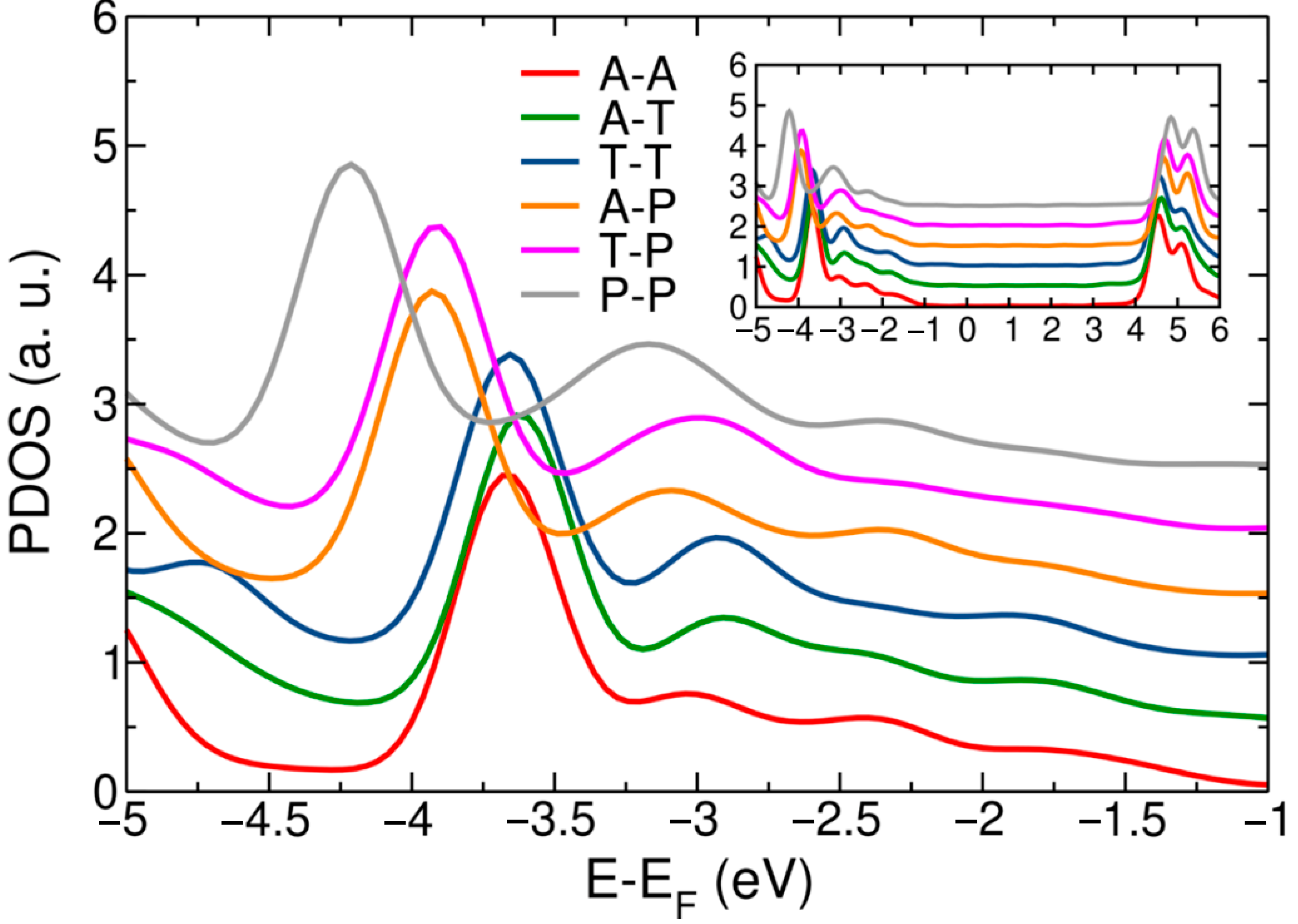
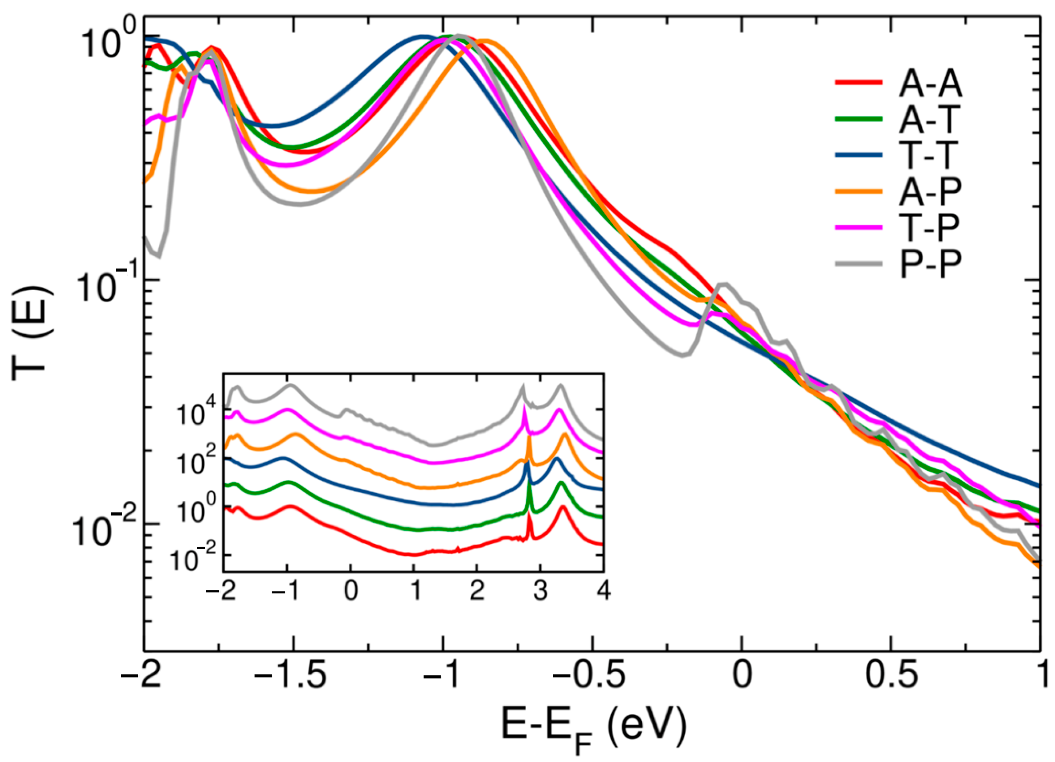
3. Results and Discussion

We began our analysis by studying the electronic properties of the junctions within DFT, as well as their variation with respect to the binding motifs (Figure 1). We focused only on the position of the HOMO peak, as it has been shown in the literature that HOMO dominates the zero-bias conductance for BDA [25,26,51,52]. Figure 2 shows the density of states projected over the atoms of the molecule for all the binding motifs considered: adatom–adatom, adatom–trimer, trimer–trimer, adatom–pyramid, trimer–pyramid and pyramid–pyramid. The figure is centered around the energy of the DFT HOMO peak (−1.0 eV). The inset shows the same data on an extended energy range. The data are offset vertically for clarity. From the figure, the position of the HOMO peak at the DFT level had a small variation across all different structures, ranging from −0.83 to −1.09 eV. The LUMO peak was found between 2.74 and 2.92 eV. From Figure 2, tip structures involving adatoms broadly resulted in sharper PDOS peaks and resonances closer to the Fermi level. In order to implement the DFT + Σ method, it is necessary to calculate the magnitude of the self-energy correction of the appropriate resonance (Equations (2) and (3)). We first address the calculation of the gas-phase self-energy correction of the HOMO peak, Σ HOMO 1 , which involves the calculation of the isolated molecule. Several ways of computing this correction are possible. One option is to optimize the geometry of the molecule. Another possibility is to compute the molecule in the geometry it adopts at the junction. In the case of BDA, the magnitude of both corrections was the same in all cases regardless of which approach was used, −2.99 eV, although we believe that this is due to the reduced conformational flexibility of the amine linker. We anticipated a spread of values for other linkers, such as methyl-sulfide groups, which rotate when adsorbed with respect to their gas-phase geometry. In this case, it would be more consistent to use the geometry the molecule adopts at the junction [20,35].
The second term in the self-energy correction, accounting for the polarization due to the metallic surface, Σ HOMO 2 , was approximated using a classical image charge model, as described in Equation (4). A single point charge was positioned at the geometrical center of the molecule [28,29,53]. The image plane position was taken to be 1.0 Å above the outer atomic plane of each Au [62]. Results for all tip structures are presented in Table 1. The calculated shift of the HOMO resonance due to screening is, for both approaches, given in Table 1. We see that the largest values were obtained for “short” tips that protrude the least from the surface, such as adatoms or trimers. When pyramidal tips were considered, image charge screening was reduced due to the larger vertical distance spanned by these tips.
The total self-energy correction for the HOMO peak is the sum of both (opposing) contributions. Results for all tip structures are presented in Table 2. As expected, the dependence with tip structure is opposite that of Table 1: the largest shift was found for the pyramid–pyramid combination, where the polarization self-energy was lowest, and structures with one pyramid followed. These differences are relevant for the calculation of conductance in subsequent sections. Furthermore, the total self-energy correction for the LUMO peak was 1.90 eV for the adatom–adatom, adatom–trimer and trimer–trimer tip structures, 2.09 eV for the adatom–pyramid and trimer–pyramid tip structures and 2.31 eV for the pyramid–pyramid tip structure.
Having described the spread of the self-energy values with respect to tip structure, we applied the correction to the Hamiltonian (H→H + Σ) as described in Equation (1). The shift was applied to the molecular Hamiltonian. DFT values are given by the eigenstates of the molecular box of the junction Hamiltonian, as described previously. The initial and final (corrected) energies of the HOMO resonance are given in Table 3. Figure 3 shows the corrected density of states projected onto the atoms of the molecule for tip structure combinations. The figure is centered on the range around −3.0 eV, near the position of the corrected HOMO peak. The inset reproduces the same data on a linear scale and over an extended energy range with the curves offset for clarity. The LUMO peak was shifted following the same procedure described here. The position of the corrected HOMO peak ranged between −2.9 and −3.2 eV. Additionally, the position of the corrected LUMO peak ranged between 4.5 and 4.8 eV.
So far, we have focused on the DFT and corrected electronic properties, discussing how to calculate the magnitude of these corrections. In the final section of the paper, we turn to the electron transport properties and how to apply these corrections to DFT-based conductance calculations. Figure 4 shows the transmission spectra of the different BDA junctions calculated using the DFT-Landauer formalism. These calculations take the DFT-based electronic structure as input, with its well-known errors in resonance position. Figure 4 highlights the energy range below the Fermi level where the HOMO resonance, which defines zero-bias conductance, appears at the DFT level. As before, the inset plots the same data on a linear scale over an extended energy range. Figure 4 shows that low-bias conductance is determined by the tailing of the HOMO resonance into the Fermi level [25,26,51,52]. In Figure 4, the HOMO peak position is found between −0.85 and −1.00 eV over the tip structures considered, obviously following the DFT-based density of states (see Figure 2 and Table 3). This is to be compared to the HOMO transmission peak between −0.94 and −1.27 eV reported in the literature [25,26]. Calculated conductance values, given by the transmission at the Fermi level, are given in Table 4. Furthermore, as is common for DFT-based approaches, calculated conductance significantly exceeds the experimental value (6.4 × 10⁻³ G0) [25,51,52], in this case, by about a factor 10.
To improve the agreement between calculated and measured conductance, it is necessary to correct the position of the conducting orbital. The implementation of DFT + Σ in a fully self-consistent DFT-NEGF cycle, out of equilibrium, is far from simple. However, trends can often be drawn from studies in equilibrium. Since in many molecular junctions, conductance takes place due to non-resonant tunneling [3,11,34], it is illustrative to consider simple models involving only one molecular resonance. Although single level models fail when transport involves several molecular orbitals [63] or in cases of quantum interference [64], they nevertheless provide a good starting point for many representative molecular junctions. Different ways of fitting the relevant parameters and their accuracy have been discussed [9,35,44,59,63,64,65,66,67]. Here, we consider a single level (HOMO) at zero bias.
First, the DFT-based conducting peak (in this case HOMO) is fitted using a Lorentzian model of the form,
T ( E ) = A ( ( E     E HOMO ) 2   +   ( Γ / 2 ) 2 ) ,
where EHOMO and A are the HOMO peak position and amplitude, respectively, and Γ is the full width at half maximum. The position of the resonance is then corrected using the self-energy previously addressed (ΣHOMO). This model assumes that width of the Lorentzian (Γ) is unchanged, which is reasonable since DFT captures the electronic coupling well. For the BDA junctions considered, Γ takes three range of values. For adatom–adatom, adatom–trimer and trimer–trimer structures, the widths were 0.51, 0.52, and 0.55 eV, respectively. For adatom–pyramid and trimer–pyramid structures, the widths were 0.43 and 0.45 eV. Finally, for the pyramid–pyramid structure, the width was the lowest, 0.35 eV. This agrees well with previous calculations, where the conductance peak width showed a modest variation between 0.34 to 0.56 eV [25]. The conductance from the Lorentzian fitted curve is presented in Table 4. The agreement with DFT-Landauer values was very good, where the structures with the widest peaks showed a conductance closest to DFT-Landauer.
Table 4 also reports the conductance values calculated from the Lorentzian fit using the DFT + Σ resonance positions. Agreement with experiment was significantly improved. For the adatom–pyramid and trimer–pyramid structures, the corrected conductance was 1.0 × 10⁻² G0. This value still exceeded the experimental conductance, but only for a factor of about 1.6, a substantial improvement as compared to the previous factor of 10. For the adatom–pyramid and trimer–pyramid structures, the corrected conductance was about 6.3 × 10⁻³ G0, which perfectly matches with the experimental value [25,51,52]. Furthermore, for the pyramid–pyramid structure, the corrected conductance was 3.5 × 10⁻³ G0, even falling below the experimental conductance value by a factor of about 1.8. Additionally, the variation between the calculated conductance values among all tip structures was modest, about 18%. This is comparable to the experimental variation of conductance, about 8% [25]. Therefore, the combination of corrections to resonance positions within the DFT + Σ methodology, and a Lorentzian model of conductance, leads to a very good quantitative agreement with measured conductance values of BDA. The approach that we have described here would be of use to calculate the level-corrected conductance for broad classes of molecular junctions from standard DFT-Landauer calculations and rather straightforward corrections to resonance positions, combined with a Lorentzian transport model.

4. Conclusions

We studied the simulation of electronic and charge transport properties of BDA junctions with different tip structures. As is well known, at the DFT level, the HOMO position is too close to the Fermi level, and we discussed corrections to the DFT-based HOMO energy within the DFT + Σ formalism. We discussed the two contributions to the resonance energy correction, arising from the self-energy of the isolated molecule and from the screening at the metallic interface. This correction shifts the HOMO resonance further form the Fermi energy. We found that, for BDA junctions, the first term was not sensitive to the details of its calculations. However, the contribution due to interface screening, which was approximated here by a classical image charge model, did show a substantial variation of several tenths of an eV with tip structure. The total correction to the HOMO resonance at the interface was close to 2 eV towards more negative values. For the interfaces considered, DFT-based transmission spectra of BDA yielded conductance values that significantly overestimate the measured conductance by as much as an order of magnitude. We found that a Lorentzian model considering the HOMO resonance matched the DFT transmission spectra well. We showed that a DFT + Σ approach where this Lorentzian model was combined with the corrected HOMO energy produced a significant improvement in the calculated conductance values. For the different interface structures considered, this approach resulted in values in quantitative agreement with experiments.

Author Contributions

Conceptualization, H.V.; Investigation, E.M.; Methodology, E.M.; Supervision. H.V.; Writing—original draft, E.M.; Writing—review & editing, H.V. All authors have read and agreed to the published version of the manuscript.

Funding

This research was funded by the international mobility MSCA-IF II FZU grant (CZ.02.2.69/0.0/0.0/18_070/0010126) and the Czech Science Foundation GAČR (19-23702S). Computational resources were supplied by the project “e-Infrastruktura CZ” (e-INFRA LM2018140) provided within the program Projects of Large Research, Development and Innovations Infrastructures.

Institutional Review Board Statement

Not applicable.

Informed Consent Statement

Not applicable.

Data Availability Statement

The data presented in this study are available on reasonable request from the corresponding authors.

Conflicts of Interest

The authors declare no conflict of interest.

References

  1. Aviram, A.; Ratner, M.A. Molecular rectifiers. Chem. Phys. Lett. 1974, 29, 277–283. [Google Scholar] [CrossRef]
  2. Nitzan, A.; Ratner, M.A. Electron transport in molecular wire junctions. Science 2003, 300, 1384–1389. [Google Scholar] [CrossRef] [PubMed]
  3. Cuevas, J.C.; Scheer, E. Molecular Electronics: An Introduction to Theory and Experimen; World Scientific: Singapore, 2010; Volume 1, ISBN 978-981-4282-58-1. [Google Scholar]
  4. Xu, B.; Tao, N.J. Measurement of Single-Molecule Resistance by Repeated Formation of Molecular Junctions. Science 2003, 301, 1221–1223. [Google Scholar] [CrossRef] [PubMed] [Green Version]
  5. Venkataraman, L.; Klare, J.E.; Tam, I.W.; Nuckolls, C.; Hybertsen, M.S.; Steigerwald, M.L. Single-molecule circuits with well-defined molecular conductance. Nano Lett. 2006, 6, 458–462. [Google Scholar] [CrossRef] [PubMed] [Green Version]
  6. Tsutsui, M.; Teramae, Y.; Kurokawa, S.; Sakai, A. High-conductance states of single benzenedithiol molecules. Appl. Phys. Lett. 2006, 89, 163111. [Google Scholar] [CrossRef] [Green Version]
  7. Martin, C.A.; Ding, D.; Van Der Zant, H.S.J.; Van Ruitenbeek, J.M. Lithographic mechanical break junctions for single-molecule measurements in vacuum: Possibilities and limitations. New J. Phys. 2008, 10, 65008. [Google Scholar] [CrossRef]
  8. Haiss, W.; Wang, C.; Grace, I.; Batsanov, A.S.; Schiffrin, D.J.; Higgins, S.J.; Bryce, M.R.; Lambert, C.J.; Nichols, R.J. Precision control of single-molecule electrical junctions. Nat. Mater. 2006, 5, 995. [Google Scholar] [CrossRef]
  9. Kim, Y.; Pietsch, T.; Erbe, A.; Belzig, W.; Scheer, E. Benzenedithiol: A Broad-Range Single-Channel Molecular Conductor. Nano Lett. 2011, 11, 3734–3738. [Google Scholar] [CrossRef] [Green Version]
  10. González, M.T.; Wu, S.; Huber, R.; van der Molen, S.J.; Schönenberger, C.; Calame, M. Electrical Conductance of Molecular Junctions by a Robust Statistical Analysis. Nano Lett. 2006, 6, 2238–2242. [Google Scholar] [CrossRef] [Green Version]
  11. Kiguchi, M. Single-Molecule Electronics: An Introduction to Synthesis, Measurement and Theory; Kiguchi, M., Ed.; Springer: Singapore, 2016; ISBN 9789811007248. [Google Scholar]
  12. Kohn, W.; Sham, L.J. Self-Consistent Equations Including Exchange and Correlation Effects. Phys. Rev. 1965, 140, A1133–A1138. [Google Scholar] [CrossRef] [Green Version]
  13. Brandbyge, M.; Mozos, J.L.; Ordejón, P.; Taylor, J.; Stokbro, K. Density-functional method for nonequilibrium electron transport. Phys. Rev. B Condens. Matter Mater. Phys. 2002, 65, 1654011–16540117. [Google Scholar] [CrossRef] [Green Version]
  14. Zang, Y.; Pinkard, A.; Liu, Z.-F.; Neaton, J.B.; Steigerwald, M.L.; Roy, X.; Venkataraman, L. Electronically Transparent Au–N Bonds for Molecular Junctions. J. Am. Chem. Soc. 2017, 139, 14845–14848. [Google Scholar] [CrossRef] [PubMed]
  15. Leary, E.; Zotti, L.A.; Miguel, D.; Márquez, I.R.; Palomino-Ruiz, L.; Cuerva, J.M.; Rubio-Bollinger, G.; González, M.T.; Agrait, N. The Role of Oligomeric Gold–Thiolate Units in Single-Molecule Junctions of Thiol-Anchored Molecules. J. Phys. Chem. C 2018, 122, 3211–3218. [Google Scholar] [CrossRef] [Green Version]
  16. Li, H.; Su, T.A.; Camarasa-Gómez, M.; Hernangómez-Pérez, D.; Henn, S.E.; Pokorný, V.; Caniglia, C.D.; Inkpen, M.S.; Korytár, R.; Steigerwald, M.L.; et al. Silver Makes Better Electrical Contacts to Thiol-Terminated Silanes than Gold. Angew. Chem. Int. Ed. 2017, 56, 14145–14148. [Google Scholar] [CrossRef] [PubMed] [Green Version]
  17. Kuang, G.; Chen, S.Z.; Yan, L.; Chen, K.Q.; Shang, X.; Liu, P.N.; Lin, N. Negative Differential Conductance in Polyporphyrin Oligomers with Nonlinear Backbones. J. Am. Chem. Soc. 2018, 140, 570–573. [Google Scholar] [CrossRef]
  18. Zang, Y.; Ray, S.; Fung, E.-D.; Borges, A.; Garner, M.H.; Steigerwald, M.L.; Solomon, G.C.; Patil, S.; Venkataraman, L. Resonant Transport in Single Diketopyrrolopyrrole Junctions. J. Am. Chem. Soc. 2018, 140, 13167–13170. [Google Scholar] [CrossRef]
  19. Stefani, D.; Weiland, K.J.; Skripnik, M.; Hsu, C.; Perrin, M.L.; Mayor, M.; Pauly, F.; van der Zant, H.S.J. Large Conductance Variations in a Mechanosensitive Single-Molecule Junction. Nano Lett. 2018, 18, 5981–5988. [Google Scholar] [CrossRef]
  20. Schneebeli, S.; Kamenetska, M.; Foss, F.; Vazquez, H.; Skouta, R.; Hybertsen, M.; Venkataraman, L.; Breslow, R. The electrical properties of biphenylenes. Org. Lett. 2010, 12, 4114–4117. [Google Scholar] [CrossRef]
  21. Perdew, J.P.; Levy, M. Physical Content of the Exact Kohn-Sham Orbital Energies: Band Gaps and Derivative Discontinuities. Phys. Rev. Lett. 1983, 51, 1884–1887. [Google Scholar] [CrossRef]
  22. Kümmel, S.; Kronik, L. Orbital-dependent density functionals: Theory and applications. Rev. Mod. Phys. 2008, 80, 3–60. [Google Scholar] [CrossRef] [Green Version]
  23. Kronik, L.; Stein, T.; Refaely-Abramson, S.; Baer, R. Excitation gaps of finite-sized systems from optimally tuned range-separated hybrid functionals. J. Chem. Theory Comput. 2012, 8, 1515–1531. [Google Scholar] [CrossRef] [PubMed]
  24. Sham, L.J.; Schllter, M. Density-functional theory of the energy gap. Phys. Rev. Lett. 1983, 51, 1888–1891. [Google Scholar] [CrossRef]
  25. Quek, S.Y.; Venkataraman, L.; Choi, H.J.; Louie, S.G.; Hybertsen, M.S.; Neaton, J.B. Amine—Gold linked single-molecule circuits: Experiment and theory. Nano Lett. 2007, 7, 3477–3482. [Google Scholar] [CrossRef] [PubMed] [Green Version]
  26. Quek, S.Y.; Choi, H.J.; Louie, S.G.; Neaton, J.B. Length dependence of conductance in aromatic single-molecule junctions. Nano Lett. 2009, 9, 3949–3953. [Google Scholar] [CrossRef]
  27. Li, G.; Rangel, T.; Liu, Z.F.; Cooper, V.R.; Neaton, J.B. Energy level alignment of self-assembled linear chains of benzenediamine on Au(111) from first principles. Phys. Rev. B 2016, 93, 125429. [Google Scholar] [CrossRef] [Green Version]
  28. Markussen, T.; Jin, C.; Thygesen, K.S. Quantitatively accurate calculations of conductance and thermopower of molecular junctions. Phys. Status Solidi Basic Res. 2013, 250, 2394–2402. [Google Scholar] [CrossRef] [Green Version]
  29. Zotti, L.A.; Bürkle, M.; Pauly, F.; Lee, W.; Kim, K.; Jeong, W.; Asai, Y.; Reddy, P.; Cuevas, J.C. Heat dissipation and its relation to thermopower in single-molecule junctions. New J. Phys. 2014, 16, 15004. [Google Scholar] [CrossRef]
  30. Jin, C.; Strange, M.; Markussen, T.; Solomon, G.C.; Thygesen, K.S. Energy level alignment and quantum conductance of functionalized metal-molecule junctions: Density functional theory versus GW calculations. J. Chem. Phys. 2013, 139, 184307. [Google Scholar] [CrossRef] [Green Version]
  31. Jin, C.; Thygesen, K.S. Dynamical image-charge effect in molecular tunnel junctions: Beyond energy level alignment. Phys. Rev. B Condens. Matter Mater. Phys. 2014, 89, 41102. [Google Scholar] [CrossRef] [Green Version]
  32. Neaton, J.B.; Hybertsen, M.S.; Louie, S.G. Renormalization of molecular electronic levels at metal-molecule interfaces. Phys. Rev. Lett. 2006, 97, 216405. [Google Scholar] [CrossRef] [Green Version]
  33. Dell’Angela, M.; Kladnik, G.; Cossaro, A.; Verdini, A.; Kamenetska, M.; Tamblyn, I.; Quek, S.Y.; Neaton, J.B.; Cvetko, D.; Morgante, A.; et al. Relating energy level alignment and amine-linked single molecule junction conductance. Nano Lett. 2010, 10, 2470–2474. [Google Scholar] [CrossRef] [PubMed] [Green Version]
  34. Su, T.A.; Neupane, M.; Steigerwald, M.L.; Venkataraman, L.; Nuckolls, C. Chemical principles of single-molecule electronics. Nat. Rev. Mater. 2016, 1, 16002. [Google Scholar] [CrossRef]
  35. Arasu, N.P.; Vázquez, H. Direct Au-C contacts based on biphenylene for single molecule circuits. Phys. Chem. Chem. Phys. 2018, 20, 10378–10383. [Google Scholar] [CrossRef] [PubMed]
  36. Park, Y.S.; Whalley, A.C.; Kamenetska, M.; Steigerwald, M.L.; Hybertsen, M.S.; Nuckolls, C.; Venkataraman, L. Contact chemistry and single-molecule conductance: A comparison of phosphines, methyl sulfides, and amines. J. Am. Chem. Soc. 2007, 129, 15768–15769. [Google Scholar] [CrossRef]
  37. Kamenetska, M.; Quek, S.Y.; Whalley, A.C.; Steigerwald, M.L.; Choi, H.J.; Louie, S.G.; Nuckolls, C.; Hybertsen, M.S.; Neaton, J.B.; Venkataraman, L. Conductance and Geometry of Pyridine-Linked Single-Molecule Junctions. J. Am. Chem. Soc. 2010, 132, 6817–6821. [Google Scholar] [CrossRef]
  38. Mishchenko, A.; Zotti, L.A.; Vonlanthen, D.; Bürkle, M.; Pauly, F.; Cuevas, J.C.; Mayor, M.; Wandlowski, T. Single-Molecule Junctions Based on Nitrile-Terminated Biphenyls: A Promising New Anchoring Group. J. Am. Chem. Soc. 2011, 133, 184–187. [Google Scholar] [CrossRef]
  39. Tour, J.M.; Jones, L.; Pearson, D.L.; Lamba, J.J.S.; Burgin, T.P.; Whitesides, G.M.; Allara, D.L.; Parikh, A.N.; Atre, S. Self-Assembled Monolayers and Multilayers of Conjugated Thiols, alpha, omega.-Dithiols, and Thioacetyl-Containing Adsorbates. Understanding Attachments between Potential Molecular Wires and Gold Surfaces. J. Am. Chem. Soc. 1995, 117, 9529–9534. [Google Scholar] [CrossRef]
  40. González, M.T.; Leary, E.; García, R.; Verma, P.; Herranz, M.Á.; Rubio-Bollinger, G.; Martín, N.; Agraït, N. Break-Junction Experiments on Acetyl-Protected Conjugated Dithiols under Different Environmental Conditions. J. Phys. Chem. C 2011, 115, 17973–17978. [Google Scholar] [CrossRef]
  41. Inkpen, M.S.; Liu, Z.-F.; Li, H.; Campos, L.M.; Neaton, J.B.; Venkataraman, L. Non-chemisorbed gold–sulfur binding prevails in self-assembled monolayers. Nat. Chem. 2019, 11, 351–358. [Google Scholar] [CrossRef]
  42. Paik, W.; Han, S.; Shin, W.; Kim, Y. Adsorption of Carboxylic Acids on Gold by Anodic Reaction. Langmuir 2003, 19, 4211–4216. [Google Scholar] [CrossRef]
  43. Chen, F.; Li, X.; Hihath, J.; Huang, Z.; Tao, N. Effect of Anchoring Groups on Single-Molecule Conductance:  Comparative Study of Thiol-, Amine-, and Carboxylic-Acid-Terminated Molecules. J. Am. Chem. Soc. 2006, 128, 15874–15881. [Google Scholar] [CrossRef] [PubMed]
  44. Quek, S.Y.; Kamenetska, M.; Steigerwald, M.L.; Choi, H.J.; Louie, S.G.; Hybertsen, M.S.; Neaton, J.B.; Venkataraman, L. Mechanically controlled binary conductance switching of a single-molecule junction. Nat. Nanotechnol. 2009, 4, 230–234. [Google Scholar] [CrossRef] [PubMed] [Green Version]
  45. Su, T.A.; Widawsky, J.R.; Li, H.; Klausen, R.S.; Leighton, J.L.; Steigerwald, M.L.; Venkataraman, L.; Nuckolls, C. Silicon ring strain creates high-conductance pathways in single-molecule circuits. J. Am. Chem. Soc. 2013, 135, 18331–18334. [Google Scholar] [CrossRef] [PubMed]
  46. Kiguchi, M.; Ohto, T.; Fujii, S.; Sugiyasu, K.; Nakajima, S.; Takeuchi, M.; Nakamura, H. Single molecular resistive switch obtained via sliding multiple anchoring points and varying effective wire length. J. Am. Chem. Soc. 2014, 136, 7327–7332. [Google Scholar] [CrossRef] [PubMed]
  47. Kaneko, S.; Montes, E.; Suzuki, S.; Fujii, S.; Nishino, T.; Tsukagoshi, K.; Ikeda, K.; Kano, H.; Nakamura, H.; Vázquez, H.; et al. Identifying the molecular adsorption site of a single molecule junction through combined Raman and conductance studies. Chem. Sci. 2019, 10, 6261–6269. [Google Scholar] [CrossRef] [PubMed] [Green Version]
  48. Paulsson, M.; Krag, C.; Frederiksen, T.; Brandbyge, M. Conductance of Alkanedithiol Single-Molecule Junctions: A Molecular Dynamics Study. Nano Lett. 2009, 9, 117–121. [Google Scholar] [CrossRef]
  49. Isshiki, Y.; Fujii, S.; Nishino, T.; Kiguchi, M. Fluctuation in Interface and Electronic Structure of Single-Molecule Junctions Investigated by Current versus Bias Voltage Characteristics. J. Am. Chem. Soc. 2018, 140, 3760–3767. [Google Scholar] [CrossRef]
  50. Zotti, L.A.; Kirchner, T.; Cuevas, J.-C.; Pauly, F.; Huhn, T.; Scheer, E.; Erbe, A. Revealing the Role of Anchoring Groups in the Electrical Conduction Through Single-Molecule Junctions. Small 2010, 6, 1529–1535. [Google Scholar] [CrossRef] [Green Version]
  51. Venkataraman, L.; Klare, J.E.; Nuckolls, C.; Hybertsen, M.S.; Steigerwald, M.L. Dependence of single-molecule junction conductance on molecular conformation. Nature 2006, 442, 904–907. [Google Scholar] [CrossRef] [Green Version]
  52. Kim, T.; Vázquez, H.; Hybertsen, M.S.; Venkataraman, L. Conductance of molecular junctions formed with silver electrodes. Nano Lett. 2013, 13, 3358–3364. [Google Scholar] [CrossRef]
  53. Chen, Y.; Tamblyn, I.; Quek, S.Y. Energy Level Alignment at Hybridized Organic-Metal Interfaces: The Role of Many-Electron Effects. J. Phys. Chem. C 2017, 121, 13125–13134. [Google Scholar] [CrossRef] [Green Version]
  54. Soler, J.M.; Artacho, E.; Gale, J.D.; García, A.; Junquera, J.; Ordejón, P.; Sánchez-Portal, D. The SIESTA method for ab initio order- N materials simulation. J. Phys. Condens. Matter 2002, 14, 2745. [Google Scholar] [CrossRef] [Green Version]
  55. García, A.; Papior, N.; Akhtar, A.; Artacho, E.; Blum, V.; Bosoni, E.; Brandimarte, P.; Brandbyge, M.; Cerdá, J.I.; Corsetti, F.; et al. Siesta: Recent developments and applications. J. Chem. Phys. 2020, 152, 204108. [Google Scholar] [CrossRef] [PubMed]
  56. Papior, N.; Lorente, N.; Frederiksen, T.; García, A.; Brandbyge, M. Improvements on non-equilibrium and transport Green function techniques: The next-generation TRANSIESTA. Comput. Phys. Commun. 2017, 212, 8–24. [Google Scholar] [CrossRef] [Green Version]
  57. Román-Pérez, G.; Soler, J.M. Efficient implementation of a van der waals density functional: Application to double-wall carbon nanotubes. Phys. Rev. Lett. 2009, 103, 96102. [Google Scholar] [CrossRef] [Green Version]
  58. Datta, S. Quantum Transport: Atom to Transistor; Cambridge University Press: Cambridge, UK, 2005; ISBN 9781139164313. [Google Scholar]
  59. Capozzi, B.; Chen, Q.; Darancet, P.; Kotiuga, M.; Buzzeo, M.; Neaton, J.B.; Nuckolls, C.; Venkataraman, L. Tunable Charge Transport in Single-Molecule Junctions via Electrolytic Gating. Nano Lett. 2014, 14, 1400–1404. [Google Scholar] [CrossRef]
  60. Liu, Z.F.; Wei, S.; Yoon, H.; Adak, O.; Ponce, I.; Jiang, Y.; Jang, W.D.; Campos, L.M.; Venkataraman, L.; Neaton, J.B. Control of single-molecule junction conductance of porphyrins via a transition-metal center. Nano Lett. 2014, 14, 5365–5370. [Google Scholar] [CrossRef]
  61. Flores, F.; Ortega, J.; Vázquez, H. Modelling energy level alignment at organic interfaces and density functional theory. Phys. Chem. Chem. Phys. 2009, 11, 8658–8675. [Google Scholar] [CrossRef]
  62. Smith, N.V.; Chen, C.T.; Weinert, M. Distance of the image plane from metal surfaces. Phys. Rev. B 1989, 40, 7565–7573. [Google Scholar] [CrossRef]
  63. Schneider, N.L.; Néel, N.; Andersen, N.P.; Lü, J.T.; Brandbyge, M.; Kröger, J.; Berndt, R. Spectroscopy of transmission resonances through a C60junction. J. Phys. Condens. Matter 2014, 27, 15001. [Google Scholar] [CrossRef] [Green Version]
  64. Solomon, G.C.; Andrews, D.Q.; Hansen, T.; Goldsmith, R.H.; Wasielewski, M.R.; Van Duyne, R.P.; Ratner, M.A. Understanding quantum interference in coherent molecular conduction. J. Chem. Phys. 2008, 129, 54701. [Google Scholar] [CrossRef] [Green Version]
  65. Fujii, S.; Marqués-González, S.; Shin, J.Y.; Shinokubo, H.; Masuda, T.; Nishino, T.; Arasu, N.P.; Vázquez, H.; Kiguchi, M. Highly-conducting molecular circuits based on antiaromaticity. Nat. Commun. 2017, 8, 15984. [Google Scholar] [CrossRef] [PubMed]
  66. Refaely-Abramson, S.; Liu, Z.F.; Bruneval, F.; Neaton, J.B. First-Principles Approach to the Conductance of Covalently Bound Molecular Junctions. J. Phys. Chem. C 2019, 123, 6379–6387. [Google Scholar] [CrossRef]
  67. Delmas, V.; Diez-Cabanes, V.; van Dyck, C.; Scheer, E.; Costuas, K.; Cornil, J. On the reliability of acquiring molecular junction parameters by Lorentzian fitting of I/V curves. Phys. Chem. Chem. Phys. 2020, 22, 26702–26706. [Google Scholar] [CrossRef] [PubMed]
Figure 1. Model structures of benzenediamine (BDA) junctions, for combinations of different binding motifs, consisting of one, three or four Au atoms (adatom, trimer or pyramid).
Applsci 11 00802 g001
Figure 2. Density functional theory (DFT) density of states projected over molecular atoms for BDA junctions with different tip structures: adatom–adatom, adatom–trimer, trimer–trimer, adatom–pyramid, trimer–pyramid and pyramid–pyramid. Data are vertically offset for clarity. The plot is centered on the position of the HOMO peak (~−1 eV). The inset shows the same data on a wider energy range.
Applsci 11 00802 g002
Figure 3. DFT + Σ density of states projected onto molecular atoms for BDA junctions with different tip structures. Data are offset vertically for clarity. The inset shows the same data over a wider energy range.
Applsci 11 00802 g003
Figure 4. DFT-Landauer transmission spectra of BDA junctions using different tip structures. The figure highlights the tail of the HOMO resonance (~−1 eV at the DFT level) into the Fermi level. The inset shows the same data over an extended energy range.
Applsci 11 00802 g004
Table 1. Polarization due to the metallic electrodes, Σ HOMO 2 , calculated using a classical image charge model with a single point charge.
Σ HOMO 2 (eV)
Adatom–Adatom1.22
Adatom–Trimer1.22
Trimer–Trimer1.22
Adatom–Pyramid1.03
Trimer–Pyramid1.03
Pyramid–Pyramid0.81
Table 2. Total self-energy correction (ΣHOMO = Σ HOMO 1 + Σ HOMO 2 ), calculated using the geometry of the molecule at the interface and a single image point charge.
ΣHOMO (eV)
Adatom–Adatom−1.77
Adatom–Trimer−1.77
Trimer–Trimer−1.77
Adatom–Pyramid−1.96
Trimer–Pyramid−1.96
Pyramid–Pyramid−2.18
Table 3. Highest occupied molecular orbital (HOMO) peak position, calculated using the DFT and DFT + Σ method.
HOMO Peak Position (eV)
DFTDFT + Σ
Adatom–Adatom−0.84−3.04
Adatom–Trimer−0.83−2.91
Trimer–Trimer−1.09−2.93
Adatom–Pyramid−0.96−3.01
Trimer–Pyramid−0.97−2.98
Pyramid–Pyramid−0.93−3.17
Table 4. Conductance for BDA junctions using different tip structures from DFT-Landauer and from Lorentzian fits to DFT HOMO or to DFT + Σ HOMO. Numbers in parenthesis indicate the overestimation of conductance compared to the measured value (6.4 × 10⁻³ G0) [25,51,52].
Conductance (10−2 G0)
DFT-LandauerLorentzian (DFT)Lorentzian (DFT + Σ)
Adatom–Adatom6.61 (10.33×)6.66 (10.40×)1.00 (1.56×)
Adatom–Trimer6.07 (9.48×)6.64 (10.38×)1.03 (1.61×)
Trimer–Trimer5.55 (8.68×)6.25 (9.77×)1.08 (1.69×)
Adatom–Pyramid6.66 (10.41×)5.66 (8.85×)0.64 (1.00×)
Trimer–Pyramid6.33 (9.88×)4.62 (7.21×)0.63 (1.00×)
Pyramid–Pyramid8.10 (12.65×)3.23 (5.05×)0.35 (1.82×)
Publisher’s Note: MDPI stays neutral with regard to jurisdictional claims in published maps and institutional affiliations.

