Article

Quality Improvement of Laser-Induced Periodic Ripple Structures on Silicon Using a Bismuth-Indium Alloy Film

Department of Optical Science and Engineering, Key Laboratory of Micro and Nano Photonic Structures, Ministry of Education, Shanghai Engineering Research Center of Ultra-Precision Optical Manufacturing, Fudan University, Shanghai 200433, China
*
Author to whom correspondence should be addressed.
Appl. Sci. 2021, 11(2), 632; https://doi.org/10.3390/app11020632
Submission received: 14 December 2020 / Revised: 31 December 2020 / Accepted: 8 January 2021 / Published: 11 January 2021
(This article belongs to the Special Issue Advances in Surface Modification of the Materials)

Abstract

:
In this work, a new buffer layer material, a bismuth-indium (Bi-In) alloy, was utilized to improve the quality of large-area, laser-induced periodic ripple structures on silicon. Better-defined ripple structures and larger modification areas were obtained at different scanning speeds by pre-depositing a Bi-In film. The single-spot investigations indicated that ripple structures were much easier to form on silicon coated with the Bi-In film under laser fluences of 2.04 and 2.55 J/cm2 at a fixed pulse number of 200 in comparison with on bare silicon. A physical model in terms of the excellent thermal conductivity contributed by the free electrons in the Bi-In film homogenizing the thermal distribution caused by the laser irradiation in the early stage of the formation of laser-induced periodic surface structures was proposed to explain the above phenomena. The results show that the Bi-In film enabled a wider range of laser fluences to generate periodic structures and helped to form regular ripple structures on the silicon. In addition, the modulation effects of the laser fluence and pulse number on surface structures were studied experimentally and are discussed in detail.

1. Introduction

Since Birnbaum obtained surface periodic structures by using pulsed laser irradiation on a semiconductor surface in 1960 [1], laser-induced periodic surface structures (LIPSSs) have been studied extensively due to their simple and fast fabrication process compared with conventional lithography technology. Meanwhile, LIPSSs can be observed on almost all classes of materials when irradiated near their ablation threshold [2,3]. Recently, considerable research works have focused on tuning the surface structures by changing the parameters, such as laser fluence (F) [4,5], laser pulse number (N) [6], polarization [7,8], and processing environment [9,10]. Formation mechanisms of LIPSSs have been proposed, including a radiation residual model [11], self-organization [12], and surface defects [13]. The interference between the laser radiation and the surface plasmon polariton (SPP) wave is widely accepted as the dominant mechanism for the ripple formation on metals and semiconductors [14,15,16,17].
Silicon wafers with patterned surface structures have important applications in many fields [18,19,20,21]. In the past few decades, numerous investigations and promising results of LIPSSs on silicon have been made. However, the fabrication of large-area LIPSSs with uniformity remains a bottleneck. Therefore, nonlinear feedback mechanisms [22] and a polishing technique [23] were proposed to improve the quality of surface nanostructures over a large area. Depositing gold film as a buffer layer is another promising method, as shown be Feng et al., who obtained large-area uniform structures on silicon [24]. Materials assisted by gold films were subsequently investigated, such as indium-tin-oxide(ITO)films [25], sapphire [26], and aluminum [27]. However, present studies on different buffer layers are still limited. Liquid metals are referred to as metals and alloys with melting points below 330 °C [28], including post-transition and zinc group metals, such as indium (In), bismuth (Bi), and tin (Sn). These metal alloys with different morphologies and properties offer extraordinary capabilities regarding the synthesis of new materials [29]. Bi-In alloys are regarded as outstanding liquid metals and ideal buffer materials that can decrease the energy of peeling off the surface film. Compared with gold, Bi-In alloys can reduce processing costs. In addition, Bi-In alloys are convenient for fabricating flexible components and have high potential in industrial production and applications due to the splendid stretchability of liquid metals. Therefore, Bi-In alloys are superior substitutes for gold.
In this work, we employed a pre-deposited Bi-In film to improve the quality of laser-induced ripple structures on silicon. The experimental results proved the validity of the buffer layer for improving the quality of LIPSSs. A physical model in terms of the high thermal conductivity contributed by the free electrons in the metal film that homogenize the thermal distribution caused by laser irradiation in the early stage of the formation of LIPSSs was proposed for theoretical analysis. Moreover, the effects of the laser fluence on the period and the laser pulse number on the depth were revealed experimentally.

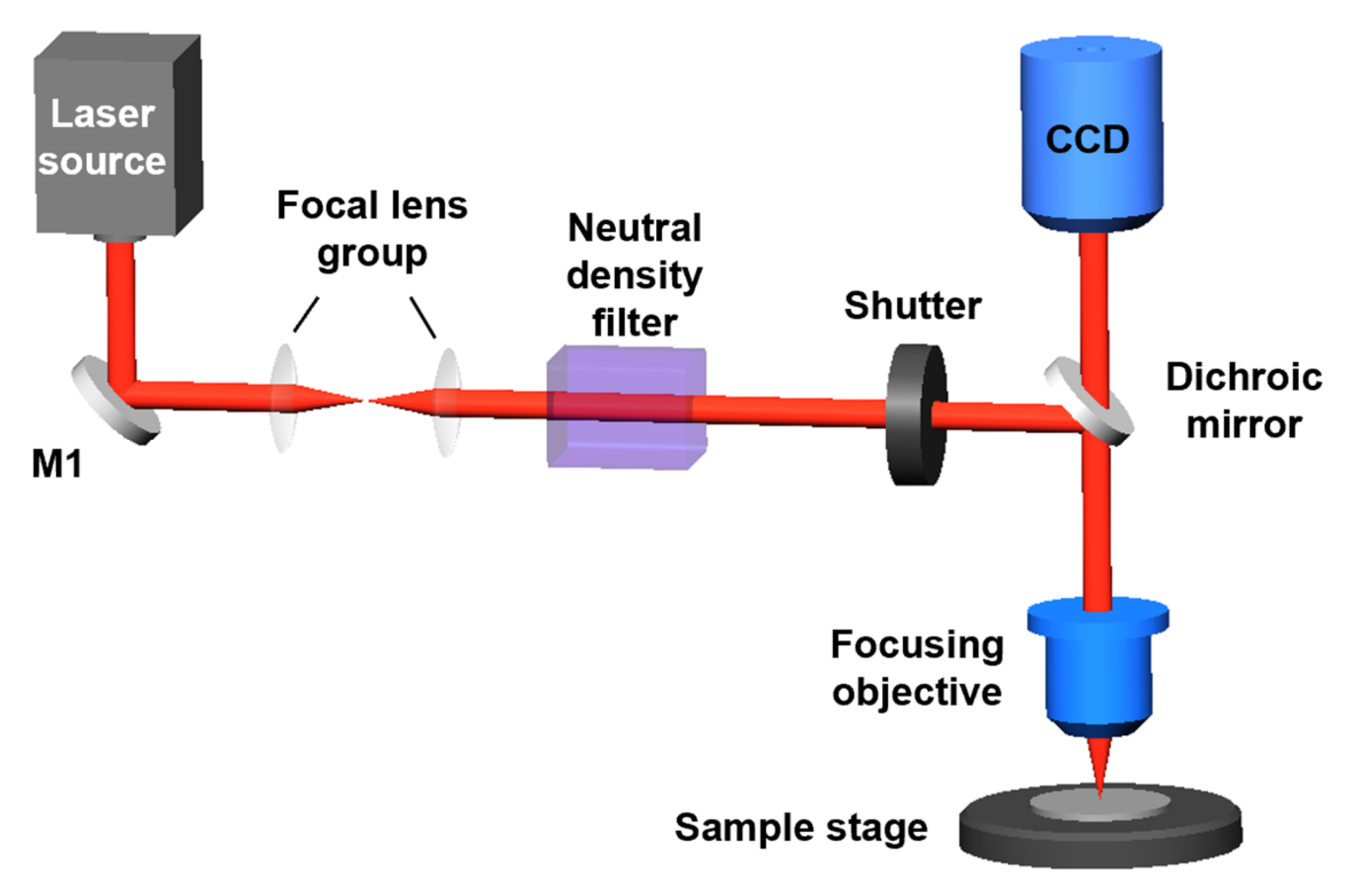
2. Experimental Details

Figure 1 shows a diagram of the laser irradiation system. The sapphire pulse laser had a central wavelength of 800 nm, a repetition rate of 1 kHz, and a pulse length of 120 fs. The duration of the laser was controlled using an electronic shutter. A neutral-density filter in the light path was utilized to adjust the laser radiation energy. The laser beam was focused on a circular spot with a diameter of ≈5 μm and perpendicular to the sample’s surface. The samples were placed on a precise XY translation stage. The range of the pulse energies used in this experiment was set from 20 to 50 nJ, corresponding to laser fluences from 1.02 to 2.55 J/cm2. All the laser ablation experiments were performed in an air environment under normal incidence. A crystal <100> n-type silicon wafer was selected as the semiconductor material for the laser-induced experiment for the reason that n-type crystalline silicon with patterned surface structures used in crystalline silicon solar cells show higher bulk quality and greater stability [30,31]. A Bi-In film with a thickness of 195 nm was deposited on silicon using electron beam evaporation (EBE). After laser ablation, the irradiated regions were characterized by scanning electron microscopy (SEM) and atomic force microscopy (AFM).

3. Results and Discussions

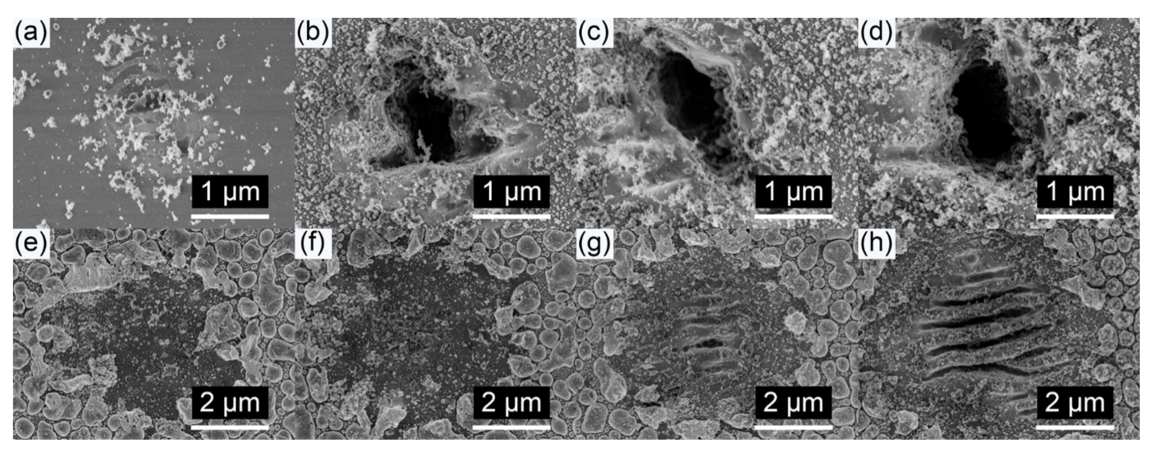
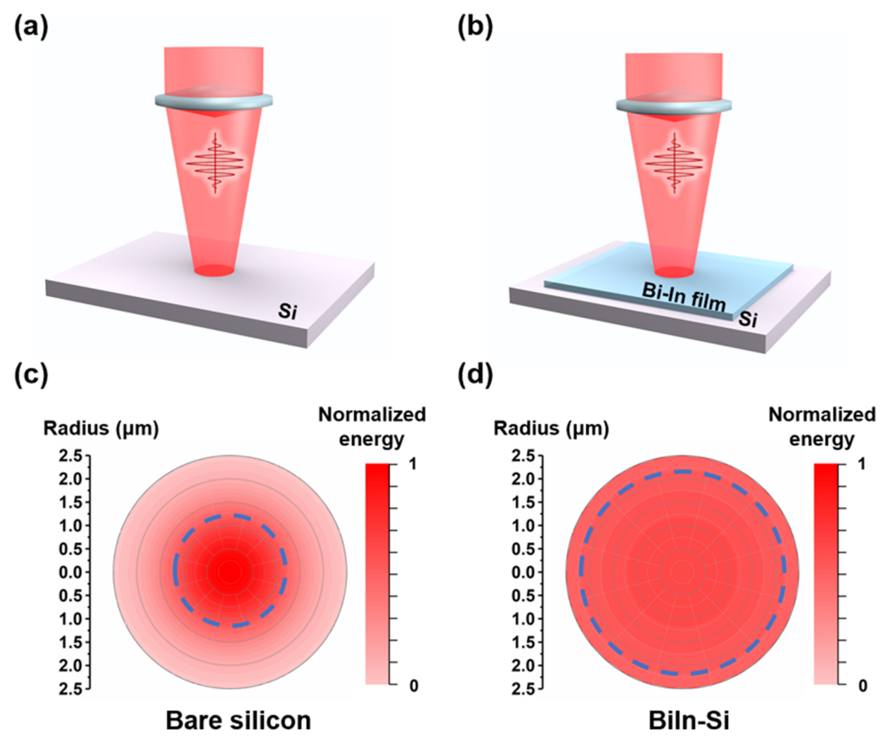
3.1. Single-Spot Investigations on Silicon and BiIn-Si

Generally, a single-spot investigation is required to obtain a detailed analysis of the effect of laser fluence on the formation process before the line-like or area-like generation of LIPSSs. Consequently, bare silicon and silicon coated with a Bi-In film (BiIn-Si) were irradiated with different laser fluences. Figure 2 shows the SEM images of the LIPSSs on bare silicon and BiIn-Si under laser fluences varying from 1.02 to 2.55 J/cm2 with a fixed laser pulse number N = 200. At the laser fluence of 1.02 J/cm2 (Figure 2a), surface modification occurred and the obtained structures were not well-defined grating structures. However, when irradiated with higher laser fluences (Figure 2b–d), the bare silicon surfaces were damaged due to the excessive energy. For silicon with a pre-deposited Bi-In film, as shown in Figure 2e, the alloy film on the silicon was removed with only a laser fluence of 1.02 J/cm2. When the laser fluence F = 1.53 J/cm2, ablation appeared on the silicon surface (Figure 2f). Grating structures started to be generated on the silicon surface at the laser fluence of 2.04 J/cm2 (Figure 2g). Better-defined ripple structures with an orientation perpendicular to the laser beam polarization were generated as the laser fluence was further increased to 2.55 J/cm2 (Figure 2h). As shown in Figure 2, high-quality periodic ripple structures were hard to generate on bare silicon when the laser energy varied from 20 to 50 nJ with a small interval of 10 nJ. However, distinct ripple structures were formed on BiIn-Si at the laser fluences of 2.04 and 2.55 J/cm2 due to the excellent thermal conductivity contributed by free electrons in the Bi-In film that allowed for avoiding energy localization. Moreover, the Bi-In film enabled a wider range of laser fluences to generate periodic structures, providing higher stability for fabrication.

3.2. Assistance Effect of Bi-In Alloy Film

Based on the above analysis, the optimal laser fluences that could form structures on bare silicon and BiIn-Si were 1.02 and 2.55 J/cm2, respectively. To analyze the assistance effect of the Bi-In film accurately, modified surface morphologies with different scanning speeds were observed on bare silicon (Figure 3a–c) and on BiIn-Si (Figure 3d–f) at their respective optimal laser fluences. For bare silicon, the ripple structures were irregular. For example, at a scanning speed of 40 μm/s (Figure 3b), the ripples were sharp in the middle and blurred at the edge. At a higher speed (Figure 3c), the ripples were discontinuous due to the discontinuity of the laser energy caused by the high scanning speed. In Figure 3d–f, for comparison, well-defined and distinct ripples were induced on BiIn-Si. The LIPSSs on BiIn-Si were more uniform with clear ridges and grooves, indicating that the Bi-In film contributed to the formation of uniform LIPSSs.
The mechanism of the nanolayered Bi-In alloy film that assisted with the femtosecond laser fabrication of uniform periodic surface structures is discussed as follows. The formation of LIPSSs on the silicon surface is explained by the interference between the incident laser radiation and the SPP wave. The period of the LIPSSs is expressed as [32]:
LIPSS   =   λ s = λ ε 1 + ε 2 ε 1 ε 2 1 / 2 =   λ 1 ε 1 + 1 ε 2 1 / 2 ,
where ∆LIPSS is the period of the ripples, λ is the wavelength of the laser, λs is the wavelength of the surface plasmon polariton wave, and ε1 and ε2 are the dielectric constants of the adjoining media. In our experiments, ε1 and ε2 represent the dielectric constants of air and Si, respectively. ε2 is defined as:
ε 2 = 1 ω p 2 ω 2 ,
where ωpne1/2, and ne is the free electron density. According to the above analysis, the period of the ripples is equal to the wavelength of the SPP wave. As the laser fluence increases, the free electron density of the plasma layer will increase, resulting in a decrease in ε2. Consequently, the period of ripples will increase. The surface morphologies of the ripple structures are affected by the energy distribution of the laser. As shown in Figure 4a, when the bare silicon was irradiated by the laser, the laser energy was mainly concentrated in the center of the spot according to the Gaussian distribution of the laser energy (Figure 4c), which caused the ripples to be clearer or even damaged at the center of the laser spot and blurry or nonexistent at the edge of the laser spot. This analysis agrees with our experimental results in Figure 3b. However, with the assistance of the Bi-In film, which contains massive free electrons, the electrons excited by the incident laser pulse can transport thermal energy quickly due to their high heat conduction performance. The thermal conductivity of Bi-In alloy contributed by the electrons can be calculated as 8.9 W/(m∙K) at 110 °C [33,34]. When the Bi-In film still existed on the silicon, the laser energy distribution in the laser spot on silicon was nearly uniform, as seen in Figure 4d. The circular blue dashed lines indicate the threshold of the laser fluence that led to the formation of ripple structures. Thus, the modified area on BiIn-Si was larger than that on bare silicon, which coincides with the results in Figure 3, where the width of the modified area was ≈2 μm on bare silicon (Figure 3a–c) and ≈4.5 μm on BiIn-Si (Figure 3d–f). Furthermore, the uniform distribution of laser energy meant that there was localized ablation on silicon. After a few pulses of irradiation, the Bi-In film was nonexistent, where the latter LIPSSs evolved along the original uniform grating structure direction due to the effect of the grating-assisted surface plasmon (SP)–laser coupling [24,35]. As a result, inhomogeneity in the energy distribution was reduced in the early stage of formation of the ripple structures, then the initial grating assisted in the formation of the latter uniform ripple structures.

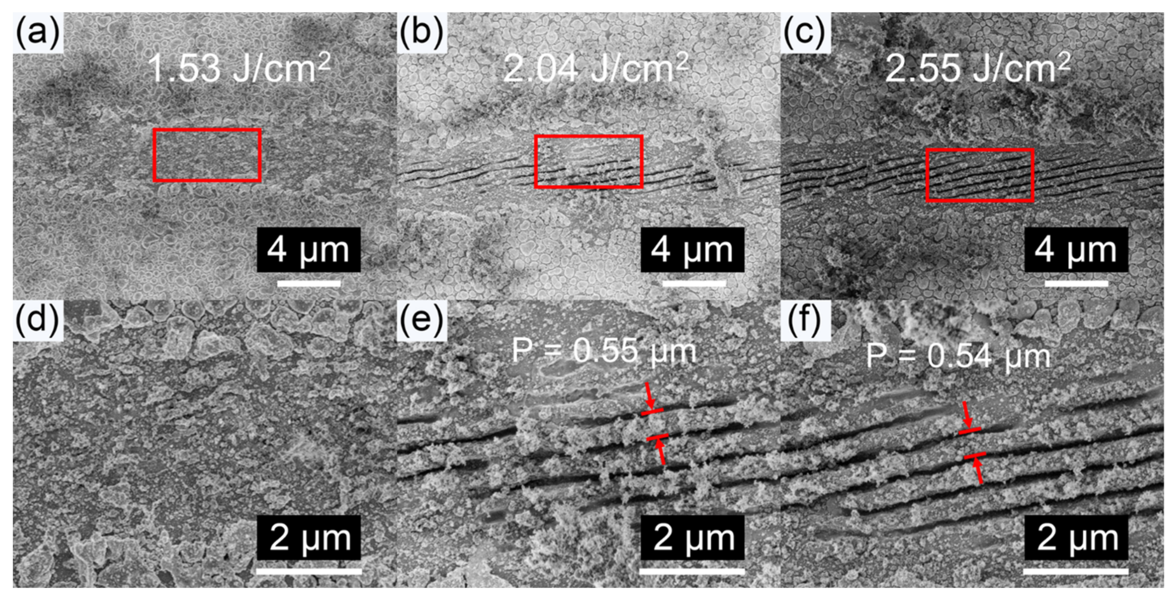
3.3. Effect of Laser Fluence on the Fabrication of Nanostructures on BiIn-Si

To study the tuning effects of the laser parameters on ripple structures, experiments on the laser fluence and the pulse number dependences of surface structures were performed. The effect of the laser fluence on the period of the ripple structures is discussed first. Figure 5 shows the irradiated areas on the surface of BiIn-Si with laser fluences in the range from 1.53 to 2.55 J/cm2 at a scan speed of 20 μm/s. As shown in Figure 5a, no ripple was formed due to there being insufficient energy. With the laser fluence increased to 2.04 J/cm2, ripple structures were generated (Figure 5b) and the period of ripples was 0.55 μm, as seen in Figure 5e. When the laser fluence reached 2.55 J/cm2, the period of the ripples was 0.54 μm, which almost remained unchanged. The results indicate that the free electron density of the plasma layer was almost the same at two different laser fluences, which could be deduced from the mechanism discussed above. The possible reason for this phenomenon is that strong reflection, even up to a reflectivity of 60%, may have occurred at the early stage of ablation with a higher laser fluence [36]. Thus, the excitations of free electrons by the laser fluences of 2.04 J/cm2 (Figure 5b) and 2.55 J/cm2 (Figure 5c) were equivalent [37], with no obvious change observed in the ripple period.

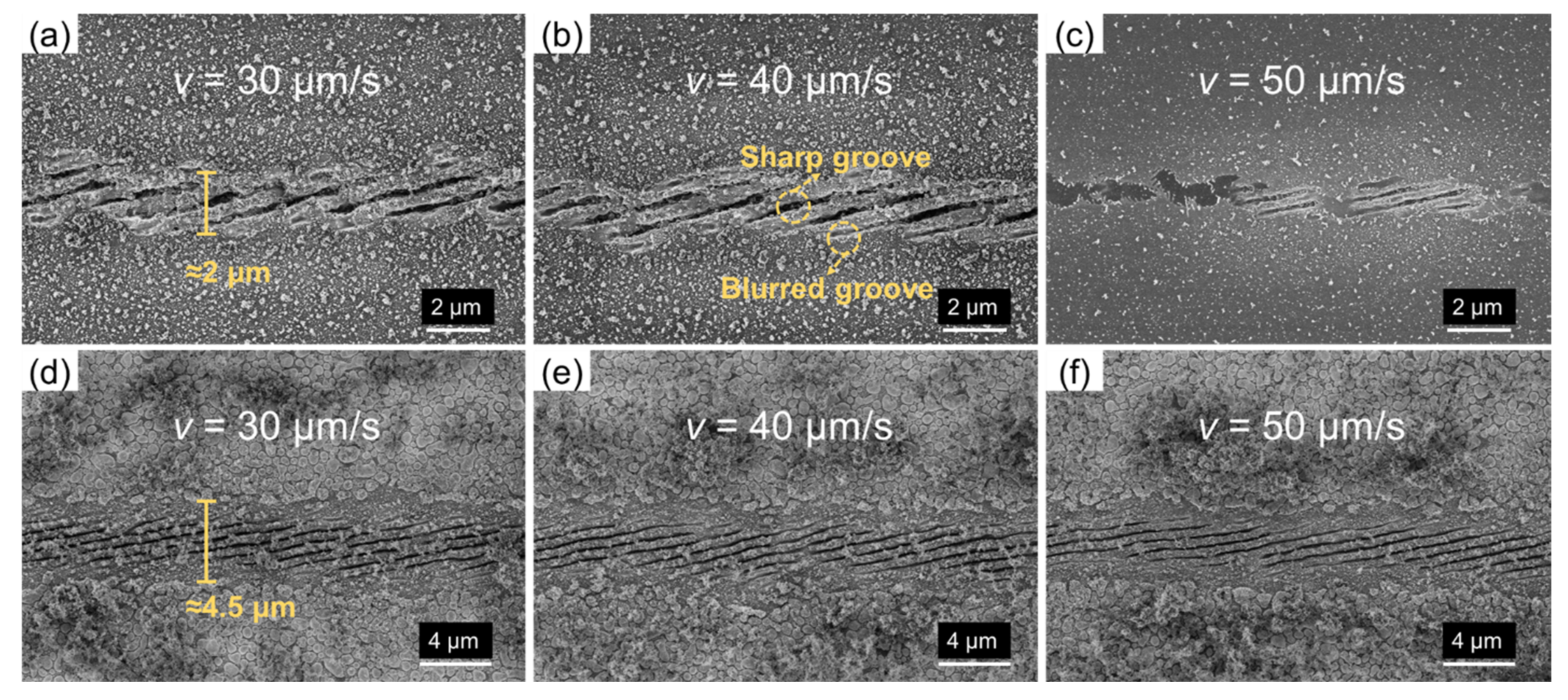
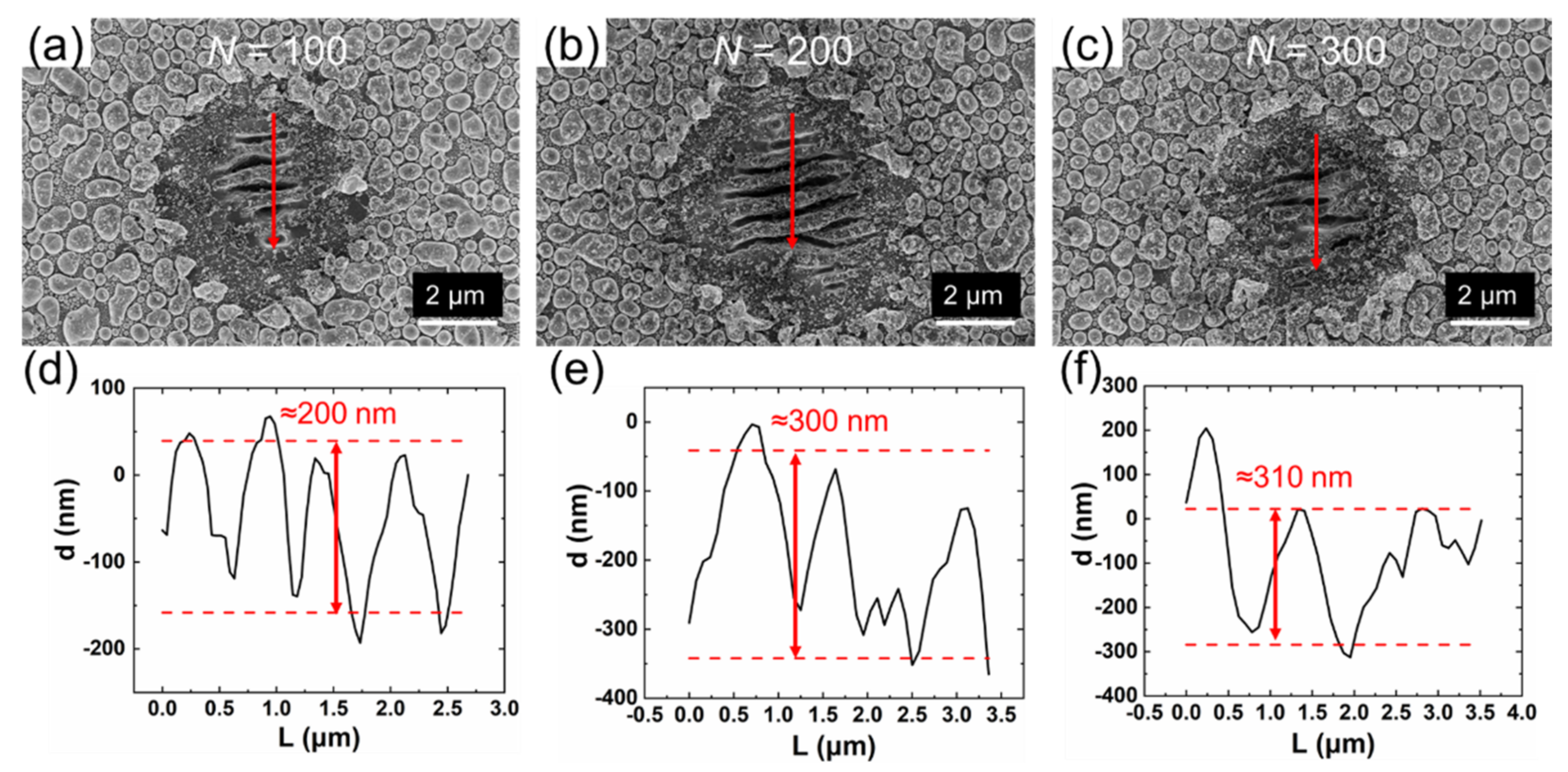
3.4. Effect of the Laser Pulse Number on the Fabrication of Nanostructures on BiIn-Si

Figure 6 depicts the laser pulse number effect on the ripple structures. The laser fluence of the femtosecond laser was maintained at 2.55 J/cm2. At a laser pulse number of 100, ripple structures were formed (Figure 6a), and a depth of ≈200 nm was obtained from the AFM image (Figure 6d). With the laser pulse number increasing to 200, the ripple structures became distinct (Figure 6b), with the depth reaching ≈300 nm (Figure 6e). When the pulse number was N = 300 (Figure 6c), the periodic structures were distorted due to heat accumulation [38]. Figure 6d,e shows that the depth of the ripple structures increased when the laser pulse number increased from 100 to 200. Nevertheless, when the laser pulse number was increased to 300, the depth did not increase because the ripple structures were damaged. The results indicate that the depth could be modulated by changing the number of laser pulses. However, the accumulated thermal energy must be less than the damage threshold.

4. Conclusions

In summary, an approach for obtaining uniform LIPSSs on silicon using a pre-deposited Bi-In thin film was proposed in this work. The effects of the Bi-In film were analyzed both theoretically and experimentally. The Bi-In film acted as a buffer layer to homogenize the distribution of thermal energy caused by laser irradiation and avoid damaging the silicon due to excess heat in the formation of the initial LIPSSs. Then, the grating-assisted SP–laser coupling further assisted the formation of LIPSSs. We also investigated the tuning effects of laser parameters (laser fluence and pulse number) on the ripple structures. With the laser fluences varying from 1.02 to 2.55 J/cm2 at a scanning speed of 20 μm/s, no obvious change in the ripple period was observed due to the reflection enhancement. Furthermore, the depth of the ripples could be modulated by the laser pulse number. Nevertheless, periodic structures may be distorted by heat accumulation. This approach opens new opportunities for obtaining high-quality periodic structures on easily damaged materials.

Author Contributions

Writing—original draft preparation, Y.C.; writing—review and editing, Y.S., H.T., H.Z., R.H., Y.Z., R.Z., S.W., J.L., and L.C.; supervision, Y.Z. All authors have read and agreed to the published version of the manuscript.

Funding

This research was funded by the National Natural Science Foundation of China (61775042, 61427815, 11674062) and the Fudan University-CIOMP Joint Fund (FC2017-003).

Institutional Review Board Statement

Not applicable.

Informed Consent Statement

Not applicable.

Data Availability Statement

Data are contained within the herein article.

Conflicts of Interest

The authors declare no conflict of interest.

References

  1. Birnbaum, M. Semiconductor Surface Damage Produced by Ruby Lasers. J. Appl. Phys. 1965, 36, 3688–3689. [Google Scholar] [CrossRef]
  2. Höhm, S.; Rosenfeld, A.; Krüger, J.; Bonse, J. Femtosecond laser-induced periodic surface structures on silica. J. Appl. Phys. 2012, 112, 014901. [Google Scholar] [CrossRef]
  3. Van Driel, H.M.; Sipe, J.E.; Young, J.F. Laser-Induced Periodic Surface Structure on Solids: A Universal Phenomenon. Phys. Rev. Lett. 1982, 49, 1955–1958. [Google Scholar] [CrossRef]
  4. Wang, C.; Luo, Z.; Duan, J.; Jiang, L.; Sun, X.; Hu, Y.; Zhou, J.; Lu, Y. Adjustable annular rings of periodic surface structures induced by spatially shaped femtosecond laser. Laser Phys. Lett. 2015, 12, 056001. [Google Scholar] [CrossRef]
  5. Shi, X.; Xu, X. Laser fluence dependence of ripple formation on fused silica by femtosecond laser irradiation. Appl. Phys. A 2019, 125, 256. [Google Scholar] [CrossRef]
  6. Bonse, J.; Krüger, J. Pulse number dependence of laser-induced periodic surface structures for femtosecond laser irradiation of silicon. J. Appl. Phys. 2010, 108, 034903. [Google Scholar] [CrossRef]
  7. Gräf, S.; Müller, F.A. Polarisation-dependent generation of fs-laser induced periodic surface structures. Appl. Surf. Sci. 2015, 331, 150–155. [Google Scholar] [CrossRef]
  8. Gregorčič, P.; Sedlaček, M.; Podgornik, B.; Reif, J. Formation of laser-induced periodic surface structures (LIPSS) on tool steel by multiple picosecond laser pulses of different polarizations. Appl. Surf. Sci. 2016, 387, 698–706. [Google Scholar] [CrossRef] [Green Version]
  9. Albu, C.; Dinescu, A.; Filipescu, M.; Ulmeanu, M.; Zamfirescu, M. Periodical structures induced by femtosecond laser on metals in air and liquid environments. Appl. Surf. Sci. 2013, 278, 347–351. [Google Scholar] [CrossRef]
  10. Trtica, M.; Stasic, J.; Batani, D.; Benocci, R.; Narayanan, V.; Ciganovic, J. Laser-assisted surface modification of Ti-implant in air and water environment. Appl. Surf. Sci. 2018, 428, 669–675. [Google Scholar] [CrossRef]
  11. Vorobyev, A.Y.; Guo, C. Femtosecond laser-induced periodic surface structure formation on tungsten. J. Appl. Phys. 2008, 104, 063523. [Google Scholar] [CrossRef]
  12. Reif, J.; Costache, F.; Henyk, M.; Pandelov, S.V. Ripples revisited: Non-classical morphology at the bottom of femtosecond laser ablation craters in transparent dielectrics. Appl. Surf. Sci. 2002, 197–198, 891–895. [Google Scholar] [CrossRef]
  13. Shimotsuma, Y.; Kazansky, P.G.; Qiu, J.; Hirao, K. Self-Organized Nanogratings in Glass Irradiated by Ultrashort Light Pulses. Phys. Rev. Lett. 2003, 91, 247405. [Google Scholar] [CrossRef] [PubMed] [Green Version]
  14. Miyaji, G.; Miyazaki, K.; Zhang, K.; Yoshifuji, T.; Fujita, J. Mechanism of femtosecond-laser-induced periodic nanostructure formation on crystalline silicon surface immersed in water. Opt. Express 2012, 20, 14848–14856. [Google Scholar] [CrossRef]
  15. Garrelie, F.; Colombier, J.P.; Pigeon, F.; Tonchev, S.; Faure, N.; Bounhalli, M.; Reynaud, S.; Parriaux, O. Evidence of surface plasmon resonance in ultrafast laser-induced ripples. Opt. Express 2011, 19, 9035–9043. [Google Scholar] [CrossRef]
  16. Yang, Y.; Yang, J.; Xue, L.; Guo, Y. Surface patterning on periodicity of femtosecond laser-induced ripples. Appl. Phys. Lett. 2010, 97, 141101. [Google Scholar] [CrossRef]
  17. Bonse, J.; Rosenfeld, A.; Krüger, J. On the role of surface plasmon polaritons in the formation of laser-induced periodic surface structures upon irradiation of silicon by femtosecond-laser pulses. J. Appl. Phys. 2009, 106, 104910. [Google Scholar] [CrossRef]
  18. Vorobyev, A.Y.; Guo, C. Antireflection effect of femtosecond laser-induced periodic surface structures on silicon. Opt. Express 2011, 19, A1031–A1036. [Google Scholar] [CrossRef]
  19. Al-Kattan, A.; Ali, L.M.A.; Daurat, M.; Mattana, E.; Gary-Bobo, M. Biological Assessment of Laser-Synthesized Silicon Nanoparticles Effect in Two-Photon Photodynamic Therapy on Breast Cancer MCF-7 Cells. Nanomaterials 2020, 10, 1462. [Google Scholar] [CrossRef]
  20. Ebert, T.; Neumann, N.W.; Döhl, L.N.K.; Jarrett, J.; Baird, C.; Heathcote, R.; Hesse, M.; Hughes, A.; McKenna, P.; Neely, D.; et al. Enhanced brightness of a laser-driven x-ray and particle source by microstructured surfaces of silicon targets. Phys. Plasmas 2020, 27, 043106. [Google Scholar] [CrossRef]
  21. Mangaiyarkarasi, D.; Sheng, O.Y.; Breese, M.B.H.; Fuh, V.L.S.; Xioasong, E.T. Fabrication of large-area patterned porous silicon distributed Bragg reflectors. Opt. Express 2008, 16, 12757–12763. [Google Scholar] [CrossRef] [PubMed] [Green Version]
  22. Öktem, B.; Pavlov, I.; Ilday, S.; Kalaycıoğlu, H.; Rybak, A.; Yavaş, S.; Erdoğan, M.; Ilday, F.Ö. Nonlinear laser lithography for indefinitely large-area nanostructuring with femtosecond pulses. Nat. Photonics 2013, 7, 897–901. [Google Scholar] [CrossRef]
  23. Ardron, M.; Weston, N.; Hand, D. A practical technique for the generation of highly uniform LIPSS. Appl. Surf. Sci. 2014, 313, 123–131. [Google Scholar] [CrossRef] [Green Version]
  24. Feng, P.; Jiang, L.; Li, X.; Rong, W.; Zhang, K.; Cao, Q. Gold-film coating assisted femtosecond laser fabrication of large-area, uniform periodic surface structures. Appl. Opt. 2015, 54, 1314–1319. [Google Scholar] [CrossRef] [PubMed]
  25. Yang, H.Z.; Jiang, G.D.; Wang, W.J.; Mei, X.S.; Pan, A.F.; Zhai, Z.Y. Picosecond laser fabrication of nanostructures on ITO film surface assisted by pre-deposited Au film. Appl. Phys. B 2017, 123, 251. [Google Scholar] [CrossRef]
  26. Yin, K.; Wang, C.; Duan, J.; Guo, C. Femtosecond laser-induced periodic surface structural formation on sapphire with nanolayered gold coating. Appl. Phys. A 2016, 122, 834. [Google Scholar] [CrossRef]
  27. Jafari Eskandari, M.; Shafyei, A.; Razi, S.; Shoja Razavi, R. Influence of gold nanolayer coating on the continuous-wave laser ablation of a pure aluminum surface: Evaluations of structural and optical features. Thin Solid Film. 2019, 672, 126–132. [Google Scholar] [CrossRef]
  28. Kalantar-Zadeh, K.; Tang, J.; Daeneke, T.; O’Mullane, A.P.; Stewart, L.A.; Liu, J.; Majidi, C.; Ruoff, R.S.; Weiss, P.S.; Dickey, M.D. Emergence of Liquid Metals in Nanotechnology. ACS Nano 2019, 13, 7388–7395. [Google Scholar] [CrossRef]
  29. Daeneke, T.; Khoshmanesh, K.; Mahmood, N.; de Castro, I.A.; Esrafilzadeh, D.; Barrow, S.J.; Dickey, M.D.; Kalantar-zadeh, K. Liquid metals: Fundamentals and applications in chemistry. Chem. Soc. Rev. 2018, 47, 4073–4111. [Google Scholar] [CrossRef]
  30. Wang, W.; He, J.; Yan, D.; Samundsett, C.; Phang, S.P.; Huang, Z.; Shen, W.; Bullock, J.; Wan, Y. 21.3%-efficient n-type silicon solar cell with a full area rear TiOx/LiF/Al electron-selective contact. Sol. Energy Mater. Sol. Cells 2020, 206, 110291. [Google Scholar] [CrossRef]
  31. Wan, Y.; Samundsett, C.; Yan, D.; Allen, T.; Peng, J.; Cui, J.; Zhang, X.; Bullock, J.; Cuevas, A. A magnesium/amorphous silicon passivating contact for n-type crystalline silicon solar cells. Appl. Phys. Lett. 2016, 109, 113901. [Google Scholar] [CrossRef] [Green Version]
  32. Alexey, M.B.-B.; Mikhail, N.L.; Vladimir, S.M.; Vladimir, V.T. Surface electromagnetic waves in optics. Opt. Eng. 1992, 31, 718–730. [Google Scholar]
  33. Makinson, R.E.B. The thermal conductivity of metals. Math. Proc. Camb. Philos. Soc. 1938, 34, 474–497. [Google Scholar] [CrossRef]
  34. Ohno, S.; Tamaki, S. Electronic properties of liquid In-Bi alloys. J. Phys. Soc. Jpn. 1975, 38, 538–543. [Google Scholar] [CrossRef]
  35. Huang, M.; Zhao, F.; Cheng, Y.; Xu, N.; Xu, Z. Origin of Laser-Induced Near-Subwavelength Ripples: Interference between Surface Plasmons and Incident Laser. ACS Nano 2009, 3, 4062–4070. [Google Scholar] [CrossRef]
  36. Von der Linde, D.; Schüler, H. Breakdown threshold and plasma formation in femtosecond laser–solid interaction. J. Opt. Soc. Am. B 1996, 13, 216–222. [Google Scholar] [CrossRef]
  37. Han, Y.; Qu, S. The ripples and nanoparticles on silicon irradiated by femtosecond laser. Chem. Phys. Lett. 2010, 495, 241–244. [Google Scholar] [CrossRef]
  38. Liao, Y.; Pan, W.; Cui, Y.; Qiao, L.; Bellouard, Y.; Sugioka, K.; Cheng, Y. Formation of in-volume nanogratings with sub-100-nm periods in glass by femtosecond laser irradiation. Opt. Lett. 2015, 40, 3623–3626. [Google Scholar] [CrossRef] [Green Version]
Figure 1. Schematic diagram of the experimental setup for the generation of laser-induced periodic surface structures (LIPSSs). CCD: charge-coupled device.
Applsci 11 00632 g001
Figure 2. Scanning electron microscopy (SEM) images of the surface morphologies on bare silicon and BiIn-Si with different laser fluences of (a,e) 1.02, (b,f) 1.53, (c,g) 2.04, and (d,h) 2.55 J/cm2 at a fixed laser pulse number of N = 200. (ad) represent situations on bare silicon. (eh) represent situations on BiIn-Si.
Applsci 11 00632 g002
Figure 3. SEM images of the surface morphologies written on samples. (ac) correspond to morphologies of bare silicon with different scanning speeds at a fixed laser fluence of 1.02 J/cm2. (df) correspond to morphologies of BiIn-Si with different scanning speeds at a fixed laser fluence of 2.55 J/cm2. The scanning speeds were 30, 40, and 50 μm/s, as labeled on the images.
Applsci 11 00632 g003
Figure 4. Schematic diagrams of the laser irradiation on samples. The laser beam was incident on the bare silicon (a) and on BiIn-Si (b). A sketch diagram of the energy distribution on bare silicon (c) and BiIn-Si (d).
Applsci 11 00632 g004
Figure 5. SEM images of the surface morphologies with a scan speed of 20 μm/s on BiIn-Si. (df) are the magnified versions of the areas within the red rectangles of (ac), respectively. P is the period of the ripples.
Applsci 11 00632 g005
Figure 6. SEM images and AFM profiles of the surface morphologies fabricated on BiIn-Si at a fixed laser fluence of 2.55 J/cm2. (ac) correspond to SEM images and (df) correspond to AFM profiles with different scanning speeds. N is laser pulse number.
Applsci 11 00632 g006
Publisher’s Note: MDPI stays neutral with regard to jurisdictional claims in published maps and institutional affiliations.

