1. Introduction
Logic synthesis aimed at minimizing power consumption is currently one of the most important problems in the design of energy-saving digital circuits. One of the most popular families of digital circuits is the very complex programmable Systems on Chips using LUT-based FPGAs. Until recently, the goal of optimizing the synthesis process was to minimize the number of LUTs or to minimize the length of the so-called critical path affecting the maximum clock frequency. Along with technological development, the problem of heat dissipation began to play a dominant role; thus, resulting in the need to reduce power consumption. The development of mobile devices is also important, as it forces the necessity to minimize energy consumption.
Minimizing power consumption should be sought at every level of circuit design. The stage of the system synthesis, at which the greatest limitations of power consumption can be found, undoubtedly depends on the specificity of the designed system. The greatest benefits are to be expected when looking for a reduction in power losses at the highest design levels [
1]. The decision to divide the task into software and hardware parts can have a significant impact on energy efficiency [
2]. Only at the highest design level is it also possible to anticipate the temporary shutdown of the modules of the designed hardware and software system, which undoubtedly significantly reduces the total power of losses. Many concepts of power minimization at the system level can be found in [
3,
4,
5,
6]. They are often related to the problems of high-level synthesis, presented, inter alia, in [
7,
8,
9,
10].
However, the power savings at lower synthesis levels are also important. From the point of view of saving power consumption, the most advantageous techniques are minimization techniques aimed at minimizing both static and dynamic power consumption. Such a concept of reducing power consumption are undoubtedly the methods of local lowering the supply voltage [
11,
12], or recently very popular methods called “power gating” [
10,
11,
12,
13,
14]. However, they cannot be used in FPGAs. Methods aimed at minimizing dynamic power consumption, with particular emphasis on automatic logical synthesis algorithms, are also of great importance in the minimization process. Most of them are related to the methods of limiting the power consumption of synchronous systems. The essence of many methods of synthesizing energy-saving circuits comes down to minimizing the switching. Among them, there are various techniques for limiting the frequency of the clock signal. Sometimes it is possible to reduce the frequency of the global clock signal, but this leads to a longer execution of individual functions, which often adversely affects the operation of the entire system. In this situation, the possibility of temporarily blocking the clock signal (clock gating) [
15] is often sought. The possibility of blocking the clock signal can be predicted by analyzing the state of the input signals. There are many architectural concepts known for the possibility of blocking the clock signal. Among them, for example, it is worth distinguishing the precomputation logic method [
16], the kernel extraction method [
17,
18,
19], or various FSM decomposition methods [
20,
21].
Much more sophisticated solutions are related to the local lowering of the clock signal frequency, which are possible to be implemented in less loaded modules of a complex digital system. In this case, however, there is a problem with the synchronization of data exchange in two modules working with different clock signals. A very interesting concept of reducing power losses is the implementation of systems in the form of a GALS (globally asynchronous locally synchronous) structure, which makes it possible to adjust the frequency of the local clock signal to the computational needs of a given unit, but requires the use of asynchronous interface blocks enabling data exchange. Solutions of this type work well in complex systems in which the modules are not evenly loaded with the performed calculations [
22]. It should be emphasized that methods of limiting power consumption begin to play a key role in low-level synthesis. Appropriately carried out selected synthesis steps can lead to a reduction in power consumption by programmable systems. This is especially visible in the case of the implementation of FSMs [
23,
24,
25]. There are several ways to reduce power consumption when implementing FSM. The methods associated with the appropriate FSM internal state coding [
26] are very promising. Moreover, in the case of combinational systems, there are methods that enable a reduction in power consumption, as shown in the works of [
27,
28,
29,
30,
31].
The aim of this article is to present a low-level method of logical synthesis leading to a reduction in power consumption by combinational circuits implemented in FPGAs. This method is directly related to the function decomposition and technological mapping in LUT-based FPGAs. Appropriate modification of the decomposition leads to the creation of a new synthesis strategy aimed at minimizing the power consumption of the logical structure.
The first part of this article presents the theoretical basis of decomposition using the description of a function in the form of BDD (in its reduced ordered form ROBDD). Then, the essence of limiting power consumption by reducing switching activity is presented. In the next part of the article, a new form of the diagram is introduced—SWBDD—which allows the authors to propose an appropriate synthesis strategy aimed at minimizing dynamic power consumption. The next section contains a general description of the algorithm implemented in the PowerDekBDD tool, in which the ideas presented were implemented. The article ends with the section “Experimental Results,” presenting the effectiveness of the described strategy, and “Summary,” which contains conclusions and an indicated direction for further work.
2. Theoretical Background
One of the main tasks of logic synthesis geared toward FPGAs is to map the implemented logic structure into FPGA resources. The technology mapping in the case of combinational circuits comes down to the mapping of the implemented function from LUT logical blocks included in the circuit. It turns out that LUT logical blocks are capable of executing any logic function with a limited number of variables. The number of
k inputs of the LUT (number of function variables) is small. Therefore, there is a problem of dividing the implemented circuit. The mathematical model of such a division is the decomposition of a function. The decomposition theorem was formulated by Ashenhurst [
32] and developed by Curtis [
33] as early as the 1960s. In the classical approach, simple serial decomposition comes down to splitting all variables into two sets: bound set
Xb and free set
Xf. The variables contained in the bound set are variables for the bound functions
g [
33], which are implemented in the bound block. On the other hand, the bound functions and the variables from the free set are variables of the free function realized in the free block. From the point of view of efficient partitioning, the key is the number of bound functions
p, which corresponds to the number of wires between the bound and free blocks.
Let f be n-input and m-output logic function reflecting Bn set into Bm set i.e., f: Bn → Bm, where B = {0, 1}. Function f: Bn → Bm may be presented as Y = f(In−1, …, I1, I0), where Y = {ym−1, ..., y1, y0}.
Function f:
Bn →
Bm is subjected to decomposition, i.e.,
if and only if column multiplicity of Karnaugh map
[
32,
33], where
Xb ∪
Xf = {
In−1, …,
I1,
I0} and
.
Simple serial decomposition leads to the division shown in
Figure 1.
The method of describing a function plays a key role in the decomposition process, which determines the computational complexity of individual operations and memory usage. It turns out that in this respect, the representation of the function in the form of BDD [
34,
35,
36] is very effective. Of course, there are many different forms of BDD. In this paper, the authors refer to the reduced and ordered form of BDD (ROBDD) when using the term BDD.
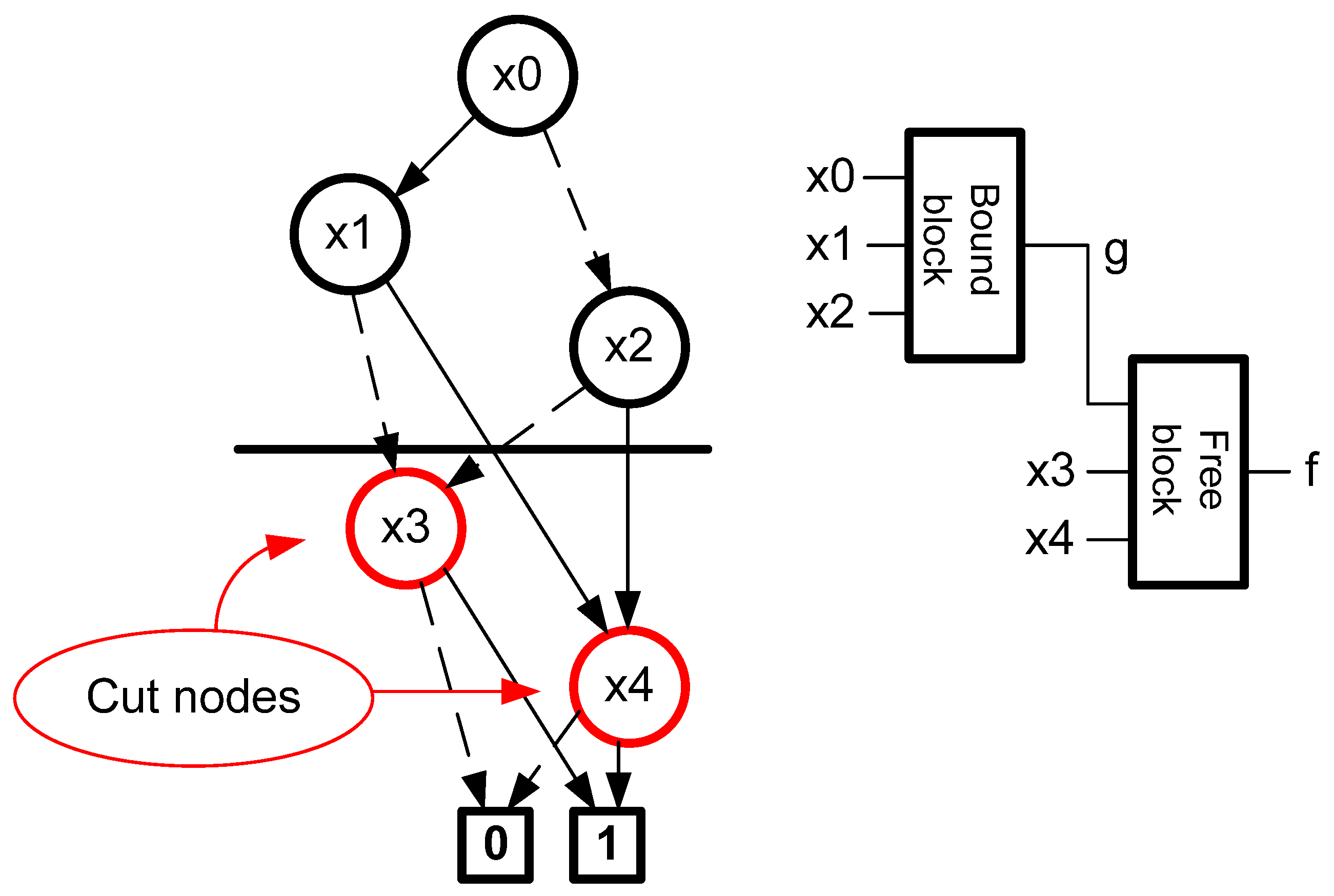
The essence of BDD decomposition is to cut the diagram horizontally. This divides the nodes into those above the cut line and the nodes below the cut line. The variables associated with the top of the diagram belong to the bound set
Xb. On the other hand, the variables associated with the bottom of the diagram belong to the free set
Xf. In the case of BDD, column multiplicity corresponds to the number of cut nodes. Cut nodes are the nodes at the bottom of the diagram (below the cut line) to which the edges above the cut line are drawn. The essence of the implementation of decomposition with the use of BDD is shown in
Figure 2.
There are also some modifications to the presented method. As shown in the works [
37,
38], the decomposition can also be realized by introducing several cut lines for one BDD. Simple serial decomposition is the basis for more complex decomposition models, such as multiple or iterative decomposition, which can also be realized with the use of BDD [
39,
40].
In order to obtain efficient decomposition, the aim is to limit the number of bound functions, which allows the complexity of the bound block to be reduced. It is, therefore, necessary to limit the number of cut nodes. It turns out that the number of cut nodes depends on two factors: the level of BDD cut and the order of variables in the diagram. The cut level determines the cardinality of the bound set
card(Xb). This value corresponds to the number of inputs in LUT block (
k). Thus, the cut level is assumed to be k from the root of the BDD
(card(Xb) = k). The number of cut nodes at a given level depends on the order of the variables. Therefore, it is necessary to analyze many orderings of variables. The idea of a quick reordering in BDD in terms of decomposition was presented in [
41].
As the search for the best decomposition is an iterative process, it is necessary to estimate the effectiveness of the divisions obtained each time. As a rule, the number of LUT block inputs is somewhat configurable, which complicates the process. One of the solutions to this problem is the use of triangle tables [
42]. Assuming that the number of inputs is not configurable, instead of determining the technology mapping coefficient from triangle tables, only the cost of implementing the considered decomposition for a constant value of k can be determined.
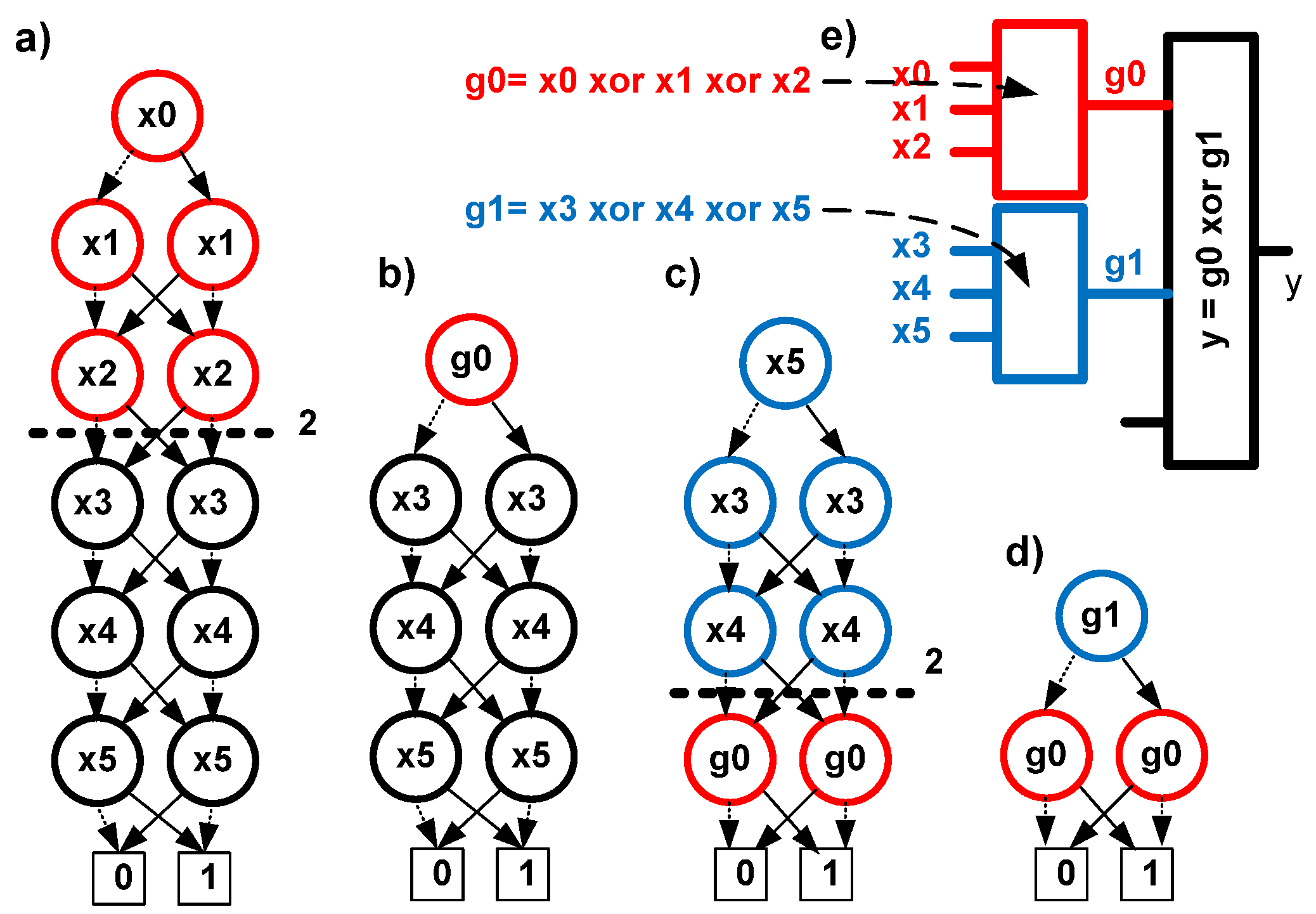
An example of technology mapping in LUT blocks with three inputs is shown in
Figure 3. The xor function described in BDD from
Figure 3a was decomposed by a single cut at level 3 from the root. Two cut nodes were obtained, which indicates the necessity to use a single bound function g0. In
Figure 3b, the top of the diagram is replaced with a single node associated with the newly created bound function (g0 = x0 xor x1 xor x2). The first step of decomposition ends with reordering the variables, leading to the diagram shown in
Figure 3c. In the second step of decomposition, the entire procedure is repeated, replacing the top of the diagram with a single node associated with g1 (g1 = x3 xor x4 xor x5). As a result, the diagram shown in
Figure 3d is created, describing the free function (y = g0 xor g1). After implementation in LUT blocks with three inputs, a structure is created as in
Figure 3e, the model of which is multiple decomposition.
3. A Synthesis Method Aimed at Minimizing Power Consumption
Power in digital systems can be divided into static power
Pstat and dynamic power
Pdyn (2):
The static power
Pstat depends on the technology of making the digital circuit. This power depends on many factors such as: gate leakage, drain junction leakage, sub-threshold current, i.e., a number of technological parameters. In the case of FPGAs, the designer has minimal possibilities to limit static power consumption in the process of designing the implemented circuit. It can only look for an FPGA chip that will ensure minimal static power consumption. In the case of dynamic power
Pdyn, the designer has a much greater impact on reducing power dissipation. The dynamic power is expressed with the relationship (3):
It is clearly visible that dynamic power depends on a number of factors. The main factor that allows the dynamic power to be limited is to reduce the supply voltage Vdd. Unfortunately, it is practically impossible to limit the supply voltage in FPGAs. Another factor influencing the dynamic power is the frequency of the clock signal f. Naturally, it is possible to imagine a local decrease in the clock frequency, although it should be remembered that, as a rule, the aim is to design structures as fast as possible, which means that this method usually cannot be used. The implemented logic structure resulting from decomposition is usually a logic network composed in the general case of n nodes. In the case of FPGAs, the nodes of this network correspond to the LUTs. The internal capacity Ci can be associated with the lines corresponding to the connections between the nodes of the network. This capacity must be reloaded each time in the process of switching logic states, which, of course, has an impact on dynamic power consumption. The value of the capacitance Ci can be treated individually due to the same technology of making the entire FPGA matrix. Therefore, it becomes crucial to determine how often this capacity is reloaded, i.e., the state changes to the opposite one in the i-th node. It is determined by introducing an additional SWi parameter into Formula (3), i.e., switching activity for each node. Thus, it can be concluded that limiting the switching activity for as many nodes of the logic network as possible should lead to the limitation of dynamic power dissipation. Thus, the idea of limiting switching activity appears at the stage of designing the implemented structure. However, a problem arises as to how to take into account the limitations of SW in low-level stages of synthesis, such as decomposition or technological mapping. In order to solve this problem, it becomes necessary to develop an appropriate form of description of a logic function, taking into account the parameter expressions in the description.
3.1. Switching Activity
Switching activity determines the probability of changing the state of the considered variable from the value 0 to the value 1 or from the value 1 to the value 0, which is related to the reload of the capacity Ci. Thus, the value of SW can be represented by the Formula (4):
where
P is the probability of the value 1 (or 0) occurring for the considered logic network node at a given time instant. It turns out that the expression (4) can be reduced if, as
P(x), we denote the probability of accepting the value 1 by the variable x and all inputs are mutually independent and uncorrelated in time, then the expression (4) can be reduced to the form (5):
In this situation, the expression (1 − P(x)) is the probability of the value 0. From the perspective of the function variables, it is very difficult to determine the probability value of the value 1. It is difficult to say whether 1 or 0 will occur on the selected input of the combinational circuit and with what probability. In this situation, it is necessary to make certain assumptions as to the probability of the value 1 (most often it is assumed that P(x = 0) = P(x = 1) = 0.5).
The relationship (5) shows that the probability of the occurrence of the value 1 in a given network node is related to its switching activity. The highest switching activity occurs for nodes for which the probability of occurrence of the value 1 is 0.5. In the process of synthesizing logic circuits implemented in FPGAs aimed at minimizing power consumption, decomposition becomes necessary, which is the basis for dividing the designed circuit into a network of LUTs. Therefore, there is a need for an appropriate BDD cut that also depends on the SW.
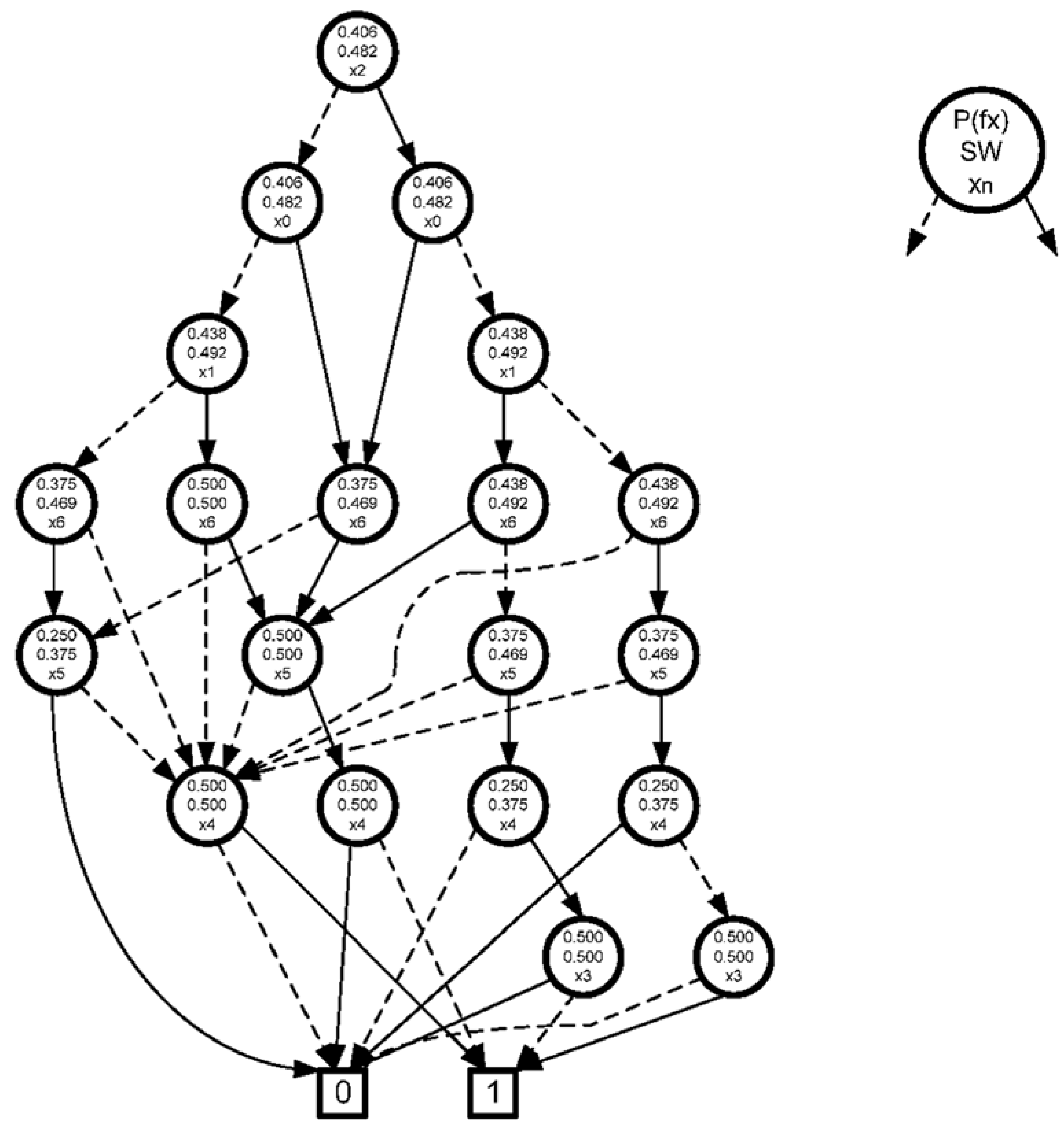
3.2. SWBDD—Switch Activity Binary Decision Diagram
In order to develop a synthesis strategy aimed at minimizing power dissipation, it is necessary to introduce a new diagram form—SWBDD. The new form of the diagram differs from the classic form of BDD (ROBDD) in that additional information has been placed in each node. In a single node, in addition to the information with which the variable is associated, there is also the value of the probability of one
P(fx) (to calculate which set of paths in the BDD leading to the leaf “1” will be used) and the SW value determined from the dependence (5) for the considered
P(fx). It should be emphasized that when analyzing the paths, it becomes necessary to determine the probability of the occurrence of the value 1 for individual variables. Assuming that the probabilities of the value 1 for all variables are the same and equal to 0.5, an exemplary SWBDD diagram is shown in
Figure 4.
Assuming the implementation of the function on LUT blocks, it becomes necessary to divide the diagram by cutting the diagram horizontally. It turns out that you can associate the value of the SW coefficient with the cut line equal to the sum of the SWi values associated with the vertices above the cut line. The value of this coefficient depends on the order of the nodes in the SWBDD.
3.3. Example
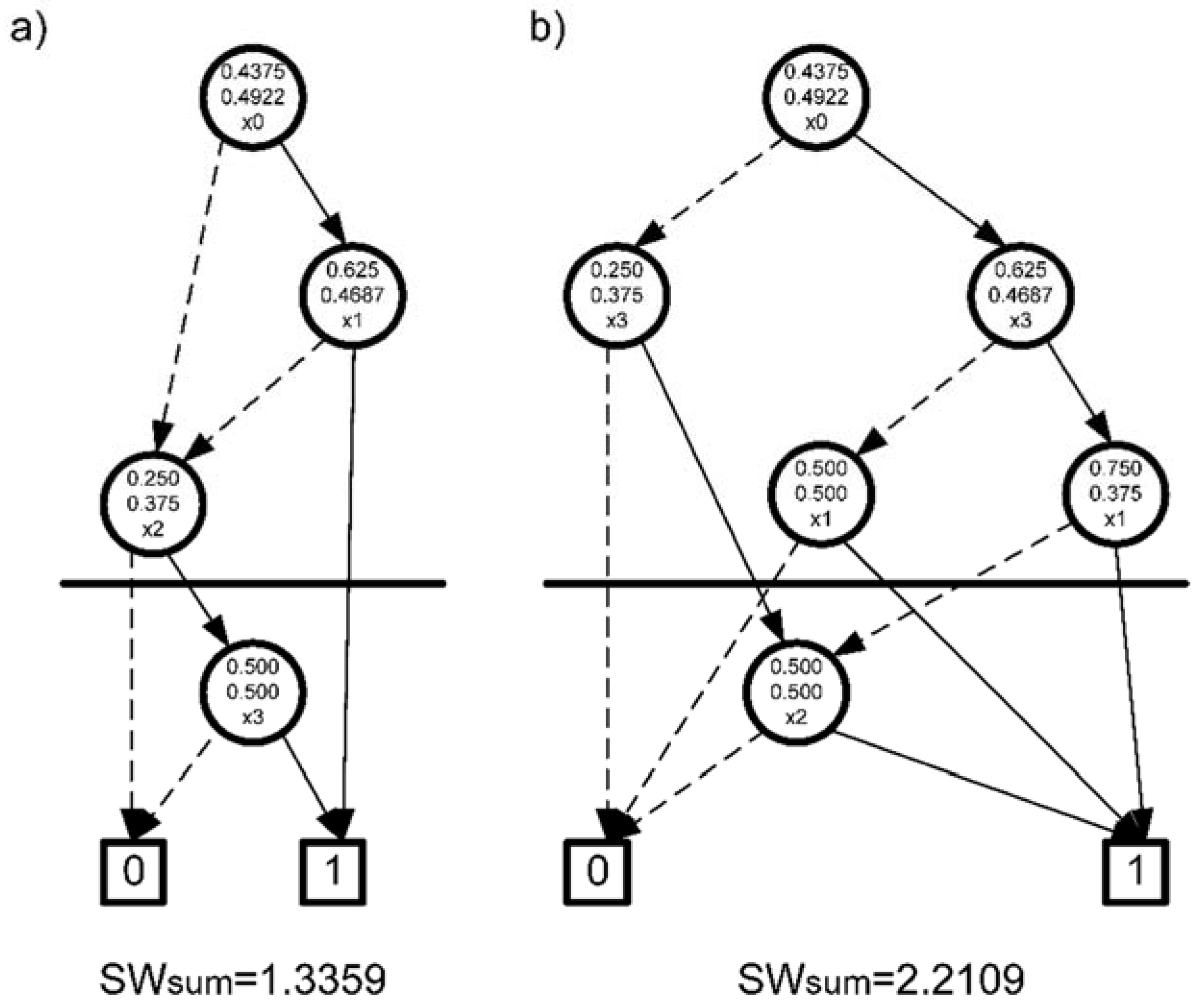
Consider the function
f(x0,
x1,
x2,
x3) described by SWBDD shown in
Figure 5. Let us assume that we want to implement it on LUT3/2 blocks (number of inputs/number of outputs). In this situation, it becomes necessary to intersect the SWBDD diagram in the place indicated in
Figure 5. In this case, the cardinality of the associated set is 3. For each diagram, the number of cut nodes is the same and includes the node associated with the corresponding variable below the cut line and two leaves. In this situation, in both cases, we need two LUT3/2 blocks to perform the function
f(x0,
x1,
x2,
x3). When looking at the SW coefficients associated with the nodes above the cut line of the two diagrams, they assume different values. It turns out that the value of the total coefficient for nodes above the cut line for the diagram in
Figure 5a is
SWsum = 1.3359 and is clearly smaller than the value of
SWsum for
Figure 5b (
SWsum = 2.2109). The sum value of the
SW coefficients associated with the nodes above the cut line should be used in the process of selecting the appropriate cut line for the SWBDD diagram.
4. The Strategy of Low Power Synthesis
As in the case of the classic form of BDD, the form of SWBDD can be used to perform decomposition using a horizontal cut line. As usual, the number of bound functions (
numb_of_g) and the cardinality of the bound set (
card(
Xb)) are key. Of course, as before, some optimization methods can be used, such as non-disjoint decomposition [
41,
42]. The essence of non-disjoint decomposition is to replace a number of bound functions with input variables, which leads to a reduction in the bound block. Naturally, these variables must meet certain conditions to be able to function as g functions. The number of replaced functions linking the variables x, for non-disjoint decomposition, will be given as
num_ndisj. It should be emphasized that a reduction in the number of LUTs achieved through non-disjoint decomposition is also beneficial in terms of power consumption reduction.
As in the case of the classic form of BDD, the process of finding the best decomposition in the case of SWBDD is also an iterative process, in which it is necessary to determine the value of the cost function for the implementation of a given cost decomposition. The use of SWBDD, thanks to the additional information contained in the nodes of the diagram, allows for the determination of additional parameters. Let bound_activity_sum (SWsum) be the cumulative SW value for all nodes above the cut line.
The performed numerous experiments allowed us to determine the cost function, which can be determined from the dependence (6)
The additional constants 32 and 128 were introduced only so that the multiplied part of the expression always has a greater effect on the cost value than the remainder. When analyzing the cost function, it can be observed that num_ndisj is always less than 32 and bound_activity_sum is always less than 128.
Including
SW in the function of decomposition cost causes the parameter associated with dynamic power to be added to the assessment of decomposition efficiency. In this situation, it is possible to propose an algorithm of a new synthesis strategy aimed at limiting the dynamic power consumption in the obtained solutions. The algorithm called PowerdekBDD is an extension of the dekBDD algorithm [
39,
40] known from the literature, which takes into account the element of minimizing dynamic power losses in the decomposition process.
Algorithm of Logic Decomposition Oriented to Power Optimization
The decomposition algorithm consists of the following steps repeated cyclically:
Search for the best bound set in a given step (lowest cost function value).
Create a g function for a bound block.
Create a function diagram with the top of the diagram (above the cut line) replaced by the variables g.
If there are still more variables in the diagram than the number of LUT inputs, go to step 1.
The key element during decomposition is finding the appropriate bound set (point 1). Since the bound set corresponds to the part above the cut line in the BDD diagram, searching for the appropriate bound set comes down to changing the order of variables in the diagram at a specific cut level. Checking all order combinations is very time-consuming and has a complexity of O(n!/(N − k)!). Such complexity is unacceptable in practical applications. In the proposed solution, thanks to the heuristic approach, the complexity was limited to O(k∗(n − k)). The pseudocode of the algorithm for searching for the best set of variables related to a given decomposition step is presented in Algorithm 1. The algorithm’s parameters are: F function diagram, k number of LUT block inputs, and n the number of function variables. The order of variables is changed in a double for loop (lines 5, 6). After changing the order of the variables xi and xj (line 7) for the obtained diagram, the cost is determined, allowing the quality of the obtained solution to be assessed.
In order to save computation time, the computation of the cost function was split into two steps: computing the cost related to the number of blockcost_Ftmp blocks (line 8) and computing activity_sum (line 10). The variable activity_sum is the summed activity values for functions rooted in nodes above the cut line. The calculation of activity_sum only takes place if blockcost_Ftmp does not have a greater value than the best solution found so far, thus saving processing time. If a better solution is found, it is remembered (line 13).
| Algorithm 1: The algorithm for searching for the best set of variables for bound set. |
FindBestBound(F)
2. //F function
3. //k number of LUT inputs
4. //n number of variables
5. for(i = 0; i < k; i++)
6. for(j = k; j < n; j++)
7. Ftmp= Swap(xi, xj, F) //swap variable order in BDD
8. blockcost_Ftmp= ((numb_of_g − card(Xb)) ∗ 32 + num_ndisj
9. if(blockcost_Ftmp is lower or equal than before)
10. activity_sum= CalculateBoundActivitySum();
11. totalcost_Ftmp= blockcost_Ftmp*128-activity_sum
12. if(totalcost_Ftmp is lower)
13. F = Ftmp |
5. Experimental Results
In order to test the effectiveness of the solutions obtained using the PowerDekBDD algorithm, a number of experiments were performed. The PowerDekBDD algorithm is implemented in the tool of the same name. A popular set of benchmarks [
43] was used for the experiments. Since Equation (6) does not take into account the sharing of logic resources between individual functions of the team, it was decided to consider each function separately and then sum the obtained results.
In the first series of experiments, it was decided to compare PowerDekBDD with other academic tools. Since PowerDekBDD is an extension of the DekBDD algorithm, it is crucial to compare both algorithms. Additionally, it was decided to compare with the leading synthesis tool ABC [
27]. The work [
44] discusses the appropriate scripts for the ABC system: “Baseline” as the basic one, and “PowerMap” and “PowerDC” as the scripts aimed at reducing power consumption. The comparisons between the tools were made, taking into account the necessary number of LUTs in the obtained “LUTs” solution (assumed k = 5) and the number of logic levels, “Levels,” obtained. Of course, additional information has also been added: in the case of the DekBDD and PowerDekBDD tools, the value of the achieved switching activity, “SW,” for each benchmark, while in the case of the ABC tool, the value of “Power” was given, which, as stated in [
44], is calculated on the basis of “SW.” According to the authors, the calculation methods of “Power” and “SW” in both tools are slightly different, and it is difficult to make a direct comparison between them. In order to maintain the reliability of the results, the authors provide the “Power” value for ABC, but at the same time emphasize that the purpose of compiling these results is not to compare them directly. The described list of results is presented in
Table 1.
The last rows of
Table 1 contain the sum value and the geometric sum. The values of the respective sums are summarized in the graphs in
Figure 6.
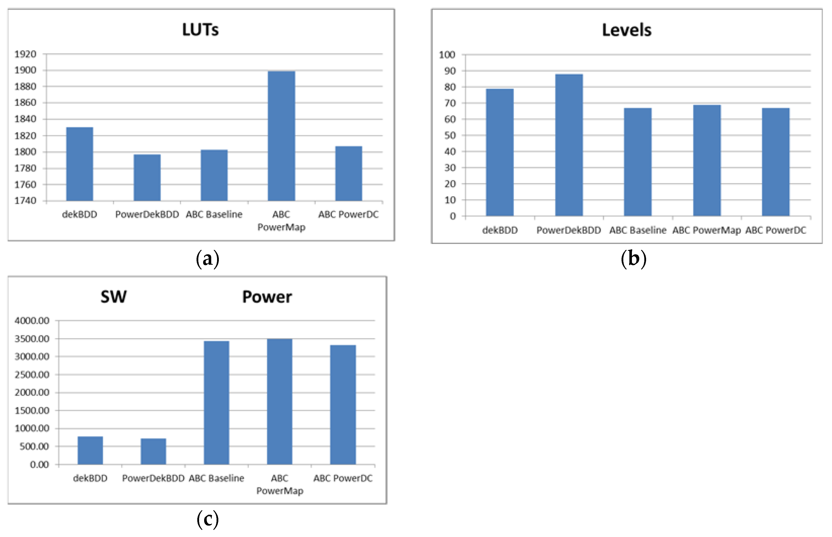
Analyzing the graph in
Figure 6a, it can be observed that the solutions obtained with the PowerDekBDD tool are the most effective in terms of the number of LUTs. The obtained improvement over DekBDD is about 2%. Taking into account
Figure 6b, it can be observed that the total number of logic levels for PowerDekBDD is slightly greater than for DekBDD. However, both solutions are much worse than the solutions obtained for ABC.
Figure 6c shows the comparison in terms of SW. In the case of PowerDekBDD, this parameter was reduced by over 5% compared with DekBDD. Unfortunately, it is impossible to reliably compare the PowerDekBDD method with the ABC system because the methodology of SW determination in both systems is slightly different; therefore, this issue will not be further developed.
Summarizing the comparison of academic systems, it can be stated that it was possible to reduce the number of blocks, but it is difficult to draw any conclusions as to the reduction in dynamic power dissipation (SW reduction), which is the main subject of this paper. In this situation, it was decided to conduct a second series of experiments, this time using a commercial tool from Xilinx–Vivado [
45].
The next steps of the synthesis in the Vivado system were performed with the default settings. The series 7 FPGA (Artix-7) was selected as the target device. The relevant results included in this paper were taken from the reports generated in this tool after the implementation process.
In the PowerDekBDD system, synthesized HDL (Verilog) descriptions of the function after decomposition were generated. Similarly, in ABC, similar descriptions were generated for the PowerDC script (PowerDC was selected due to the fact that the total value of “Power” was the lowest in
Table 1). It was decided to perform two series of experiments for PowerDC. In the first “PowerDC SF,” HDL descriptions of single functions (without sharing logical resources) obtained from ABC were further synthesized in Vivado. In the second “PowerDC MF,” descriptions of sets of functions were further synthesized. PowerDekBDD decomposes individual functions, but providing results for competing systems, including a set of functions, will, according to the authors, better define how the obtained solutions fit into the spectrum of other results. The obtained results are summarized in
Table 2. The individual columns in
Table 2, for each of the systems, describe: the number of “LUTs” blocks, the dynamic power consumed by the “Dynamic” implementation, and the dynamic power consumed only by the “LUT Power” LUTs.
The last rows of
Table 2 contain the sum value and the geometric sum. The values of the respective sums are summarized in the graphs in
Figure 7.
When analyzing the diagram in
Figure 7a, it can be observed that the solutions obtained for PowerDekBDD are very effective in terms of the number of blocks. The obtained results are much better than the results for PowerDC for single functions and practically the same as for the group of functions (thus taking into account resource sharing). Taking into account the overall dynamic power (graph in
Figure 7b), it can be observed that the obtained results are slightly worse than for PowerDC MF (which should be expected) and slightly better than for PowerDC (a reduction of 8% was achieved). A very similar situation occurs in the case of the diagram in
Figure 7c, showing the dynamic power consumed by the LUTs. In this case, it was possible to achieve a reduction of almost 24% compared with PowerDC SF. It should be emphasized, however, that in both cases, the values of the geometric mean were the same.
6. Conclusions
The new concept of the description of logic functions by means of SWBDD presented in the article is an interesting attempt to include in the process of automatic logic synthesis the issues of power dissipation minimization. It can be a form of description that allows for the minimization of power dissipation in the combination circuits described with the BDD. It can complement many synthesis methods in which BDD is used. This makes it possible to extend known synthesis methods without having to create new synthesis algorithms from scratch.
When analyzing the results of the experiments, it is clear that it is possible to develop a technology representation of the function in the form of a network of LUT blocks, in which there are the smallest possible losses related to the minimization of switching in individual nodes, directly related to the dynamic power dissipated in the circuit. The proposed algorithm is competitive in relation to alternative academic and commercial solutions. A significant weakness of the proposed solution is its limitation related to not taking into account the sharing of logical resources. In its current form, it is possible to analyze each function separately, which means that the obtained solutions can be definitely optimized. This type of optimization will become the basis for further work, the essence of which comes down to the optimization in terms of energy consumption of various synthesis strategies, in which various concepts of structure optimization, the use of a flexible configuration of LUTs, etc. play a leading role.


