
A New, Fast Pseudo-Random Pattern Generator for Advanced Logic Built-In Self-Test Structures


Abstract
:1. Introduction
2. Motivation
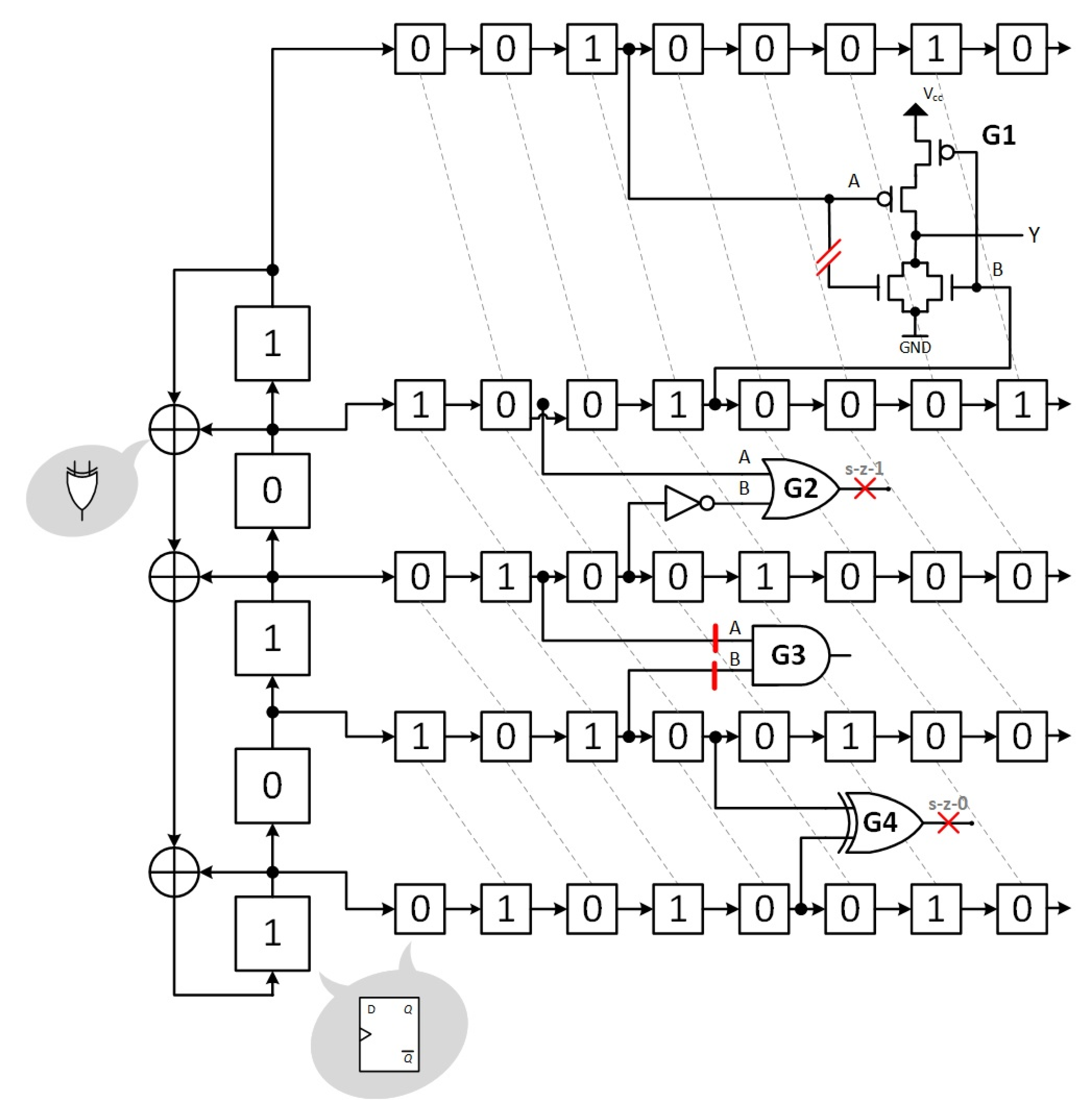
- Example 1
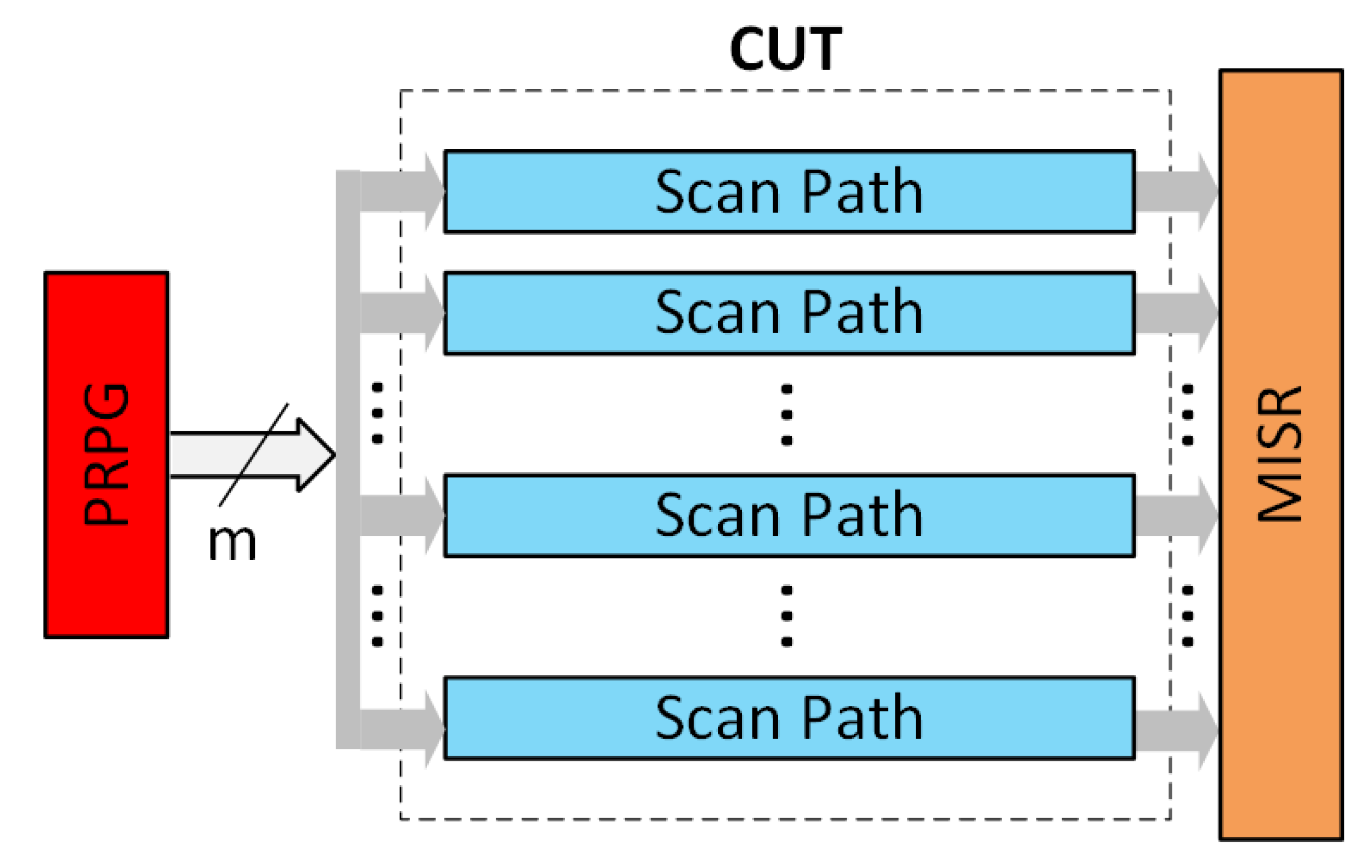
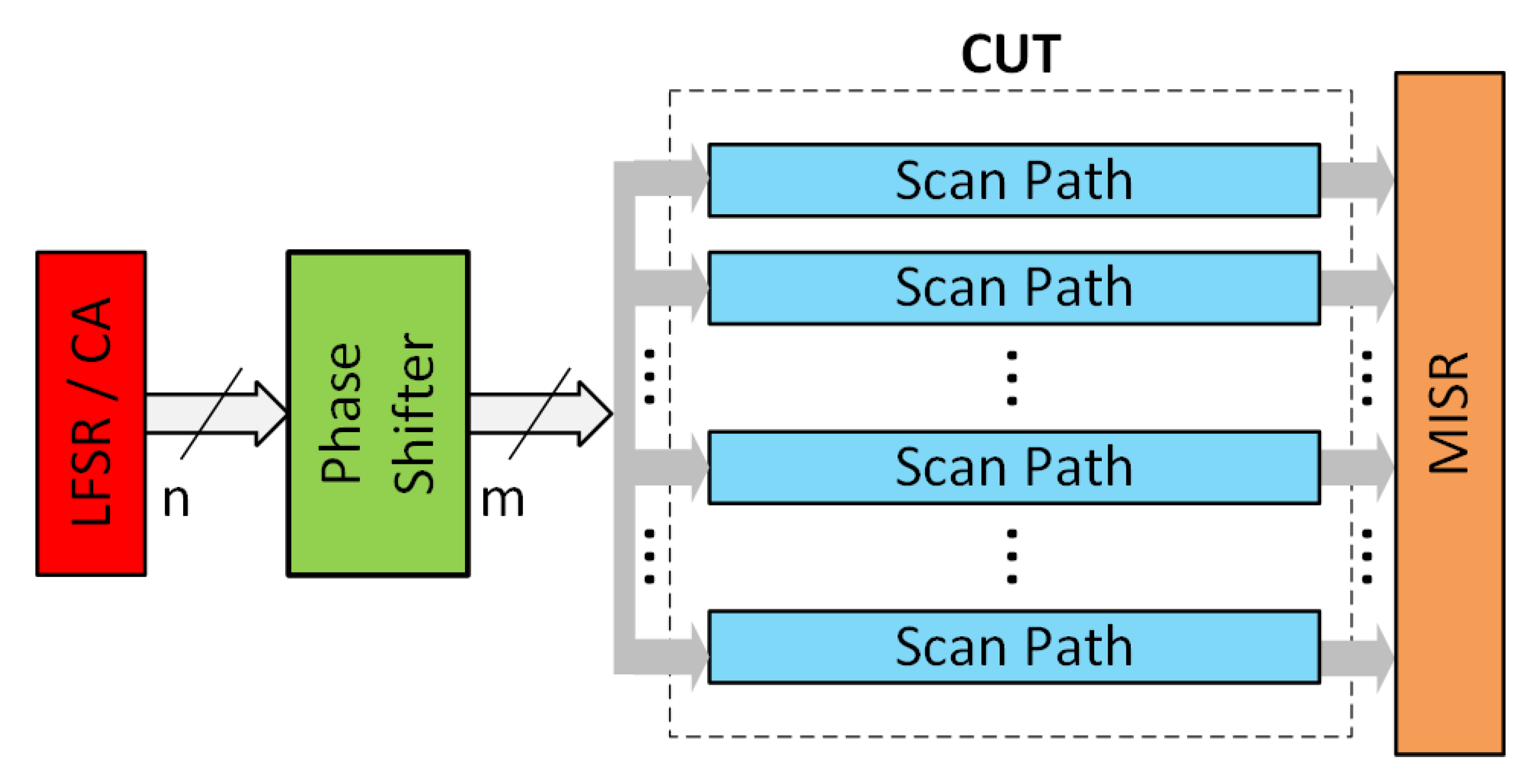
3. Classical Method to Design LBIST Circuits with the STUMPS Architecture
4. New Approach to Engineering of Pseudo-Random Pattern Generators for LBIST Circuits with the STUMPS Architecture
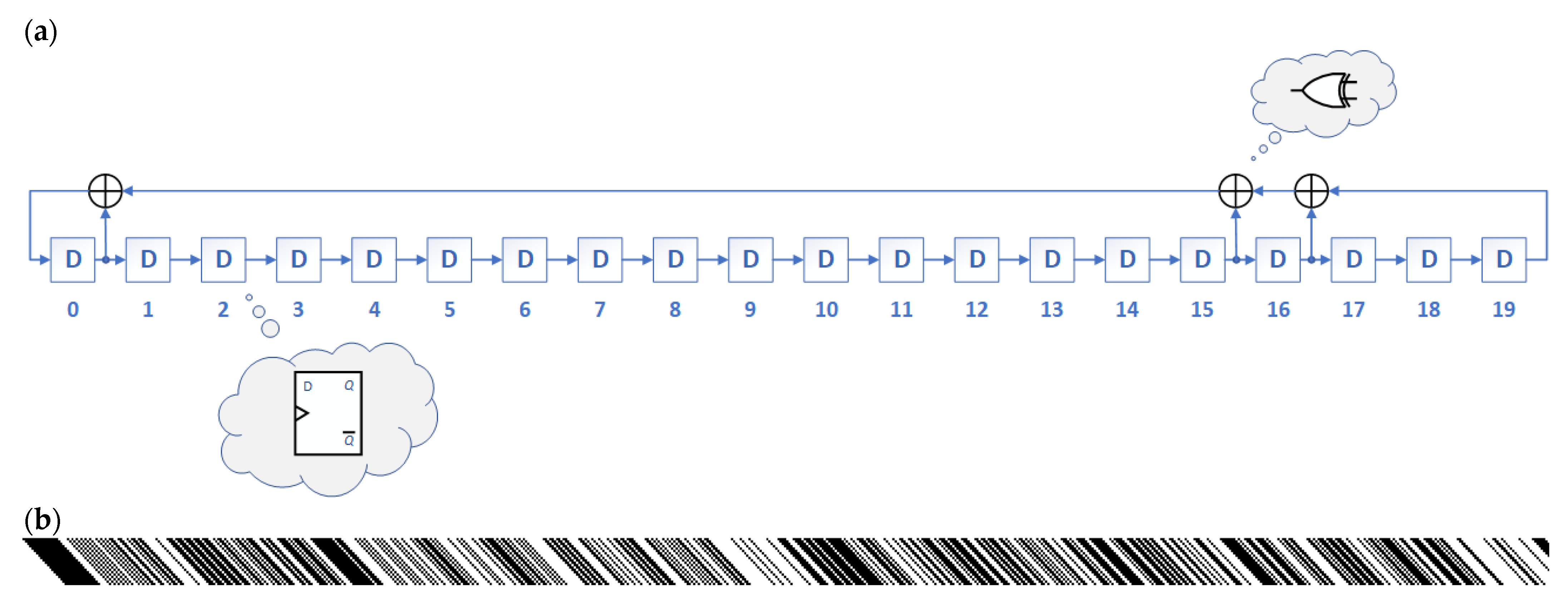
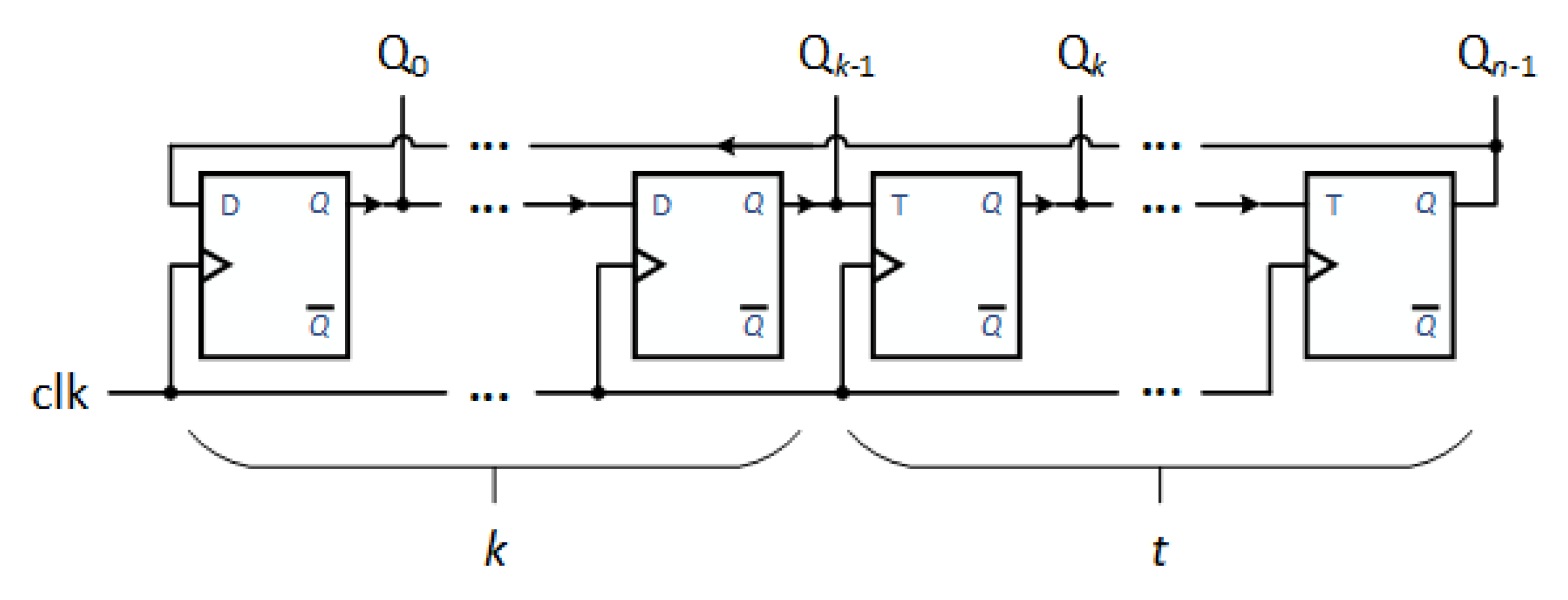
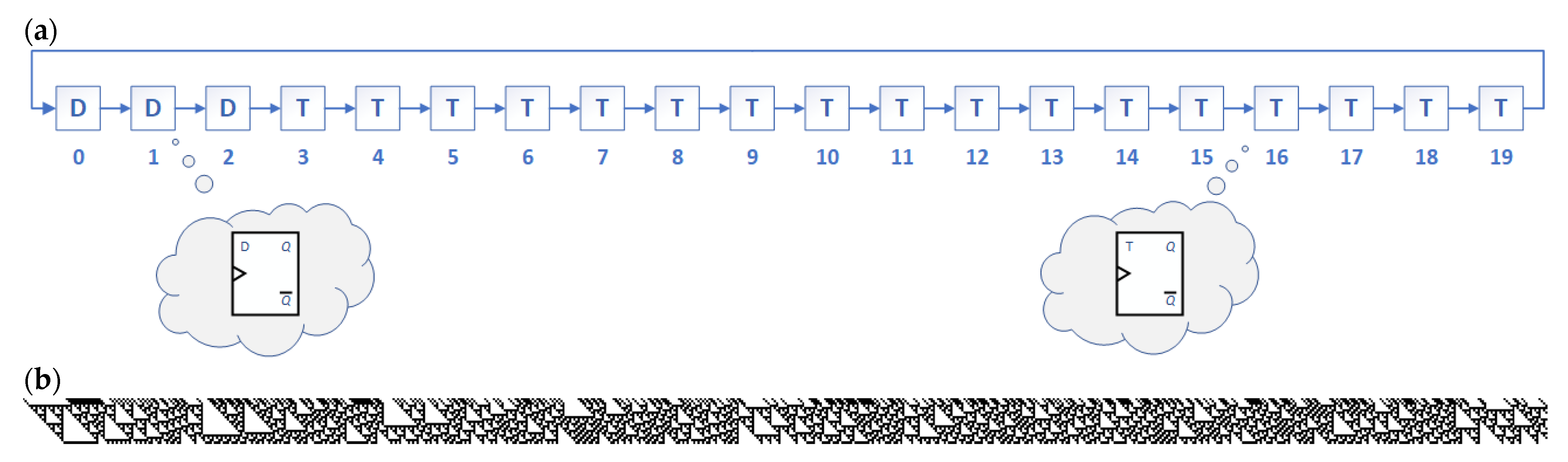
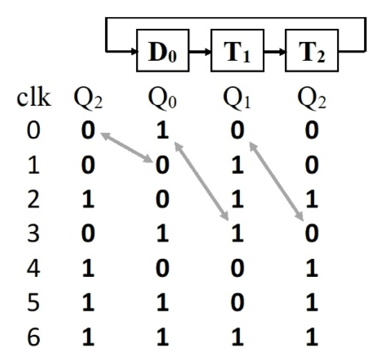
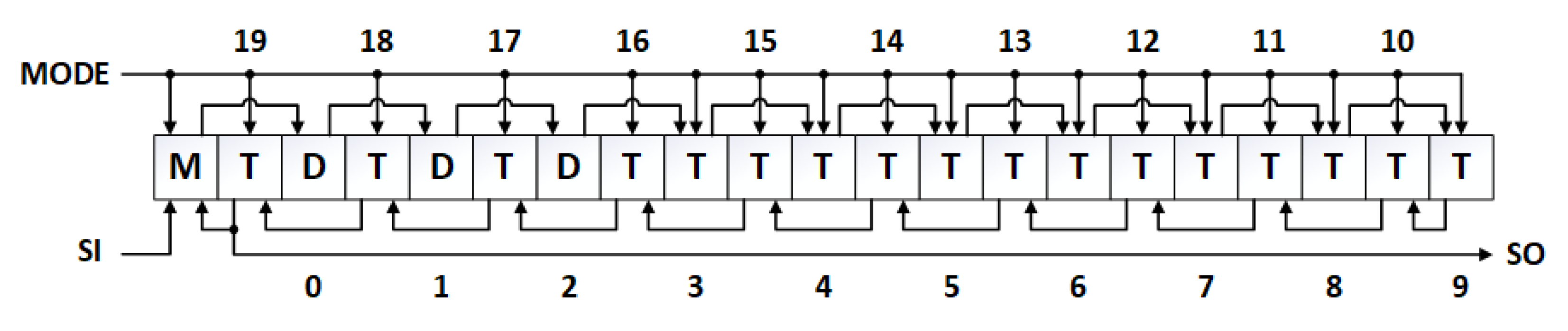
4.1. Layout of a DT-LFSR Register
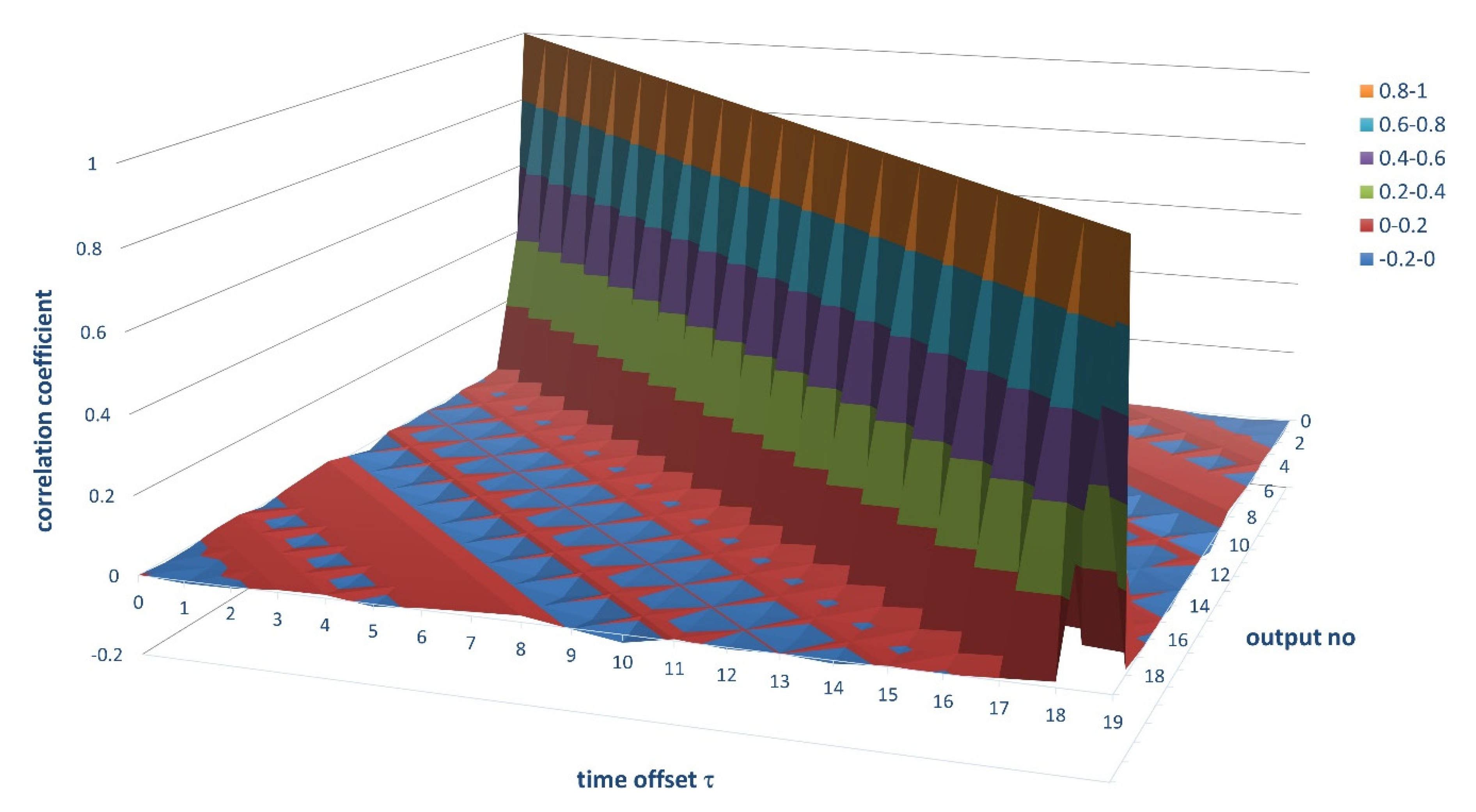
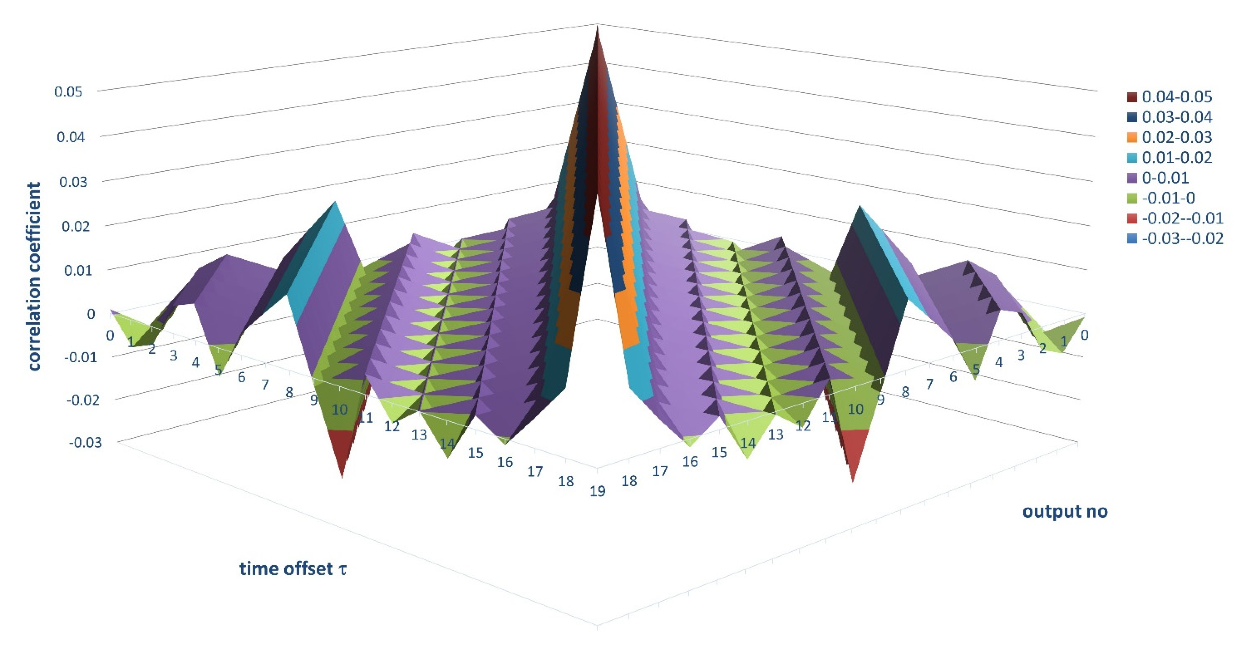
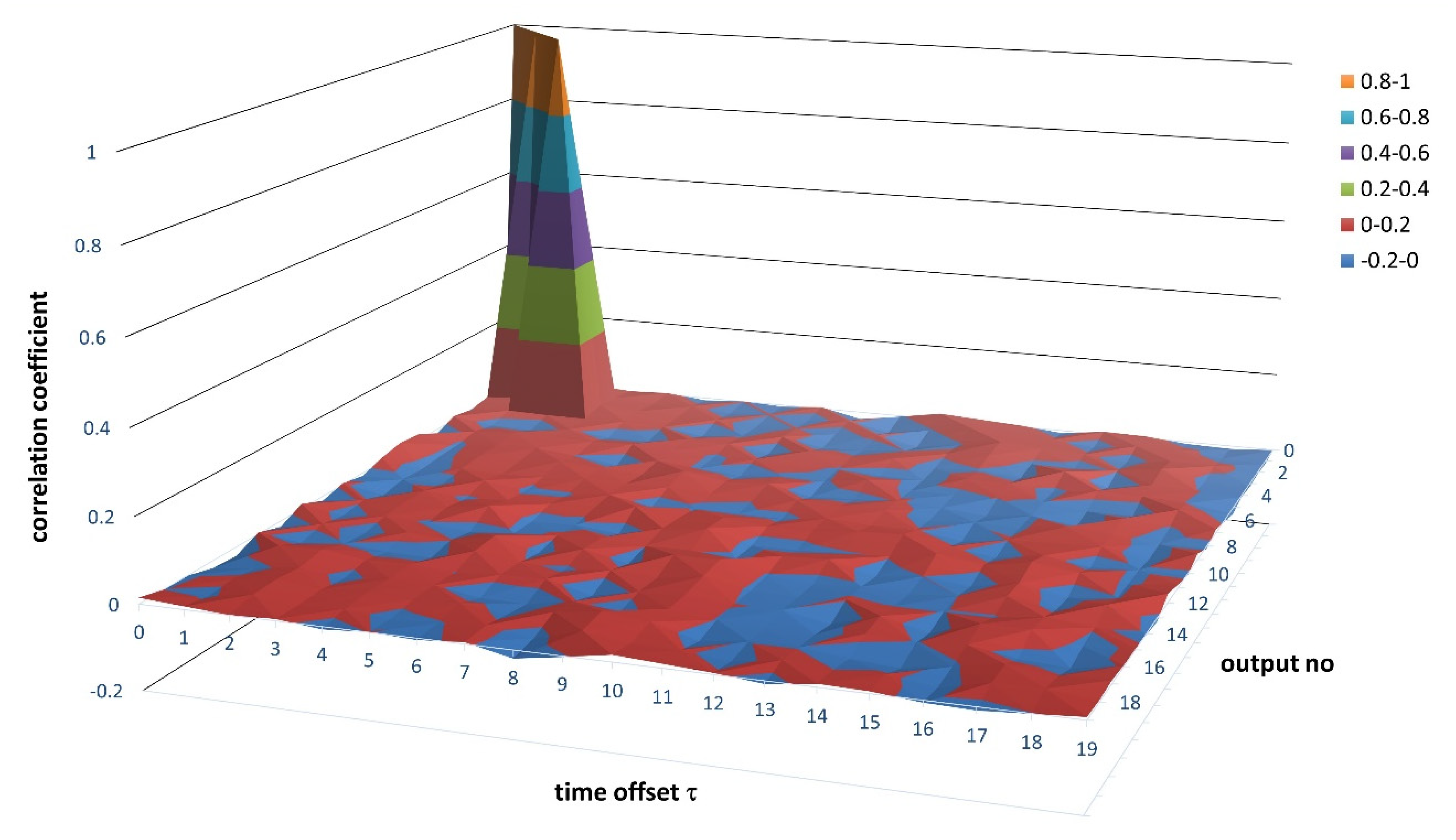
4.2. Correlations between Binary Sequences at Outputs of T-type Flip-Flops Incorporated into DT-LFSRs
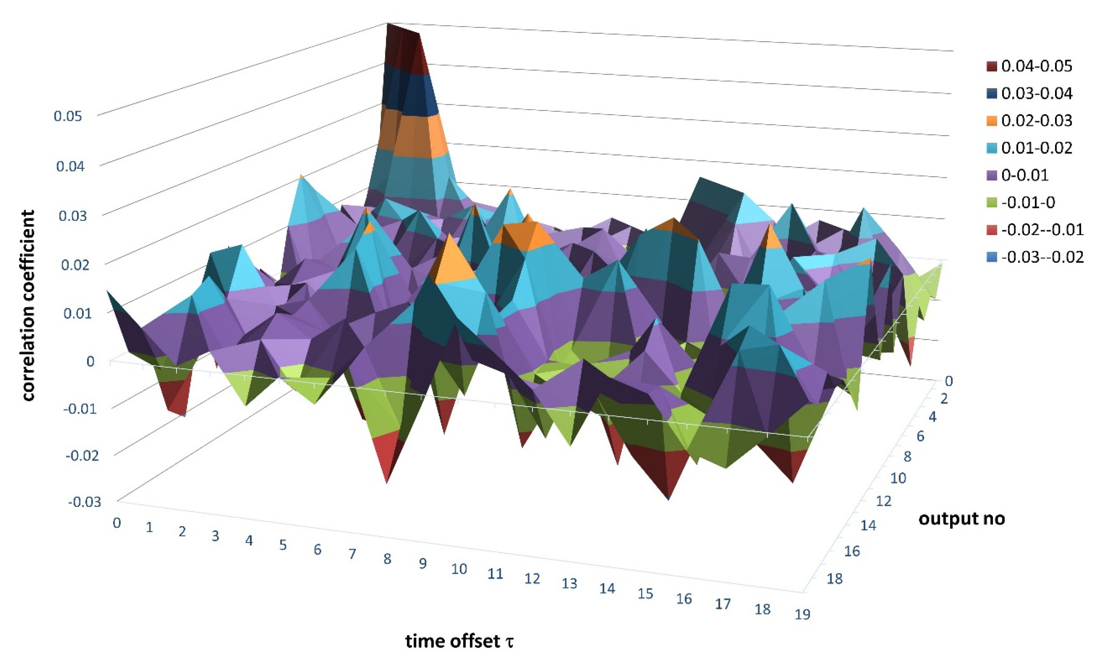
4.3. Phase Shifts between Binary Sequences at Outputs of T-type Flip-Flops Incorporated into DT-LFSRs
- Example 2
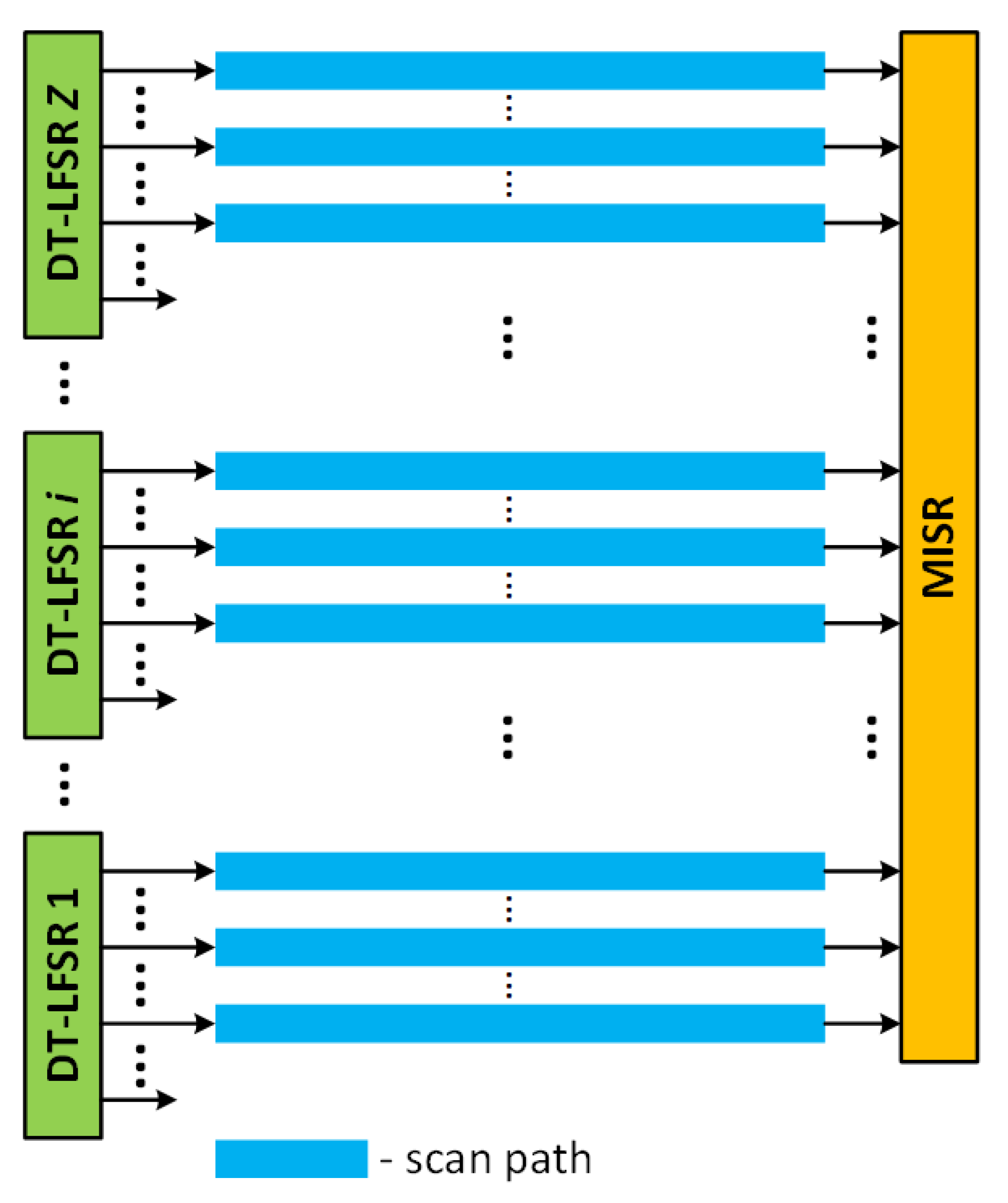
5. Pseudo-Random Pattern Generator DT-LFSR-TPG for LBIST Circuits with the STUMPS Architecture
6. Results of Logic Synthesis
7. Discussion and Conclusions
Funding
Institutional Review Board Statement
Informed Consent Statement
Data Availability Statement
Conflicts of Interest
References
- Bardell, P.H.; McAnney, W.H. Self-Testing of Multichip Logic Modules. In Proceedings of the International Test Conference, Philadelphia, PA, USA, 15–18 November 1982; pp. 200–204. [Google Scholar]
- Mourad, S.; Zorian, Y. Principles of Testing Electronic Systems, 1st ed.; John Willey & Sons: Hoboken, NJ, USA, 2000. [Google Scholar]
- Stroud, C.E. A Designer’s Guide to Built-In Self-Test, 1st ed.; Springer: Boston, MA, USA, 2002. [Google Scholar] [CrossRef]
- Bushnell, M.; Agraval, V.D. Essentials of Electronic Testing for Digital, Memory and Mixed-Signal VLSI Circuits, 1st ed.; Springer: Boston, MA, USA, 2002. [Google Scholar] [CrossRef]
- Milewski, S.; Mukherjee, N.; Rajski, J.; Solecki, J.; Tyszer, J.; Zawada, J. Full-Scan LBIST with Capture-Per-Cycle Hybrid Test Points. In Proceedings of the 2017 IEEE International Test Conference (ITC), Fort Worth, TX, USA, 31 October–2 November 2017. [Google Scholar] [CrossRef]
- Wohl, P.; Waicukauski, J.A.; Maston, G.A.; Colburn, J.E. XLBIST: X-Tolerant Logic BIST. In Proceedings of the 2018 IEEE International Test Conference (ITC), Phoenix, AZ, USA, 29 October–1 November 2018. [Google Scholar] [CrossRef]
- Moghaddam, E.; Mukherjee, N.; Rajski, J.; Solecki, J.; Tyszer, J.; Zawada, J. Logic BIST With Capture-Per-Clock Hybrid Test Points. IEEE Trans. Comput.-Aided Des. Integr. Circuits Syst. 2019, 38, 1028–1041. [Google Scholar] [CrossRef]
- Shintani, M.; Mino, T.; Inoue, M. LBIST-PUF: An LBIST Scheme Towards Efficient Challenge-Response Pairs Collection and Machine-Learning Attack Tolerance Improvement. In Proceedings of the 2020 IEEE 29th Asian Test Symposium (ATS), Penang, Malaysia, 23–26 November 2020. [Google Scholar] [CrossRef]
- Liu, Y.; Milewski, S.; Mrugalski, G.; Mukherjee, N.; Rajski, J.; Tyszer, J.; Włodarczak, B. X-Tolerant Compactor maXpress for In-System Test Applications With Observation Scan. IEEE Trans. Very Large Scale Integr. (VLSI) Syst. 2021, 29, 1553–1566. [Google Scholar] [CrossRef]
- Hortensius, P.D.; McLeod, R.D.; Pries, W.; Miller, D.M.; Card, H.C. Cellular automata-based pseudorandom number generators for built-in self-test. IEEE Trans. Comput.-Aided Des. Integr. Circuits Syst. 1989, 8, 842–859. [Google Scholar] [CrossRef]
- Bardell, P.H. Analysis of Cellular Automata Used as Pseudorandom Pattern Generators. In Proceedings of the International Test Conference, Washington, DC, USA, 10–14 September 1990. [Google Scholar] [CrossRef]
- Rajski, J.; Mrugalski, G.; Tyszer, J. Comparative study of CA-based PRPGs and LFSRs with phase shifters. In Proceedings of the 17th IEEE VLSI Test Symposium, Dana Point, CA, USA, 25–29 April 1999. [Google Scholar] [CrossRef]
- Jenkins, C.; Kakade, J.; Kagaris, D. Cellular Automata with Large Channel Separations. In Proceedings of the 2007 IEEE International Symposium on Circuits and Systems, New Orleans, LA, USA, 27–30 May 2007; pp. 1033–1036. [Google Scholar] [CrossRef]
- Chidambaram, S.; Kagaris, D.; Pradhan, D.K. Comparative study of CA with phase shifters and GLFSRs. In Proceedings of the 2005 IEEE International Conference on Test, Austin, TX, USA, 8–10 November 2005. [Google Scholar] [CrossRef]
- Kakade, J.; Kagaris, D.; Pradhan, D.K. Evaluation of Generalized LFSRs as Test Pattern Generators in Two-Dimensional Scan Designs. IEEE Trans. Comput.-Aided Des. Integr. Circuits Syst. 2008, 27, 1689–1692. [Google Scholar] [CrossRef]
- Pradhan, D.K.; Chatterjee, M. GLFSR—A New Test Pattern Generator for Built-in-Self-Test. IEEE Trans. Comput.-Aided Des. Integr. Circuits Syst. 1999, 18, 238–247. [Google Scholar] [CrossRef]
- Matsushima, J.; Maeda, Y.; Takakura, M. CooLBIST: An Effective Approach of Test Power Reduction for LBIST. In Proceedings of the 2008 17th Asian Test Symposium (ATS), Hokkaido, Japan, 24–27 November 2008. [Google Scholar] [CrossRef]
- Jayalakshmi, A.; Cheong, T.E. A Methodology for LBIST Logic Diagnosis in High Volume Manufacturing. In Proceedings of the 2012 4th Asia Symposium on Quality Electronic Design (ASQED), Penang, Malaysia, 10–11 July 2012; pp. 249–253. [Google Scholar] [CrossRef]
- Prabhu, S.; Acharya, V.V.; Bagri, S.; Hsiao, M.S. A Diagnosis-Friendly LBIST Architecture with Property Checking. In Proceedings of the 2014 IEEE International Test Conference (ITC), Seattle, WA, USA, 20–23 October 2014. [Google Scholar] [CrossRef]
- Contreras, G.K.; Zhao, Y.; Ahmed, N.; Winemberg, L.; Tehranipoor, M. LBIST Pattern Reduction by Learning ATPG Test Cube Properties. In Proceedings of the Sixteenth International Symposium on Quality Electronic Design (ISQED), Santa Clara, CA, USA, 2–4 March 2015; pp. 147–153. [Google Scholar] [CrossRef]
- Moghaddam, E.; Mukherjee, N.; Rajski, J.; Tyszer, J.; Zawada, J. Test point insertion in hybrid test compression/LBIST architectures. In Proceedings of the 2016 IEEE International Test Conference (ITC), Fort Worth, TX, USA, 15–17 November 2016. [Google Scholar] [CrossRef]
- Acevedo, O.; Kagaris, D. LFSR characteristic polynomial and phase shifter computation for two-dimensional test set generation. In Proceedings of the 2017 18th IEEE Latin American Test Symposium (LATS), Bogota, Colombia, 13–15 March 2017. [Google Scholar] [CrossRef]
- Omaña, M.; Rossi, D.; Fuzzi, F.; Metra, C.; Tirumurti, C.C.; Galivanche, R. Scalable Approach for Power Droop Reduction During Scan-Based Logic BIST. IEEE Trans. Very Large Scale Integr. (VLSI) Syst. 2017, 25, 238–246. [Google Scholar] [CrossRef] [Green Version]
- Xiang, D.; Wen, X.; Wang, L.-T. Low-Power Scan-Based Built-In Self-Test Based on Weighted Pseudorandom Test Pattern Generation and Reseeding. IEEE Trans. Very Large Scale Integr. (VLSI) Syst. 2017, 25, 942–953. [Google Scholar] [CrossRef]
- Mukherjee, N.; Tille, D.; Sapati, M.; Liu, Y.; Mayer, J.; Milewski, S.; Moghaddam, E.; Rajski, J.; Solecki, J.; Tyszer, J. Test Time and Area Optimized BIST Scheme for Automotive ICs. In Proceedings of the 2019 IEEE International Test Conference (ITC), Washington, DC, USA, 9–15 November 2019. [Google Scholar] [CrossRef]
- Kato, T.; Wang, S.; Sato, Y.; Kajihara, S.; Wen, X. A Flexible Scan-in Power Control Method in Logic BIST and Its Evaluation with TEG Chips. IEEE Trans. Emerg. Top. Comput. 2020, 8, 591–601. [Google Scholar] [CrossRef]
- Contreras, G.; Ahmed, N.; Winemberg, L.; Tehranipoor, M. Predictive LBIST Model and Partial ATPG for Seed Extraction. In Proceedings of the 2015 IEEE International Symposium on Defect and Fault Tolerance in VLSI and Nanotechnology Systems (DFTS), Amherst, MA, USA, 12–14 October 2015; pp. 139–146. [Google Scholar] [CrossRef]
- Mrugalski, G.; Rajski, J.; Rybak, Ł.; Solecki, J.; Tyszer, J. Star-EDT: Deterministic on-chip scheme using compressed test patterns. IEEE Trans. Comput.-Aided Des. Integr. Circuits Syst. 2017, 36, 683–693. [Google Scholar] [CrossRef]
- Papameletis, C.; Chickermane, V.; Foutz, B.; Singhal, S.; Chakravadhanula, K. Optimized Physical DFT Synthesis of Unified Compression and LBIST for Automotive Applications. In Proceedings of the 2019 IEEE International Test Conference (ITC), Washington, DC, USA, 9–15 November 2019. [Google Scholar] [CrossRef]
- Kumar, P.A.; Anita, J.P. Implementation of Hybrid LBIST Mechanism in Digital Circuits for Test Pattern Generation and Test Time Reduction. In Proceedings of the 2020 5th International Conference on Communication and Electronics Systems (ICCES), Coimbatore, India, 10–12 June 2020; pp. 243–248. [Google Scholar] [CrossRef]
- Liu, Y.; Mukherjee, N.; Rajski, J.; Reddy, S.M.; Tyszer, J. Deterministic Stellar BIST for automotive ICs. IEEE Trans. Comput.-Aided Des. Integr. Circuits Syst. 2020, 39, 1699–1710. [Google Scholar] [CrossRef]
- Kaczmarek, B.; Mrugalski, G.; Mukherjee, N.; Pogiel, A.; Rajski, J.; Rybak, Ł.; Tyszer, J. LBIST for Automotive ICs with Enhanced Test Generation. IEEE Trans. Comput.-Aided Des. Integr. Circuits Syst. 2021. [Google Scholar] [CrossRef]
- Golomb, S.W. Shift Register Sequences, 3rd ed.; World Scientific Publishing: Singapore, 2017; pp. 24–89. [Google Scholar] [CrossRef] [Green Version]
- Rajski, J.; Tamarapalli, N.; Tyszer, J. Automated Synthesis of Phase Shifters for Built-In Self-Test Applications. IEEE Trans. Comput.-Aided Des. Integr. Circuits Syst. 2000, 19, 1175–1188. [Google Scholar] [CrossRef]
- Rajski, J.; Tamarapalli, N.; Tyszer, J. Automated Synthesis of Large Phase Shifters for Built-In Self-Test. In Proceedings of the IEEE International Test Conference, Washington, DC, USA, 18–22 October 1998; pp. 1047–1056. [Google Scholar] [CrossRef]
- Rajski, J.; Tyszer, J. Design of Phase Shifters for BIST Applications. In Proceedings of the 16th IEEE VLSI Test Symposium, Monterey, CA, USA, 30 April 1998; pp. 218–224. [Google Scholar] [CrossRef]
- Kagaris, D. Built-In TPG with Designed Phaseshifts. In Proceedings of the 21st IEEE VLSI Test Symposium, Napa, CA, USA, 27 April–1 May 2003. [Google Scholar] [CrossRef]
- Garbolino, T.; Hławiczka, A. A New LFSR with D and T Flip-Flops as an Effective Test Pattern Generator for VLSI Circuits, In Dependable Computing—EDCC-3. EDCC 1999. Lecture Notes in Computer Science; Springer: Berlin/Heidelberg, Germany, 1999; Volume 1667, pp. 321–338. [Google Scholar] [CrossRef]
- Mrugalski, G.; Rajski, J.; Tyszer, J. Cellular Automata-Based Test Pattern Generators with Phase Shifters. IEEE Trans. Comput.-Aided Des. Integr. Circuits Syst. 2000, 19, 878–893. [Google Scholar] [CrossRef]
- Knuth, D.E. The Art of Computer Programming, Volume 2: Seminumerical Algorithms, 3rd ed.; Addison-Wesley: Boston, MA, USA, 1997. [Google Scholar]
- Zhang, S.; Byrne, V.; Muzio, J.C.; Miller, D.M. Why Cellular Automata are Better than LFSRs as Built-In Self-Test Generators for Sequential-type Faults. In Proceedings of the IEEE International Symposium on Circuits and Systems-ISCAS ‘94, London, UK, 30 May–2 June 1994; pp. 69–72. [Google Scholar] [CrossRef]
- Cho, S.-J.; Choi, U.-S.; Kim, H.-D.; Hwang, Y.-H.; Kim, J.-G.; Heo, S.-H. New Synthesis of One-Dimensional 90/150 Linear Hybrid Group Cellular Automata. IEEE Trans. Comput.-Aided Des. Integr. Circuits Syst. 2007, 26, 1720–1724. [Google Scholar] [CrossRef]
- Nandi, S.; Chaudhuri, P.P. Additive cellular automata as an on-chip test pattern generator. In Proceedings of the 1993 IEEE 2nd Asian Test Symposium (ATS), Beijing, China, 16–18 November 1993; pp. 166–171. [Google Scholar] [CrossRef]
- Serra, M.; Slater, T.; Muzio, J.C.; Miller, D.M. The analysis of one-dimensional linear cellular automata and their aliasing properties. IEEE Trans. Comput.-Aided Des. Integr. Circuits Syst. 1990, 9, 767–778. [Google Scholar] [CrossRef] [Green Version]
- Cattell, K.; Zhang, S.; Serra, M.; Muzio, J.C. 2-by-n hybrid cellular automata with regular configuration: Theory and application. IEEE Trans. Comput. 1999, 48, 285–295. [Google Scholar] [CrossRef]
- Chen, D.; Sun, X. On effectiveness of phase shifters for pseudo-random test pattern generators. In Proceedings of the IEEE Canadian Conference on Electrical and Computer Engineering, Winnipeg, MB, Canada, 12–15 May 2002; pp. 541–546. [Google Scholar] [CrossRef]
- Li, J.; Sun, X.; Soon, K. Tree-structured Linear Cellular Automata and Their Applications as PRPGs. In Proceedings of the International Test Conference, Washington, DC, USA, 3–5 November 1997; pp. 858–867. [Google Scholar] [CrossRef]
- Chowdhury, D.R.; Sengupta, I.; Chaudhuri, P.P. A class of two-dimensional cellular automata and their applications in random pattern testing. J. Electron. Test. 1994, 5, 67–82. [Google Scholar] [CrossRef]
- Sikdar, B.K.; Ganguly, N.; Chaudhuri, P.P. Design of hierarchical cellular automata for on-chip test pattern generator. IEEE Trans. Comput.-Aided Des. Integr. Circuits Syst. 2002, 21, 1530–1539. [Google Scholar] [CrossRef]
- Chaudhuri, P.P.; Chowdhury, D.R.; Nandi, S.; Chattopadhyay, S. Additive Cellular Automata: Theory and Applications, Vol. 1; Willey-IEEE Computer Society Press: Los Alamitos, CA, USA, 1997; pp. 48–52. [Google Scholar]
- Bardell, P.H. Discrete logarithms a parallel pseudorandom pattern generator analysis method. J. Electron. Test. 1992, 3, 17–31. [Google Scholar] [CrossRef]
- Odlyzko, A.M. Discrete logarithms in finite fields and their cryptographic significance. In Advances in Cryptology. EUROCRYPT 1984. Lecture Notes in Computer Science; Beth, T., Cot, N., Ingemarsson, I., Eds.; Springer: Berlin/Heidelberg, Germany, 1985; Volume 209, pp. 224–314. [Google Scholar] [CrossRef] [Green Version]
- Koblitz, N. A Course in Number Theory and Cryptography, 2nd ed.; Springer: New York, NY, USA, 1994. [Google Scholar] [CrossRef]
- Bardel, P.H. Design Considerations for Parallel Pseudorandom Pattern Generators. J. Electron. Test. 1990, 1, 73–87. [Google Scholar] [CrossRef]
- Mrugalski, G.; Tyszer, J.; Rajski, J. Linear independence as evaluation criterion for two-dimensional test pattern generators. In Proceedings of the 18th IEEE VLSI Test Symposium, Montreal, QC, Canada, 30 April-4 May 2000; pp. 377–386. [Google Scholar] [CrossRef]
- Mrugalski, G.; Tyszer, J.; Rajski, J. Synthesis of pattern generators based on cellular automata with phase shifters. In Proceedings of the IEEE International Test Conference, Atlantic City, NJ, USA, 27–30 September 1999; pp. 368–377. [Google Scholar] [CrossRef]
- Kagaris, D. A unified method for phase shifter computation. ACM Trans. Des. Autom. Electron. Syst. 2005, 10, 157–167. [Google Scholar] [CrossRef]
- Bellos, M.; Kagaris, D.; Nikolos, D. Test Set Embedding Based on Phase Shifters. In Dependable Computing EDCC-4. EDCC 2002. Lecture Notes in Computer Science; Bondavalli, A., Thevenod-Fosse, P., Eds.; Springer: Berlin/Heidelberg, Germany, 2002; Volume 2485, pp. 90–101. [Google Scholar] [CrossRef]
- Hławiczka, A. D or T Flip-Flop Based Linear Registers. Arch. Control. Sci. A Q. Pol. Acad. Sci. 1992, 1, 249–268. [Google Scholar]
- Mrugalski, G.; Rajski, J.; Tyszer, J. Ring generators—New devices for embedded test applications. IEEE Trans. Comput.-Aided Des. Integr. Circuits Syst. 2004, 23, 1306–1320. [Google Scholar] [CrossRef]
- Modular Equation Solver. Available online: https://www.dcode.fr/modular-equation-solver (accessed on 22 September 2021).
- Rajski, J.; Tyszer, J. Primitive Polynomials Over GF(2) of Degree up to 660 with Uniformly Distributed Coefficients. J. Electron. Test. 2003, 19, 645–657. [Google Scholar] [CrossRef]
- Bhavsar, D.K.; Edmondson, J.H. Testability Strategy of the Alpha AXP 21164 Microprocessor. In Proceedings of the IEEE International Test Conference, Washington, DC, USA, 2–6 October 1994; pp. 50–59. [Google Scholar] [CrossRef]
- Bhavsar, D.K.; Edmondson, J.H. Alpha 21164 Testability Strategy. IEEE Des. Test Comput. 1997, 14, 25–33. [Google Scholar] [CrossRef]
- Garbolino, T.; Hlawiczka, A.; Kristof, A. Fast and Low-Area TPGs based on T-type Flip-Flops can be Easily Integrated to the Scan Path. In Proceedings of the IEEE European Test Workshop, Cascais, Portugal, 23–26 May 2000; pp. 161–166. [Google Scholar] [CrossRef]
- Novák, O.; Plíva, Z.; Nosek, J.; Hlawiczka, A.; Garbolino, T.; Gucwa, K. Test-Per-Clock Logic BIST with Semi-Deterministic Test Patterns and Zero-Aliasing Compactor. J. Electron. Test. 2004, 20, 109–122. [Google Scholar] [CrossRef]
- Sasao, T. Switching Theory for Logic Synthesis, 1st ed.; Springer: New York, US, 1999. [Google Scholar] [CrossRef]
- Hrynkiewicz, E.; Kołodziński, S. An Ashenhurst disjoint and non-disjoint decomposition of logic functions in Reed-Muller spectral domain. In Proceedings of the 17th International Conference Mixed Design of Integrated Circuits and Systems-MIXDES 2010, Wrocław, Poland, 24–26 June 2010; pp. 200–204. [Google Scholar] [CrossRef]
- Sasao, T. Easily testable realizations for generalized Reed-Muller expressions. IEEE Trans. Comput. 1997, 46, 709–716. [Google Scholar] [CrossRef]
- Zaitseva, E.; Levashenko, V.; Lukyanchuk, I.; Rabcan, J.; Kvassay, M.; Rusnak, P. Application of Generalized Reed–Muller Expression for Development of Non-Binary Circuits. Electronics 2020, 9, 12. [Google Scholar] [CrossRef] [Green Version]
- Kalantari, Z.; Eshghi, M.; Mohammadi, M.; Jassbi, S. General Method to Design Reversible Universal n-Bit Up/Down Counters. J. Circuits Syst. Comput. 2020, 29, 2050165. [Google Scholar] [CrossRef]
- He, Z.; Xiao, L.; Gu, F.; Ruan, L.; Huo, Z.; Li, M.; Zhu, M.; Zhang, L.; Liu, R.; Wang, X. EDOA: An efficient delay optimization approach for mixed-polarity Reed-Muller logic circuits under the unit delay model. Front. Comput. Sci. 2019, 13, 1102–1115. [Google Scholar] [CrossRef]


| No. | t | n | Ω | ΦΤ | ΦΤmin |
|---|---|---|---|---|---|
| 1 | 22 | 25 | 3.36 × 10⁷ | 2.29 × 10⁷ | 1.53 × 10⁶ |
| 2 | 25 | 31 | 2.15 × 10⁹ | 1.98 × 10⁹ | 8.59 × 10⁷ |
| 3 | 27 | 29 | 5.37 × 10⁸ | 9.94 × 10⁷ | 1.99 × 10⁷ |
| 4 | 28 | 31 | 2.15 × 10⁹ | 1.30 × 10⁹ | 7.67 × 10⁷ |
| 5 | 33 | 35 | 3.44 × 10¹⁰ | 3.33 × 10¹⁰ | 1.04 × 10⁹ |
| 6 | 38 | 41 | 2.20 × 10¹² | 2.89 × 10¹¹ | 5.79 × 10¹⁰ |
| 7 | 40 | 49 | 5.63 × 10¹⁴ | 5.49 × 10¹⁴ | 1.41 × 10¹³ |
| 8 | 42 | 47 | 1.41 × 10¹⁴ | 3.69 × 10¹³ | 3.35 × 10¹² |
| 9 | 49 | 52 | 4.50 × 10¹⁵ | 2.21 × 10¹⁵ | 9.19 × 10¹³ |
| 10 | 50 | 57 | 1.44 × 10¹⁷ | 4.90 × 10¹⁶ | 2.88 × 10¹⁵ |
| 11 | 58 | 63 | 9.22 × 10¹⁸ | 1.75 × 10¹⁸ | 1.59 × 10¹⁷ |
| 12 | 59 | 60 | 1.15 × 10¹⁸ | 3.91 × 10¹⁷ | 1.95 × 10¹⁶ |
| 13 | 59 | 68 | 2.95 × 10²⁰ | 1.35 × 10²⁰ | 5.00 × 10¹⁸ |
| 14 | 62 | 63 | 9.22 × 10¹⁸ | 1.34 × 10¹⁸ | 1.49 × 10¹⁷ |
| 15 | 62 | 71 | 2.36 × 10²¹ | 3.43 × 10²⁰ | 3.81 × 10¹⁹ |
| 16 | 65 | 71 | 2.36 × 10²¹ | 1.93 × 10²¹ | 3.63 × 10¹⁹ |
| 17 | 65 | 81 | 2.42 × 1024 | 2.08 × 1024 | 3.72 × 10²² |
| 18 | 70 | 79 | 6.04 × 10²³ | 3.20 × 10²³ | 8.64 × 10²¹ |
| 19 | 71 | 84 | 1.93 × 1025 | 5.18 × 1024 | 2.72 × 10²³ |
| 20 | 74 | 87 | 1.55 × 1026 | 1.88 × 1025 | 2.09 × 1024 |
| 21 | 78 | 95 | 3.96 × 1028 | 2.54 × 1027 | 5.08 × 1026 |
| 22 | 84 | 95 | 3.96 × 1028 | 1.93 × 1028 | 4.72 × 1026 |
| 23 | 85 | 97 | 1.58 × 1029 | 2.24 × 1028 | 1.86 × 1027 |
| 24 | 91 | 97 | 1.58 × 1029 | 1.04 × 1028 | 1.74 × 1027 |
| No. | t | n | Θmin | |||||
|---|---|---|---|---|---|---|---|---|
| 128 | 256 | 512 | 1024 | 2048 | 4096 | |||
| 1 | 22 | 25 | 11,915 | 5957 | 2978 | 1489 | 744 | 372 |
| 2 | 25 | 31 | 671,088 | 335,544 | 167,772 | 83,886 | 41,943 | 20,971 |
| 3 | 27 | 29 | 155,344 | 77,672 | 38,836 | 19,418 | 9709 | 4854 |
| 4 | 28 | 31 | 599,186 | 299,593 | 149,796 | 74,898 | 37,449 | 18,724 |
| 5 | 33 | 35 | 8,134,407 | 4,067,203 | 2,033,601 | 1,016,800 | 508,400 | 254,200 |
| 6 | 38 | 41 | 4.52 × 10⁸ | 2.26 × 10⁸ | 1.13 × 10⁸ | 5.65 × 10⁷ | 2.83 × 10⁷ | 1.41 × 10⁷ |
| 7 | 40 | 49 | 1.10 × 10¹¹ | 5.50 × 10¹⁰ | 2.75 × 10¹⁰ | 1.37 × 10¹⁰ | 6.87 × 10⁹ | 3.44 × 10⁹ |
| 8 | 42 | 47 | 2.62 × 10¹⁰ | 1.31 × 10¹⁰ | 6.54 × 1009 | 3.27 × 1009 | 1.64 × 10⁹ | 8.18 × 10⁸ |
| 9 | 49 | 52 | 7.18 × 10¹¹ | 3.59 × 10¹¹ | 1.80 × 10¹¹ | 8.98 × 10¹⁰ | 4.49 × 10¹⁰ | 2.24 × 10¹⁰ |
| 10 | 50 | 57 | 2.25 × 10¹³ | 1.13 × 10¹³ | 5.63 × 10¹² | 2.81 × 10¹² | 1.41 × 10¹² | 7.04 × 10¹¹ |
| 11 | 58 | 63 | 1.24 × 10¹⁵ | 6.21 × 10¹⁴ | 3.11 × 10¹⁴ | 1.55 × 10¹⁴ | 7.76 × 10¹³ | 3.88 × 10¹³ |
| 12 | 59 | 60 | 1.53 × 10¹⁴ | 7.63 × 10¹³ | 3.82 × 10¹³ | 1.91 × 10¹³ | 9.54 × 10¹² | 4.77 × 10¹² |
| 13 | 59 | 68 | 3.91 × 10¹⁶ | 1.95 × 10¹⁶ | 9.77 × 10¹⁵ | 4.89 × 10¹⁵ | 2.44 × 10¹⁵ | 1.22 × 10¹⁵ |
| 14 | 62 | 63 | 1.16 × 10¹⁵ | 5.81 × 10¹⁴ | 2.91 × 10¹⁴ | 1.45 × 10¹⁴ | 7.26 × 10¹³ | 3.63 × 10¹³ |
| 15 | 62 | 71 | 2.98 × 10¹⁷ | 1.49 × 10¹⁷ | 7.44 × 10¹⁶ | 3.72 × 10¹⁶ | 1.86 × 10¹⁶ | 9.30 × 10¹⁵ |
| 16 | 65 | 71 | 2.84 × 10¹⁷ | 1.42 × 10¹⁷ | 7.09 × 10¹⁶ | 3.55 × 10¹⁶ | 1.77 × 10¹⁶ | 8.87 × 10¹⁵ |
| 17 | 65 | 81 | 2.91 × 10²⁰ | 1.45 × 10²⁰ | 7.27 × 10¹⁹ | 3.63 × 10¹⁹ | 1.82 × 10¹⁹ | 9.08 × 10¹⁸ |
| 18 | 70 | 79 | 6.75 × 10¹⁹ | 3.37 × 10¹⁹ | 1.69 × 10¹⁹ | 8.43 × 10¹⁸ | 4.22 × 10¹⁸ | 2.11 × 10¹⁸ |
| 19 | 71 | 84 | 2.13 × 10²¹ | 1.06 × 10²¹ | 5.32 × 10²⁰ | 2.66 × 10²⁰ | 1.33 × 10²⁰ | 6.65 × 10¹⁹ |
| 20 | 74 | 87 | 1.63 × 10²² | 8.17 × 10²¹ | 4.08 × 10²¹ | 2.04 × 10²¹ | 1.02 × 10²¹ | 5.11 × 10²⁰ |
| 21 | 78 | 95 | 3.97 × 1024 | 1.98 × 1024 | 9.92 × 10²³ | 4.96 × 10²³ | 2.48 × 10²³ | 1.24 × 10²³ |
| 22 | 84 | 95 | 3.68 × 1024 | 1.84 × 1024 | 9.21 × 10²³ | 4.61 × 10²³ | 2.30 × 10²³ | 1.15 × 10²³ |
| 23 | 85 | 97 | 1.46 × 1025 | 7.28 × 1024 | 3.64 × 1024 | 1.82 × 1024 | 9.10 × 10²³ | 4.55 × 10²³ |
| 24 | 91 | 97 | 1.36 × 1025 | 6.80 × 1024 | 3.40 × 1024 | 1.70 × 1024 | 8.50 × 10²³ | 4.25 × 10²³ |
| PRPG Type | n | Θmin | |||||
|---|---|---|---|---|---|---|---|
| 128 | 256 | 512 | 1024 | 2048 | 4096 | ||
| LFSR I [34] | 24 | 2019 | 1989 | 1938 | 1827 | 1630 | 1362 |
| 32 | 4991 | 4991 | 4990 | 4987 | 4982 | 4971 | |
| LFSR II [34] | 24 | 3437 | 3346 | 3194 | 2920 | 2454 | 1908 |
| 32 | 13,477 | 13,473 | 13,465 | 13,442 | 13,395 | 13,309 | |
| LHCA 90/150 [39] | 24 | 10,858 | 10,031 | 8713 | 6902 | 4863 | 3063 |
| 32 | 39,731 | 39,677 | 39,584 | 39,398 | 39,018 | 38,301 | |
| No. | t | n | Θmin | ||||||||
|---|---|---|---|---|---|---|---|---|---|---|---|
| 105 | 106 | 107 | 108 | 109 | 1010 | 1011 | 1012 | 1013 | |||
| 1 | 22 | 25 | 15 | 1 | - | - | - | - | - | - | - |
| 2 | 25 | 31 | 858 | 85 | 8 | - | - | - | - | - | - |
| 3 | 27 | 29 | 198 | 19 | 1 | - | - | - | - | - | - |
| 4 | 28 | 31 | 766 | 76 | 7 | - | - | - | - | - | - |
| 5 | 33 | 35 | 10,412 | 1041 | 104 | 10 | 1 | - | - | - | - |
| 6 | 38 | 41 | 578,690 | 57,869 | 5786 | 578 | 57 | 5 | - | - | - |
| 7 | 40 | 49 | 1.41 × 10⁸ | 14,073,748 | 1,407,374 | 140,737 | 14,073 | 1407 | 140 | 14 | 1 |
| 8 | 42 | 47 | 33,508,925 | 3,350,892 | 335,089 | 33,508 | 3350 | 335 | 33 | 3 | - |
| 9 | 49 | 52 | 9.19 × 10⁸ | 91,910,196 | 9,191,019 | 919,101 | 91,910 | 9191 | 919 | 91 | 9 |
| 10 | 50 | 57 | 2.88 × 10¹⁰ | 2.88 × 10⁹ | 2.88 × 10⁸ | 28,823,037 | 2,882,303 | 288,230 | 28,823 | 2882 | 288 |
| 11 | 58 | 63 | 1.59 × 10¹² | 1.59 × 10¹¹ | 1.59 × 10¹⁰ | 1.59 × 10⁹ | 1.59 × 10⁸ | 15,902,365 | 1,590,236 | 159,023 | 15,902 |
| 12 | 59 | 60 | 1.95 × 10¹¹ | 1.95 × 10¹⁰ | 1.95 × 10⁹ | 1.95 × 10⁸ | 19,541,042 | 1,954,104 | 195,410 | 19,541 | 1954 |
| 13 | 59 | 68 | 5.00 × 10¹³ | 5.00 × 10¹² | 5.00 × 10¹¹ | 5.00 × 10¹⁰ | 5.00 × 10⁹ | 5.00 × 10⁸ | 50,025,068 | 5,002,506 | 500,250 |
| 14 | 62 | 63 | 1.49 × 10¹² | 1.49 × 10¹¹ | 1.49 × 10¹⁰ | 1.49 × 10⁹ | 1.49 × 10⁸ | 14,876,406 | 1,487,640 | 148,764 | 14,876 |
| 15 | 62 | 71 | 3.81 × 10¹⁴ | 3.81 × 10¹³ | 3.81 × 10¹² | 3.81 × 10¹¹ | 3.81 × 10¹⁰ | 3.81 × 10⁹ | 3.81 × 10⁸ | 38,083,600 | 3,808,360 |
| 16 | 65 | 71 | 3.63 × 10¹⁴ | 3.63 × 10¹³ | 3.63 × 10¹² | 3.63 × 10¹¹ | 3.63 × 10¹⁰ | 3.63 × 10⁹ | 3.63 × 10⁸ | 36,325,896 | 3,632,589 |
| 17 | 65 | 81 | 3.72 × 10¹⁷ | 3.72 × 10¹⁶ | 3.72 × 10¹⁵ | 3.72 × 10¹⁴ | 3.72 × 10¹³ | 3.72 × 10¹² | 3.72 × 10¹¹ | 3.72 × 10¹⁰ | 3.72 × 10⁹ |
| 18 | 70 | 79 | 8.64 × 10¹⁶ | 8.64 × 10¹⁵ | 8.64 × 10¹⁴ | 8.64 × 10¹³ | 8.64 × 10¹² | 8.64 × 10¹¹ | 8.64 × 10¹⁰ | 8.64 × 10⁹ | 8.64 × 10⁸ |
| 19 | 71 | 84 | 2.72 × 10¹⁸ | 2.72 × 10¹⁷ | 2.72 × 10¹⁶ | 2.72 × 10¹⁵ | 2.72 × 10¹⁴ | 2.72 × 10¹³ | 2.72 × 10¹² | 2.72 × 10¹¹ | 2.72 × 10¹⁰ |
| 20 | 74 | 87 | 2.09 × 10¹⁹ | 2.09 × 10¹⁸ | 2.09 × 10¹⁷ | 2.09 × 10¹⁶ | 2.09 × 10¹⁵ | 2.09 × 10¹⁴ | 2.09 × 10¹³ | 2.09 × 10¹² | 2.09 × 10¹¹ |
| 21 | 78 | 95 | 5.08 × 10²¹ | 5.08 × 10²⁰ | 5.08 × 10¹⁹ | 5.08 × 10¹⁸ | 5.08 × 10¹⁷ | 5.08 × 10¹⁶ | 5.08 × 10¹⁵ | 5.08 × 10¹⁴ | 5.08 × 10¹³ |
| 22 | 84 | 95 | 4.72 × 10²¹ | 4.72 × 10²⁰ | 4.72 × 10¹⁹ | 4.72 × 10¹⁸ | 4.72 × 10¹⁷ | 4.72 × 10¹⁶ | 4.72 × 10¹⁵ | 4.72 × 10¹⁴ | 4.72 × 10¹³ |
| 23 | 85 | 97 | 1.86 × 10²² | 1.86 × 10²¹ | 1.86 × 10²⁰ | 1.86 × 10¹⁹ | 1.86 × 10¹⁸ | 1.86 × 10¹⁷ | 1.86 × 10¹⁶ | 1.86 × 10¹⁵ | 1.86 × 10¹⁴ |
| 24 | 91 | 97 | 1.74 × 10²² | 1.74 × 10²¹ | 1.74 × 10²⁰ | 1.74 × 10¹⁹ | 1.74 × 10¹⁸ | 1.74 × 10¹⁷ | 1.74 × 10¹⁶ | 1.74 × 10¹⁵ | 1.74 × 10¹⁴ |
| No. | t | n | Number of Scan Paths | ||||||
|---|---|---|---|---|---|---|---|---|---|
| 128 | 256 | 512 | 1024 | 2048 | 4096 | 8192 | |||
| 1 | 22 | 25 | 1.19 × 10⁴ | 5.96 × 10³ | 2.98 × 10³ | 1.49 × 10³ | 7.44 × 10² | 3.72 × 10² | 1.86 × 10² |
| 2 | 25 | 31 | 6.71 × 10⁵ | 3.36 × 10⁵ | 1.68 × 10⁵ | 8.39 × 10⁴ | 4.19 × 10⁴ | 2.10 × 10⁴ | 1.05 × 10⁴ |
| 3 | 27 | 29 | 1.55 × 10⁵ | 7.77 × 10⁴ | 3.88 × 10⁴ | 1.94 × 10⁴ | 9.71 × 10³ | 4.85 × 10³ | 2.43 × 10³ |
| 4 | 28 | 31 | 5.99 × 10⁵ | 3.00 × 10⁵ | 1.50 × 10⁵ | 7.49 × 10⁴ | 3.74 × 10⁴ | 1.87 × 10⁴ | 9.36 × 10³ |
| 5 | 33 | 35 | 8.13 × 10⁶ | 4.07 × 10⁶ | 2.03 × 10⁶ | 1.02 × 10⁶ | 5.08 × 10⁵ | 2.54 × 10⁵ | 1.27 × 10⁵ |
| 6 | 38 | 41 | 4.52 × 10⁸ | 2.26 × 10⁸ | 1.13 × 10⁸ | 5.65 × 10⁷ | 2.83 × 10⁷ | 1.41 × 10⁷ | 7.06 × 10⁶ |
| 7 | 40 | 49 | 1.10 × 10¹¹ | 5.50 × 10¹⁰ | 2.75 × 10¹⁰ | 1.37 × 10¹⁰ | 6.87 × 10⁹ | 3.44 × 10⁹ | 1.72 × 10⁹ |
| 8 | 42 | 47 | 2.62 × 10¹⁰ | 1.31 × 10¹⁰ | 6.54 × 10⁹ | 3.27 × 10⁹ | 1.64 × 10⁹ | 8.18 × 10⁸ | 4.09 × 10⁸ |
| 9 | 49 | 52 | 7.18 × 10¹¹ | 3.59 × 10¹¹ | 1.80 × 10¹¹ | 8.98 × 10¹⁰ | 4.49 × 10¹⁰ | 2.24 × 10¹⁰ | 1.12 × 10¹⁰ |
| 10 | 50 | 57 | 2.25 × 10¹³ | 1.13 × 10¹³ | 5.63 × 10¹² | 2.81 × 10¹² | 1.41 × 10¹² | 7.04 × 10¹¹ | 3.52 × 10¹¹ |
| 11 | 58 | 63 | 1.24 × 10¹⁵ | 6.21 × 10¹⁴ | 3.11 × 10¹⁴ | 1.55 × 10¹⁴ | 7.76 × 10¹³ | 3.88 × 10¹³ | 1.94 × 10¹³ |
| 12 | 59 | 60 | 1.53 × 10¹⁴ | 7.63 × 10¹³ | 3.82 × 10¹³ | 1.91 × 10¹³ | 9.54 × 10¹² | 4.77 × 10¹² | 2.39 × 10¹² |
| 13 | 59 | 68 | 3.91 × 10¹⁶ | 1.95 × 10¹⁶ | 9.77 × 10¹⁵ | 4.89 × 10¹⁵ | 2.44 × 10¹⁵ | 1.22 × 10¹⁵ | 6.11 × 10¹⁴ |
| 14 | 62 | 63 | 1.16 × 10¹⁵ | 5.81 × 10¹⁴ | 2.91 × 10¹⁴ | 1.45 × 10¹⁴ | 7.26 × 10¹³ | 3.63 × 10¹³ | 1.82 × 10¹³ |
| 15 | 62 | 71 | 2.98 × 10¹⁷ | 1.49 × 10¹⁷ | 7.44 × 10¹⁶ | 3.72 × 10¹⁶ | 1.86 × 10¹⁶ | 9.30 × 10¹⁵ | 4.65 × 10¹⁵ |
| 16 | 65 | 71 | 2.84 × 10¹⁷ | 1.42 × 10¹⁷ | 7.09 × 10¹⁶ | 3.55 × 10¹⁶ | 1.77 × 10¹⁶ | 8.87 × 10¹⁵ | 4.43 × 10¹⁵ |
| 17 | 65 | 81 | 2.91 × 10²⁰ | 1.45 × 10²⁰ | 7.27 × 10¹⁹ | 3.63 × 10¹⁹ | 1.82 × 10¹⁹ | 9.08 × 10¹⁸ | 4.54 × 10¹⁸ |
| 18 | 70 | 79 | 6.75 × 10¹⁹ | 3.37 × 10¹⁹ | 1.69 × 10¹⁹ | 8.43 × 10¹⁸ | 4.22 × 10¹⁸ | 2.11 × 10¹⁸ | 1.05 × 10¹⁸ |
| 19 | 71 | 84 | 2.13 × 10²¹ | 1.06 × 10²¹ | 5.32 × 10²⁰ | 2.66 × 10²⁰ | 1.33 × 10²⁰ | 6.65 × 10¹⁹ | 3.33 × 10¹⁹ |
| 20 | 74 | 87 | 1.63 × 10²² | 8.17 × 10²¹ | 4.08 × 10²¹ | 2.04 × 10²¹ | 1.02 × 10²¹ | 5.11 × 10²⁰ | 2.55 × 10²⁰ |
| 21 | 78 | 95 | 3.97 × 1024 | 1.98 × 1024 | 9.92 × 10²³ | 4.96 × 10²³ | 2.48 × 10²³ | 1.24 × 10²³ | 6.20 × 10²² |
| 22 | 84 | 95 | 3.68 × 1024 | 1.84 × 1024 | 9.21 × 10²³ | 4.61 × 10²³ | 2.30 × 10²³ | 1.15 × 10²³ | 5.76 × 10²² |
| 23 | 85 | 97 | 1.46 × 1025 | 7.28 × 1024 | 3.64 × 1024 | 1.82 × 1024 | 9.10 × 10²³ | 4.55 × 10²³ | 2.28 × 10²³ |
| 24 | 91 | 97 | 1.36 × 1025 | 6.80 × 1024 | 3.40 × 1024 | 1.70 × 1024 | 8.50 × 10²³ | 4.25 × 10²³ | 2.13 × 10²³ |
| No. | t | n | Total Cost | Cost Per Channel |
|---|---|---|---|---|
| 1 | 22 | 25 | 176 | 8.00 |
| 2 | 25 | 31 | 212 | 8.48 |
| 3 | 27 | 29 | 209 | 7.74 |
| 4 | 28 | 31 | 220 | 7.86 |
| 5 | 33 | 35 | 253 | 7.67 |
| 6 | 38 | 41 | 294 | 7.74 |
| 7 | 40 | 49 | 335 | 8.38 |
| 8 | 42 | 47 | 332 | 7.90 |
| 9 | 49 | 52 | 374 | 7.63 |
| 10 | 50 | 57 | 400 | 8.00 |
| 11 | 58 | 63 | 449 | 7.74 |
| 12 | 59 | 60 | 439 | 7.44 |
| 13 | 59 | 68 | 474 | 8.03 |
| 14 | 62 | 63 | 461 | 7.44 |
| 15 | 62 | 71 | 496 | 8.00 |
| 16 | 65 | 71 | 505 | 7.77 |
| 17 | 65 | 81 | 549 | 8.45 |
| 18 | 70 | 79 | 555 | 7.93 |
| 19 | 71 | 84 | 580 | 8.17 |
| 20 | 74 | 87 | 602 | 8.14 |
| 21 | 78 | 95 | 649 | 8.32 |
| 22 | 84 | 95 | 667 | 7.94 |
| 23 | 85 | 97 | 678 | 7.98 |
| 24 | 91 | 97 | 696 | 7.65 |
| No. | t | n | Number of Scan Paths | |||||
|---|---|---|---|---|---|---|---|---|
| 128 | 256 | 512 | 1024 | 2048 | 4096 | |||
| 1 | 22 | 25 | 1056 | 2112 | 4224 | 8272 | 16,544 | 32,912 |
| 2 | 25 | 31 | 1272 | 2332 | 4452 | 8692 | 17,384 | 34,768 |
| 3 | 27 | 29 | 1045 | 2090 | 3971 | 7942 | 15,884 | 31,768 |
| 4 | 28 | 31 | 1100 | 2200 | 4180 | 8140 | 16,280 | 32,340 |
| 5 | 33 | 35 | 1012 | 2024 | 4048 | 8096 | 15,939 | 31,625 |
| 6 | 38 | 41 | 1176 | 2058 | 4116 | 7938 | 15,876 | 31,752 |
| 7 | 40 | 49 | 1340 | 2345 | 4355 | 8710 | 17,420 | 34,505 |
| 8 | 42 | 47 | 1328 | 2324 | 4316 | 8300 | 16,268 | 32,536 |
| 9 | 49 | 52 | 1122 | 2244 | 4114 | 7854 | 15,708 | 31,416 |
| 10 | 50 | 57 | 1200 | 2400 | 4400 | 8400 | 16,400 | 32,800 |
| 11 | 58 | 63 | 1347 | 2245 | 4041 | 8082 | 16,164 | 31,879 |
| 12 | 59 | 60 | 1317 | 2195 | 3951 | 7902 | 15,365 | 30,730 |
| 13 | 59 | 68 | 1422 | 2370 | 4266 | 8532 | 16,590 | 33,180 |
| 14 | 62 | 63 | 1383 | 2305 | 4149 | 7837 | 15,674 | 30,887 |
| 15 | 62 | 71 | 1488 | 2480 | 4464 | 8432 | 16,864 | 33,232 |
| 16 | 65 | 71 | 1010 | 2020 | 4040 | 8080 | 16,160 | 32,320 |
| 17 | 65 | 81 | 1098 | 2196 | 4392 | 8784 | 17,568 | 35,136 |
| 18 | 70 | 79 | 1110 | 2220 | 4440 | 8325 | 16,650 | 32,745 |
| 19 | 71 | 84 | 1160 | 2320 | 4640 | 8700 | 16,820 | 33,640 |
| 20 | 74 | 87 | 1204 | 2408 | 4214 | 8428 | 16,856 | 33,712 |
| 21 | 78 | 95 | 1298 | 2596 | 4543 | 9086 | 17,523 | 34,397 |
| 22 | 84 | 95 | 1334 | 2668 | 4669 | 8671 | 16,675 | 32,683 |
| 23 | 85 | 97 | 1356 | 2712 | 4746 | 8814 | 16,950 | 33,222 |
| 24 | 91 | 97 | 1392 | 2088 | 4176 | 8352 | 16,008 | 32,016 |
| No. | t | n | Number of Scan Paths | |||||
|---|---|---|---|---|---|---|---|---|
| 128 | 256 | 512 | 1024 | 2048 | 4096 | |||
| 1 | 22 | 25 | 6, 18, 4 | 12, 36, 8 | 24, 72, 16 | 47, 141, 10 | 94, 282, 20 | 187, 561, 18 |
| 2 | 25 | 31 | 6, 36, 22 | 11, 66, 19 | 21, 126, 13 | 41, 246, 1 | 82, 492, 2 | 164, 984, 4 |
| 3 | 27 | 29 | 5, 10, 7 | 10, 20, 14 | 19, 38, 1 | 38, 76, 2 | 76, 152, 4 | 152, 304, 8 |
| 4 | 28 | 31 | 5, 15, 12 | 10, 30, 24 | 19, 57, 20 | 37, 111, 12 | 74, 222, 24 | 147, 441, 20 |
| 5 | 33 | 35 | 4, 8, 4 | 8, 16, 8 | 16, 32, 16 | 32, 64, 32 | 63, 126, 31 | 125, 250, 29 |
| 6 | 38 | 41 | 4, 12, 24 | 7, 21, 10 | 14, 42, 20 | 27, 81, 2 | 54, 162, 4 | 108, 324, 8 |
| 7 | 40 | 49 | 4, 36, 32 | 7, 63, 24 | 13, 117, 8 | 26, 234, 16 | 52, 468, 32 | 103, 927, 24 |
| 8 | 42 | 47 | 4, 20, 40 | 7, 35, 38 | 13, 65, 34 | 25, 125, 26 | 49, 245, 10 | 98, 490, 20 |
| 9 | 49 | 52 | 3, 9, 19 | 6, 18, 38 | 11, 33, 27 | 21, 63, 5 | 42, 126, 10 | 84, 252, 20 |
| 10 | 50 | 57 | 3, 21, 22 | 6, 42, 44 | 11, 77, 38 | 21, 147, 26 | 41, 287, 2 | 82, 574, 4 |
| 11 | 58 | 63 | 3, 15, 46 | 5, 25, 34 | 9, 45, 10 | 18, 90, 20 | 36, 180, 40 | 71, 355, 22 |
| 12 | 59 | 60 | 3, 3, 49 | 5, 5, 39 | 9, 9, 19 | 18, 18, 38 | 35, 35, 17 | 70, 70, 34 |
| 13 | 59 | 68 | 3, 27, 49 | 5, 45, 39 | 9, 81, 19 | 18, 162, 38 | 35, 315, 17 | 70, 630, 34 |
| 14 | 62 | 63 | 3, 3, 58 | 5, 5, 54 | 9, 9, 46 | 17, 17, 30 | 34, 34, 60 | 67, 67, 58 |
| 15 | 62 | 71 | 3, 27, 58 | 5, 45, 54 | 9, 81, 46 | 17, 153, 30 | 34, 306, 60 | 67, 603, 58 |
| 16 | 65 | 71 | 2, 12, 2 | 4, 24, 4 | 8, 48, 8 | 16, 96, 16 | 32, 192, 32 | 64, 384, 64 |
| 17 | 65 | 81 | 2, 32, 2 | 4, 64, 4 | 8, 128, 8 | 16, 256, 16 | 32, 512, 32 | 64, 1024, 64 |
| 18 | 70 | 79 | 2, 18, 12 | 4, 36, 24 | 8, 72, 48 | 15, 135, 26 | 30, 270, 52 | 59, 531, 34 |
| 19 | 71 | 84 | 2, 26, 14 | 4, 52, 28 | 8, 104, 56 | 15, 195, 41 | 29, 377, 11 | 58, 754, 22 |
| 20 | 74 | 87 | 2, 26, 20 | 4, 52, 40 | 7, 91, 6 | 14, 182, 12 | 28, 364, 24 | 56, 728, 48 |
| 21 | 78 | 95 | 2, 34, 28 | 4, 68, 56 | 7, 119, 34 | 14, 238, 68 | 27, 459, 58 | 53, 901, 38 |
| 22 | 84 | 95 | 2, 22, 40 | 4, 44, 80 | 7, 77, 76 | 13, 143, 68 | 25, 275, 52 | 49, 539, 20 |
| 23 | 85 | 97 | 2, 24, 42 | 4, 48, 84 | 7, 84, 83 | 13, 156, 81 | 25, 300, 77 | 49, 588, 69 |
| 24 | 91 | 97 | 2, 12, 54 | 3, 18, 17 | 6, 36, 34 | 12, 72, 68 | 23, 138, 45 | 46, 276, 90 |
| Number of Scan Paths | Type I LFSRs | Type II LFSRs | ||||||||||
|---|---|---|---|---|---|---|---|---|---|---|---|---|
| h1(x) | h2(x) | h3(x) | h4(x) | h5(x) | h6(x) | h1(x) | h2(x) | h3(x) | h4(x) | h5(x) | h6(x) | |
| 128 | 459 | 527 | 603 | 667 | 725 | 862 | 461 | 525 | 588 | 656 | 717 | 864 |
| 575 | 614 | 614 * | 614 * | 614 * | 614 * | 567 | 668 | 711 | 831 | 665 | 796 | |
| 256 | 794 | 839 | 940 | 964 | 1061 | 1148 | 785 | 837 | 919 | 975 | 1054 | 1150 |
| 563 | 516 | 614 * | 582 | 588 | 515 | 584 | 536 | 659 | 642 | 641 | 697 | |
| 512 | 1306 | 1456 | 1523 | 1568 | 1650 | 1823 | 1308 | 1454 | 1508 | 1570 | 1648 | 1804 |
| 435 | 521 | 511 | 473 | 499 | 565 | 448 | 551 | 543 | 486 | 514 | 586 | |
| 1024 | 2542 | 2553 | 2650 | 2759 | 2824 | 2969 | 2430 | 2550 | 2649 | 2753 | 2822 | 2958 |
| 424 | 425 | 425 | 510 | 474 | 492 | 437 | 431 | 433 | 523 | 485 | 501 | |
| 2048 | 5008 | 4950 | 4982 | 5028 | 5131 | 5218 | 4995 | 4946 | 4980 | 5027 | 5131 | 5214 |
| 356 | 419 | 416 | 408 | 439 | 368 | 373 | 431 | 434 | 410 | 450 | 392 | |
| 4096 | 9738 | 10046 | 9622 | 9697 | 9775 | 9905 | 9641 | 10026 | 9618 | 9663 | 9757 | 9877 |
| 342 | 352 | 375 | 417 | 415 | 418 | 342 | 368 | 398 | 440 | 421 | 436 | |
| Number of Scan Paths | Type I LFSRs | Type II LFSRs | ||||||||||
|---|---|---|---|---|---|---|---|---|---|---|---|---|
| h1(x) | h2(x) | h3(x) | h4(x) | h5(x) | h6(x) | h1(x) | h2(x) | h3(x) | h4(x) | h5(x) | h6(x) | |
| 128 | 120% | 91% | 68% | 51% | 39% | 17% | 119% | 92% | 72% | 54% | 41% | 17% |
| 73% | 62% | 62% | 62% | 62% | 62% | 75% | 49% | 40% | 20% | 50% | 25% | |
| 256 | 154% | 141% | 115% | 110% | 90% | 76% | 157% | 141% | 120% | 107% | 92% | 76% |
| 76% | 93% | 62% | 71% | 69% | 93% | 70% | 86% | 51% | 55% | 55% | 43% | |
| 512 | 203% | 171% | 159% | 152% | 139% | 117% | 202% | 172% | 162% | 152% | 140% | 119% |
| 129% | 91% | 95% | 110% | 99% | 76% | 122% | 80% | 83% | 104% | 93% | 70% | |
| 1024 | 208% | 207% | 196% | 184% | 178% | 164% | 223% | 207% | 196% | 185% | 178% | 165% |
| 134% | 134% | 134% | 95% | 110% | 102% | 128% | 130% | 129% | 90% | 105% | 98% | |
| 2048 | 207% | 210% | 208% | 206% | 199% | 194% | 208% | 211% | 209% | 206% | 199% | 195% |
| 180% | 137% | 139% | 144% | 126% | 170% | 167% | 131% | 129% | 142% | 121% | 154% | |
| 4096 | 216% | 206% | 219% | 217% | 214% | 210% | 219% | 207% | 220% | 218% | 215% | 211% |
| 191% | 183% | 165% | 139% | 140% | 138% | 190% | 170% | 150% | 126% | 136% | 128% | |
Publisher’s Note: MDPI stays neutral with regard to jurisdictional claims in published maps and institutional affiliations. |
© 2021 by the author. Licensee MDPI, Basel, Switzerland. This article is an open access article distributed under the terms and conditions of the Creative Commons Attribution (CC BY) license (https://creativecommons.org/licenses/by/4.0/).
Share and Cite
Garbolino, T. A New, Fast Pseudo-Random Pattern Generator for Advanced Logic Built-In Self-Test Structures. Appl. Sci. 2021, 11, 9476. https://doi.org/10.3390/app11209476
Garbolino T. A New, Fast Pseudo-Random Pattern Generator for Advanced Logic Built-In Self-Test Structures. Applied Sciences. 2021; 11(20):9476. https://doi.org/10.3390/app11209476
Chicago/Turabian StyleGarbolino, Tomasz. 2021. "A New, Fast Pseudo-Random Pattern Generator for Advanced Logic Built-In Self-Test Structures" Applied Sciences 11, no. 20: 9476. https://doi.org/10.3390/app11209476
APA StyleGarbolino, T. (2021). A New, Fast Pseudo-Random Pattern Generator for Advanced Logic Built-In Self-Test Structures. Applied Sciences, 11(20), 9476. https://doi.org/10.3390/app11209476