Review

Light Propagation in Confined Nematic Liquid Crystals and Device Applications

by
Antonio d’Alessandro
* and
Rita Asquini
Centre of Nanotechnologies Applied to Engineering–CNIS, Department of Information Engineering, Electronics and Telecommunications, Sapienza University of Rome, 00185 Roma, Italy
*
Author to whom correspondence should be addressed.
Appl. Sci. 2021, 11(18), 8713; https://doi.org/10.3390/app11188713
Submission received: 23 August 2021 / Revised: 13 September 2021 / Accepted: 15 September 2021 / Published: 18 September 2021
(This article belongs to the Special Issue Light Beams in Liquid Crystals)

Abstract

:

Featured Applications

optical communications, optical sensors.

Abstract

Liquid crystals are interesting linear and nonlinear optical materials used to make a wide variety of devices beyond flat panel displays. Liquid crystalline materials can be used either as core or as cladding of switchable/reconfigurable waveguides with either an electrical or an optical control or both. In this paper, materials and main device structures of liquid crystals confined in different waveguide geometries are presented using different substrate materials, such as silicon, soda lime or borosilicate glass and polydimethylsiloxane. Modelling of the behaviour of liquid crystal nanometric molecular reorientation and related refractive index distribution under both low-frequency electric and intense optical fields is reported considering optical anisotropy of liquid crystals. A few examples of integrated optic devices based on waveguides using liquid crystalline materials as core for optical switching and filtering are reviewed. Reported results indicate that low-power control signals represent a significant feature of photonic devices based on light propagation in liquid crystals, with performance, which are competitive with analogous integrated optic devices based on other materials for optical communications and optical sensing systems.

1. Introduction

It is well known that the most important application of liquid crystals (LCs) nowadays is flat panel displays (FPD), which is a very mature industry. Recently, other FPD technologies, such as OLED and micro-LED, are competing with LC-FPD in many applications. However, LCs are excellent materials for light phase modulation which cannot be achieved by OLED and micro-LED. Indeed, many photonic devices/systems and applications based on LC modulations are developing.
Liquid crystalline materials used for most applications are usually made of mixtures of different compounds to optimize their electro-optical performance. LC molecules, made of ring systems, linking groups, substituents and terminal groups as sketched in Figure 1, are designed in order to optimize LC physical and optical properties.
LCs have low optical losses from UV to IR with scattering decreasing as λ−2.34 [1] gaining interest for guide wave devices [2,3]. LC have been demonstrated as effective materials to make both electrically [4] and optically [5] controlled cores for switchable and reconfigurable waveguides to be used at the wavelength of 1.55 µm in optical communications for their attractive optical properties. The efficient electro-optical effect with the additional advantage of negligible electrical current absorption and the nonlinear optical properties allow very low power consumption without appreciable energy dissipation. Linear optical properties stimulated the study and development of LC-based waveguides [6,7,8,9,10,11,12,13,14,15].
Nonlinear optical properties fostered intense research activity on the development of solitonic propagation in LC with many potential applications [16,17,18,19,20,21,22]. Photonic bandgap structures obtained by infiltrating LC in hollow optical fibres, the so-called photonic LC fibres, were also intensely studied, generating another broad research line [23,24,25,26,27]. The light characteristics make LC-based photonic devices interesting potential candidates for both datacom and optofluidic applications [28,29,30,31,32]. LC propagation properties were also interestingly investigated to generate optical vortices [33,34], which may result in an important breakthrough in the development of optical tweezers, high-order quantum entanglement and novel nonlinear optic effects with competing nonlinearities [35,36]. Another interesting effect of light propagation in LC is related to all-optical angular control of the molecular alignment in LC films due to light and matter angular momentum conservation [37,38].
More recently, LC-based optical sources were demonstrated to envision full integration of optical functionalities in a single chip using liquid crystalline materials. OLEDs were reported by employing liquid-crystalline host matrix in the emission layer [39]. Lasers were demonstrated by means of a novel approach to generate actively Q-switched laser pulses based on an integrated waveguide chip and an LC cell in the deformed helix ferroelectric (DHF) mode, able to behave like an active Q-switch modulator under a wide range of repetition frequencies [40]. Vertical cavity surface-emitting laser, including LC as a tuning medium, was also reported [41].
Despite the many interesting optical properties of LCs, it is no small undertaking to make waveguiding devices in which input and output signals can be coupled in and out by using standard optical fibres. In this paper, a review of proposed devices is presented to make optical switches and filters based on propagation properties of nematic LCs in which a signal is transmitted between two standard single mode fibres. Such devices can be integrated in many systems for several applications such as communications and sensor microsystems. In Section 2, materials and main device structures of LCs confined in different waveguide geometries are presented by focusing on fabrication issues. Section 3 reports on modelling for designing guide wave LC devices and simulations of their operation. Section 4 shows some examples of optical switches and tunable filters in which light beams are confined in oriented nematic LC channels. Section 5 reports some perspective conclusions on further research development of LC-based guided wave devices.

2. Materials and LC Waveguide Structures

LC materials can be used either to make a core of optical waveguides, in which light beams can be confined, or to make a cladding [42]. In both cases tunable or reconfigurable optical channels can be obtained by exploiting the LC electro-optic effect. LCs can be infiltrated by capillarity in different confined geometries of optical waveguides [8,9,10] or optical fibres [43].

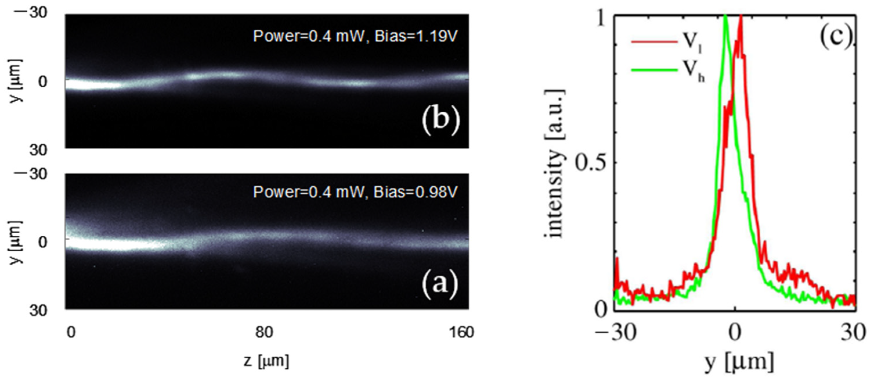
2.1. Nematic LC Confined in SiO2/Si V-grooves

A channel waveguide can be obtained by infiltrating a nematic LC in a SiO2/Si groove as shown in Figure 2a. The ITO layer and the n-Si substrate act as electrodes to apply an external electric field. A silicon V-groove is made by exploiting anisotropic etching of silicon. Typical groove width ranges from 5 to 15 µm. A native thermal oxide SiO2, obtained in an oven at about 1100 °C acts as a low index cladding, considering that a nematic LC has a refractive index higher than 1.45. The V-groove is fabricated by means of a micromachining process whose details are described in ref [44].
Figure 2b shows a scanning electron microscope picture of the V-groove in which smoothness of SiO2/Si surfaces is able to minimize defects in the embedded LC molecules, consequently attenuating light scattering in the final LC waveguide.
The etching of Si creates a V-groove with an angle α = 54.7° using (100) Si wafer as schematically shown in Figure 3a. A glass cover of 0.5 mm is then placed on top of the V-groove [4]. A D263 borosilicate glass substrate is used with a refractive index nD263 = 1.516 (at the at wavelength λ = 1.55 µm) intermediate between the values of the extraordinary and the ordinary refractive index of the LC used, such as E7 (ne = 1.69, no = 1.5 at wavelength λ = 1.55 µm), which allows the creation of an optical switch [4]. A thin film of Nylon 6 is spanned and rubbed on top of the ITO film, to align the LC along the groove. Nematic LC E7 in the isotropic phase is infiltrated in the covered V-groove by capillarity in vacuum at 80 °C and then cooled down to the room temperature. Figure 3b shows the orientation of nematic LC molecules, whose tilt angle θ is controlled by the applied voltage between the ITO and n-Si.
Light is coupled to LC waveguides in Si/SiO2 grooves, referred to as LCW (Liquid Crystal Waveguide), by fibre butt-coupling, as shown in Figure 4. Since LC-NOA61 interface was used, total coupling losses, including input and output, of 4.5 dB or better were measured, as a result of minimization of LC molecular random orientation representing a source of light scattering at the input and output faces of the LCW, which determined higher coupling losses in previous samples without LC-NOA61 interface [45]. Propagation losses resulted to be about 6 dB/cm which can be further lowered by using photoalignment techniques, able to improve the optical quality of the LCW [46,47].

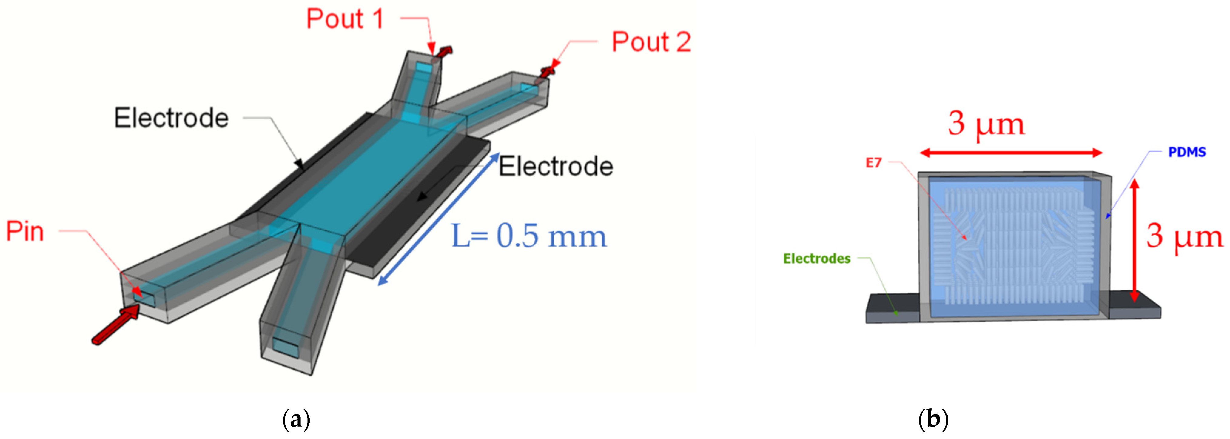
2.2. Nematic LC in PDMS Waveguides

Optical waveguides can be made by infiltrating a nematic LC in polydimethylsiloxane (PDMS) channels by capillarity. Such waveguides are referred as LC:PDMS waveguides. Use of PDMS is motivated since it is a material often used for microfluidic applications with high optical quality [48]. PDMS is optical transparent, with low surface energy in the range of 20–23 mJ/m2 at 20 °C [49], low dielectric constant in the range of 2.32–2.40 [50] and Young’s modulus, which is between 0.57 MPa and 3.7 MPa [51], and thermally and optically enabled polymerization. PDMS is also reliable for soft lithographic fabrication of many microfluidic and micro-optical devices [52].
Flexibility is another attractive feature of PDMS which is effectively used in robotics, automation, consumer electronics and in novel applications, such as health care and biomedical technologies. PDMS is used in optical interconnections for datacom applications to replace metallic connections whose performance in terms of bit rate are very low and suffer problems related to high heat dissipation [53].
PDMS channels to be filled with a nematic LC are fabricated by the cast and moulding technique involving several technological phases as shown in Figure 5 and described in ref. [31].
The PDMS channels are filled with a nematic LC by capillarity which results in homeotropically alignment as shown in Figure 6a. Homeotropic alignment of LC is due to the hydrophobic characteristic of the PDMS inner surface. A fabricate sample including LC:PDMS waveguides with widths of 8, 10 and 15 µm is reported in Figure 6b. The optical characterization to check the LC alignment in the LC:PDMS waveguides is performed using a polarized microscope. Polarized light is transmitted through the channels, revealing the homeotropic arrangement of the LC molecules. Such orientation of the LC is proven by the black part in the central region for the waveguides indicating that polarization of input light is not changed when transmitted through the LC and is stopped by the crossed analyser, as it can be observed in Figure 6c. Light leaks through the edges of the waveguides because of the optical retardation induced by the LC molecules homeotropically aligned on the vertical sides of the PDMS channels.
LC molecular orientation inside the PDMS channel induces a refractive index distribution which determines polarization-independent light propagation [31]. Green laser light at a wavelength of 532 nm and red light using an He-Ne laser source at a wavelength of 632.8 nm were efficiently fibre butt-coupled to the LC:PDMS waveguide as shown in Figure 7a. Propagation in the C-band was also studied using a tunable laser source between 1510 nm and 1590 nm. Light transmission versus polarization orientation was measured using a set-up including a polarization controller, consisting of a half-wave plate between two quarter-wave plates, an optical power meter and a polarizer at the output of the waveguide. It has been observed that light polarization does not vary as it propagates along the LC:PMDS channel for any polarization at the input. A polarization differential loss of only 0.3 dB, as shown in Figure 7b, was measured with propagation losses of about 8 dB/cm.
It is possible to control LC:PDMS waveguides by means of coplanar electrodes. Preliminary measurements show that LC molecules can be switched by applying a square voltage of 1 kHz with an amplitude of about 2 V. In this case, only change of modal propagation was affected without a substantial light transmission of light, since the core refractive index remains above the PDMS refractive index. By choosing a PDMS with a refractive index intermediate between the ordinary and the extraordinary refractive of the LC, light modulation or switching is possible.

3. Modelling of Light Propagation in Nematic LC Waveguides

Light propagation in LC waveguides is affected by the LC molecular orientation represented by a unity vector referred to as director n, as shown in Figure 8. Typical dimensions are a few nanometres along the molecular axis and about 1 nm in the perpendicular direction. Locally, a refractive index n along the molecular axis and a refractive index n perpendicular to the molecular axis are defined. In the bulk LC, an extraordinary refractive index ne and an ordinary refractive index no are defined along and perpendicularly to the director n, respectively, showing a birefringence ranging between 0.15 and 0.5, depending on the chemical compounds and wavelengths.
The optical anisotropy and the molecular orientation of the LC molecules induce the refractive index spatial distribution nLC (x,y) in the LCW determined by the electric field Eac related to the ac voltage applied to the electrodes and the optical electric field Eopt of the propagating light beam when its intensity is relatively high. The electric field dependence enables both an electro-optic and an all-optical control. The LC molecular orientation is the result of the balance between the electric torques and the elastic restoring torque when an electric field is applied. The deformation pattern affected by the elastic torque is the result of a combination of three basic deformations, which are splay, twist and bend.
The orientation of the LC is imposed by the minimum of the free energy F given by:
F = F e l F d i e l F o p t
in which Fel is the elastic term, Fdiel is the dielectric term and Fopt is the optical term related to the electric field of the optical beam propagating in the LC.
The Oseen–Frank theory indicates that the elastic energy is given by [54]:
F e l = 1 2 [ k 11 ( n ) 2 + k 22 ( n × n ) 2 + k 33 ( n × × n ) 2 ] d v
where k11, k22 and k33 are the elastic constants corresponding to the splay, twist and bend, respectively, in which v is the volume. The dielectric energy is given by:
F d i e l = 1 2 [ ε 0 ε , a c | E a c | 2 + ε 0 Δ ε a c ( E a c n ) 2 ] d v
where ε 0 is the dielectric permittivity in vacuum, ε , a c is the dielectric permittivity perpendicular to the optical axis, Δ ε a c is the dielectric anisotropy, and Eac is the applied electric field at low frequency. The optical term of the energy is given by:
F o p t = 1 2 [ ε 0 ε , o p t | E o p t | 2 + ε 0 Δ ε o p t ( E o p t n ) 2 ] d v
where ε 0 is the dielectric permittivity in vacuum, ε , o p t is the dielectric permittivity perpendicular to the optical axis, Δ ε o p t is the dielectric anisotropy, and Eopt is the electric field at the optical frequencies. The minimum of F is determined by solving the Euler—Lagrange equation coupled with the solution of the Poisson equation for the distribution of the electric potential Φ in the LC structure:
[ ε , a c Φ + Δ ε a c ( Φ n ) n ] = 0
The resulting output is the spatial distribution of the LC director orientation, from which the refractive index profile can be obtained. Figure 9 shows the typical refractive index distribution for an LCW in a SiO2/Si groove with an upper width of 10 µm without (Figure 9a) and with an intense optical power of 25 mW at 1550 nm (Figure 9b). The possibility to have a refractive index distribution allows to design any optical device, and this is more crucial in LC waveguide-based integrated optic devices. The advantage of this model is that we do not make any hypothesis or simplification of the director and electric potential distributions. Therefore, this fully consistent model can be used for any type of geometry, either two- or three-dimensional, provided the boundary conditions are correctly stated. Alternatively, a study of the molecular director distribution can be obtained by means of Monte Carlo simulation techniques [55,56], also taking into account the external applied ac field [57].
After computing the refractive index distribution, the beam propagation method can be used to simulate light propagation in LC waveguides, allowing design of photonic devices [58,59,60]. Figure 10 shows a typical contour map of the fundamental mode (Figure 10a) and a higher order mode (Figure 10b), evaluated at a wavelength of 1550 nm in a 10 µm wide LCW with an applied voltage of 10 V for which 35 modes were found.

4. Device Applications

4.1. On-Off Optical Switch and Variable Optical Attenuator

Light propagation can be controlled in a SiO2/Si LCW by either electrooptic or nonlinear optical effect or both. Since LC molecules can be reoriented along an external electric field, a square wave voltage is applied between the ITO electrode and the n-type Si substrate acting as a second electrode. An ac field is required to avoid electrolysis of the LC. Figure 11 shows the working principle of LCW acting as an on-off switch. A vertically polarized light signal runs into an increasing refractive index of the LC approaching the value of ne of the LC along the molecular director n as the voltage increases.
If voltage is not applied, the polarized light beam comes across the ordinary refractive index no of the LC, which is lower than the glass refractive index, as shown in Figure 11a. When a voltage is applied, the LC molecules are mostly reoriented perpendicularly to the propagation direction and to the glass plates, and confined light propagates in the LC core, as shown in Figure 11b. In fact, as shown in Figure 12, when a voltage is higher than just 2 V, light starts to propagate, and transmission increases with an on-off extinction ratio (ER) above 40 dB at a voltage of about 8 V, with ER defined as:
E R = 10 log 10 P ( V ) P d a r k P ( 0 ) P d a r k
where P(V) is the waveguide output power at voltage V and Pdark is the optical power at the photodetector without any input signal. The LCW acts both as an on-off switch and as a variable attenuator for voltages from 2 to 5 V as shown in Figure 12. The switching time is related to reorientation dynamics of the LC in the range of a few ms depending on the viscosity and elastic properties of the LC mixture. The applied voltage controls the number of supported optical modes, which increase as the voltage amplitude increases.

4.2. Electro-Optic Router

An integrated LC guided-wave electro-optic router based on a zero-gap directional coupler structure sketched in Figure 13 has been successfully designed [61] and experimentally demonstrated [62]. The device is made from a thin layer of nematic LC sandwiched between two glass plates to operate as a planar waveguide.
The working principle is based on an optical addressing, exploiting the relative wave-vector difference between two copropagating TM-polarized modes. The device works as an adjustable Y junction in a nematic LC, with an input bimodal stem from which two identical single-mode channels depart at a small angle, thus providing two output ports, as illustrated in Figure 14. When it is properly biased, this structure can route an optical signal towards any of the two output ports, switching between them by means of a small voltage modulation over a short propagation distance. In absence of bias, instead, the device does not provide transverse light confinement.
A near infrared switching and signal routing at the wavelength of 1064 nm with a positive uniaxial nematic LC 5CB has been experimentally demonstrated, with modulations of 210 mV for a device length of 160 μm. The balanced superposition of TM00 and TM01 modes has been excited with a 0.4 mW power beam focused on the waveguide facet. The tilt and offset with respect to the channel axis was carefully adjusted using a 10× microscope. The propagating modes gain a relative phase Δϕ = 2π after 160 μm, and the output intensity peaks on the same side of the excitation when a bias of Vl = 0.98 V is set, as reported in Figure 15a,b, which shows a clear switching for V = Vh = 1.19 V. Finally, the transverse intensity profiles acquired in z = L for the two previous cases, reported in Figure 15c, highlight the substantial lateral shift achieved, with a modulation ΔV = 210 mV in 0.16 mm.
An optical switch based on the same principle as the previous device has been designed by using a zero-gap directional coupler based on LC:PDMS technology [63]. The coupling condition depends on LC refractive index controlled by in-plane voltage applied to coplanar electrodes. Figure 16a shows the top view of the device, in which two-input single mode optical waveguides are brought together at zero distance between them to form a two-mode region. The 3 µm × 3 µm square cross-section of the bimodal region is reported in Figure 16b, in which coupling occurs because of the interference between the two modes propagating controlled by a voltage applied to coplanar electrodes. Light can be switched to either of the two output waveguides with an extinction ratio higher than 16 dB over a coupling length of 0.5 mm; an applied voltage of just 1.62 V is required to route light to the right-hand output waveguide (Pout 2), while 1.76 V are needed to route light to the left-hand output waveguide (Pout 1). The coupler can also be designed to behave as a demultiplexer for wavelengths 980 nm and 1550 nm by separating them into the two different output ports with a contrast better than 10 dB. Coplanar gold electrodes are used and consist of gold thin films deposited by electroplating, which can switch LC in a PDMS channel by applying only 2.85 V.

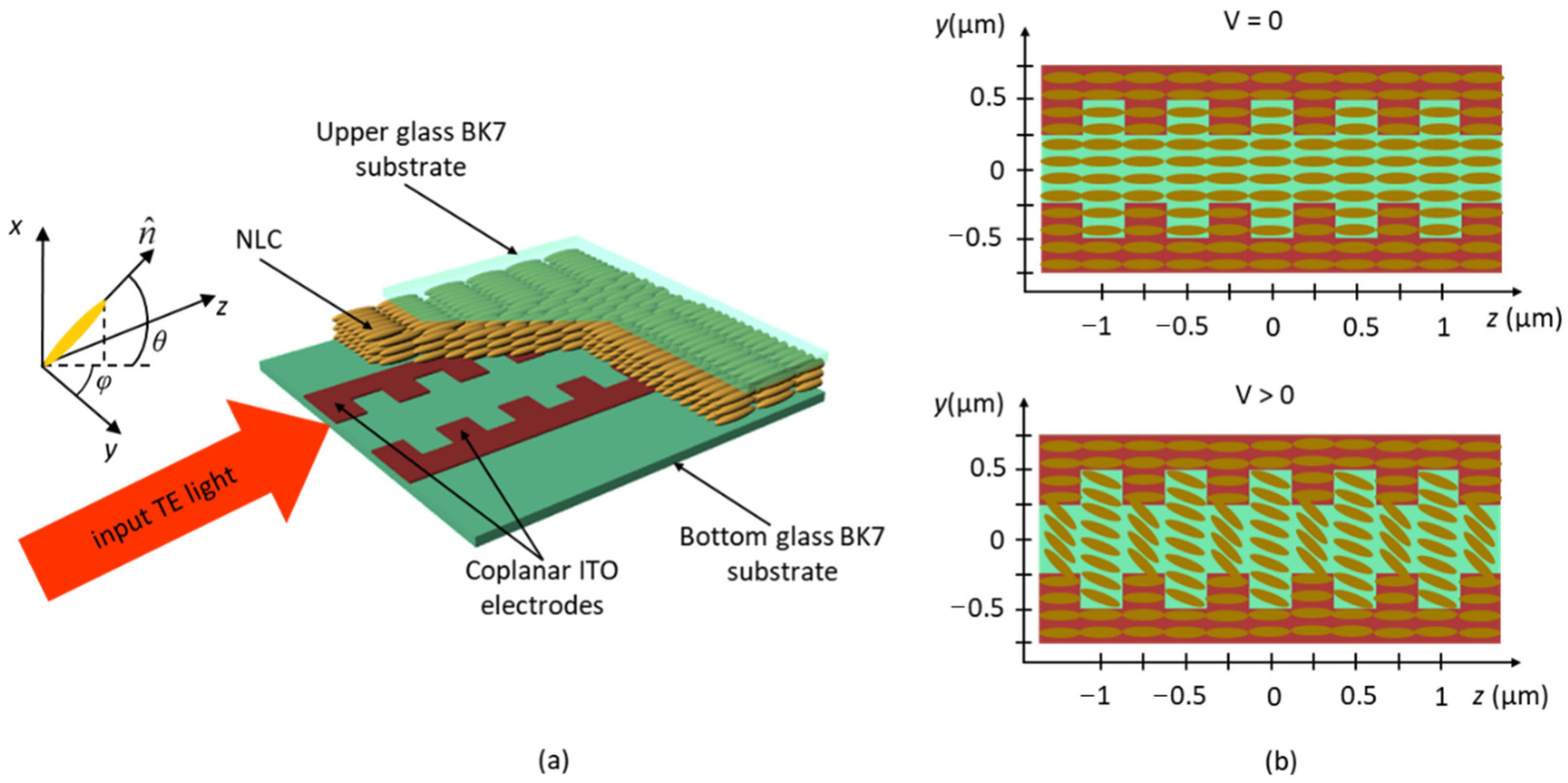
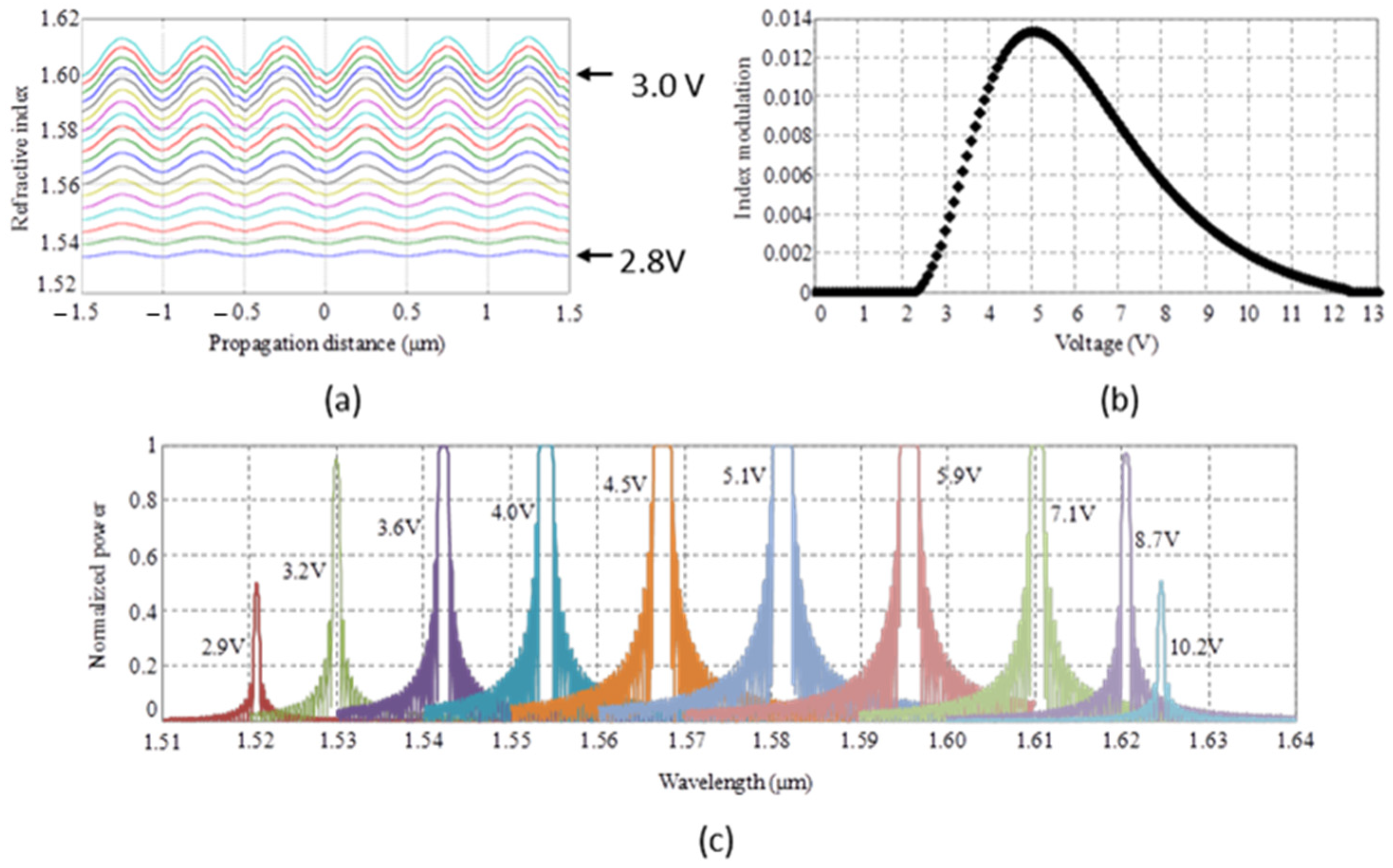
4.3. Nematic LC Electrically Tunable Bragg Reflectors

Tunable Bragg reflector structures based on an LC waveguide between two glass plates have been demonstrated, where the peak reflection wavelength tuning is driven electro-optically by modifying the LC refractive index [64,65]. Hereinafter, relying on the same physical model, two possible arrangements of electrodes are reported: a top–bottom electrode disposition and a coplanar electrode configuration. The working principle is based on a refractive index modulation to obtain a Bragg grating along the propagation direction, which allows a wavelength-selective propagation of an optical signal inside the LC layer. Estimation of the reorientation of the LC molecular director has been evaluated as described in Section 2 by considering only an elastic term and an electrostatic term in the expression of F. Coupled mode theory was used for both configurations to evaluate both resonant Bragg wavelength and back-reflected power for TM or TE polarized input light at a specific grating length. A wide wavelength tuning range and a high wavelength selectivity can be achieved in both structures through application of low voltages.
The configuration of the Bragg reflector device based on top–bottom electrodes to obtain an electro-optic distributed feedback waveguide (DFBW) with full adjustability of confinement and Bragg resonance wavelength is shown in Figure 17 [66]. It consists of a planar glass cell with a nematic LC layer and a top–bottom configuration of transparent electrodes allowing an external voltage application. LC molecules are arranged with a planar alignment with the director n parallel to the propagation direction. Two-dimensional optical confinement of propagating transverse-magnetic TM light polarization is ensured through a graded-index channel by a suitable voltage applied between the comb-shaped top electrode periodic along the propagation direction and the ground plane at the opposite boundary.
A Bragg grating can be induced through LC refractive index modulation over a finite propagation distance and for a given operation wavelength to allow a one-dimensional photonic lattice entailing Bragg reflection via distributed feedback. The structure can be optimized in terms of electrode dimensions, periodicity and duty-cycle along the propagation direction and the LC layer thickness to meet the required operation mode as wavelength-selective reflector and tunable drop-multiplexer.
Modulation of the refractive index 100 nm below the top electrode experienced by the TM00 mode versus propagation distance or applied voltages from 2 to 3 V (in 0.2 V steps) is reported in Figure 18a. As reported in Figure 18b, a wavelength tuning of 14 nm (1536–1550 nm) is achievable with applied voltages ranging from 2.5 V to 3 V (further details on technology parameters can be found in ref [66]).
Another structure of LC tuneable Bragg reflector with a coplanar electrode configuration has been investigated and demonstrated allowing a wavelength tuning range of more than 100 nm in the near infrared with about 10 V applied [67]. Figure 19a is a schematic three-dimensional view of the device.
The arrangement is made with a nematic LC planar waveguide restrained between two parallel glass slides. A pair of coplanar comb-shaped 100 nm thick ITO transparent electrodes are deposited and patterned on the inner face of the bottom substrate periodically positioned along the propagation direction. The nematic LC molecules lie with their director aligned along the propagation direction when no voltage is applied, while the field arising when a voltage is applied induces the LC molecular reorientation in the longitudinal plane, resulting in a pure twist deformation that finally leads to a bidimensional optical confinement of the propagating TE polarized beam in the xy plane, as shown in Figure 19b. In Figure 20a, the sinusoidal behaviour of the refractive index modulation achieved along the direction propagation is plotted, corresponding to a phase grating for distributed feedback.
The resulting index contrast versus voltage between 0 and 13 V is reported in Figure 20b. The nematic LC reorientation effect is almost negligible up to 2.4 V, leading to little index modulation, but this changes rapidly after this threshold: at V = 5 V, the nematic LC molecules are completely reoriented, reaching their maximum twist ϕ = 90°. Further voltage increase allows LC reorientation which also occurs in the regions that have not yet been completely reoriented, yielding a decrease in modulation. Above 12.4 V, almost all the nematic LC molecules are reoriented parallel to y, and the index contrast is zero.
The back-reflected power (spectral reflectivity) as a function of the resonant wavelength for a device length of 1.5 mm, corresponding to 3000 periods, is reported in Figure 20c. A wide tuning range of 104 nm (1521–1625 nm) can be obtained by varying the applied voltage between 2.9 and 10.2 V, keeping the back-reflection above 50%, with a good spectral selectivity.

5. Conclusions

LC materials can be successfully used beyond the well-known FPD applications. Superb linear and nonlinear optical properties of LC materials have been deeply explored to make a wide range of integrated optic devices. Optical waveguides with an electro-optically or all-optically controlled core enable the development of many integrated optic devices which can be driven by sub-milliwatt signals. Straightforward modelling allows to design simulate several photonic functions, such as switching and filtering and light generation. In this paper, a few examples of photonic devices either for optical switching with extinction ratios over 40 dB, or for optical filtering over 100 nm tuning range have been reported to demonstrate the great LC application potentialities in integrated optics for optical communications and optical sensing systems with low power consumptions. Innovative integrated photonic devices based on LC include combinations of LC with metal nanoparticles for novel sensing systems based on photothermal therapies. Further research could be devoted to the development of integrated optic devices for 3D sensing, augmented reality, terahertz communication and terahertz imaging. The generated vortex beam via q-plates of LCs and vortex gratings could help in studying the interaction of spin-orbital angular momentum for quantum information applications.

Author Contributions

Conceptualization, A.d. and R.A.; methodology, A.d.; software, R.A.; validation, A.d. and R.A.; investigation, A.d. and R.A.; data curation, A.d. and R.A.; writing—original draft preparation, A.d. and R.A.; writing—review and editing, A.d. and R.A.; supervision, A.d. and R.A.; funding acquisition, A.d. and R.A. All authors have read and agreed to the published version of the manuscript.

Funding

This research received no external funding.

Conflicts of Interest

The authors declare no conflict of interest.

References

  1. Khoo, I.C. Liquid Crystals, 2nd ed.; Wiley: New York, NY, USA, 2007. [Google Scholar]
  2. Zografopoulos, D.C.; Asquini, R.; Kriezis, E.; D’Alessandro, A.; Beccherelli, R. Guided-wave liquid-crystal photonics. Lab A Chip 2012, 12, 3598–3610. [Google Scholar] [CrossRef]
  3. Beeckman, J.; Neyts, K.; Vanbrabant, P.J.M. Liquid-crystal photonic applications. Opt. Eng. 2011, 50, 081202. [Google Scholar] [CrossRef] [Green Version]
  4. Donisi, D.; Bellini, B.; Beccherelli, R.; Asquini, R.; Gilardi, G.; Trotta, M.; D’Alessandro, A. A Switchable Liquid-Crystal Optical Channel Waveguide on Silicon. IEEE J. Quantum Electron. 2010, 46, 762–768. [Google Scholar] [CrossRef]
  5. d’Alessandro, A.; Asquini, R.; Trotta, M.; Gilardi, G.; Beccherelli, R.; Khoo, I.C. All-optical intensity modulation of near infrared light in a liquid crystal channel waveguide. Appl. Phys. Lett. 2010, 97, 093302. [Google Scholar] [CrossRef]
  6. Neyts, G.K.; Beeckman, J.; Desmet, H. Waveguiding with liquid crystals. Proc. SPIE 2007, 6487, 64870O. [Google Scholar]
  7. Scalia, G.; Hermann, D.S.; Abbate, G.; Komitov, L.; Mormile, P.; Righini, G.C.; Sirleto, L. Integrated Electro-Optic Switch Based on a Ferroelectric Liquid Crystal Waveguide. Mol. Cryst. Liq. Cryst. 1998, 320, 321–335. [Google Scholar] [CrossRef]
  8. d’Alessandro, A.; Bellini, B.; Donisi, D.; Beccherelli, R.; Asquini, R. Nematic liquid crystal optical channel waveguides on silicon. IEEE J. Quant. Electron. 2006, 42, 1084–1090. [Google Scholar] [CrossRef]
  9. Peddireddy, K.; Jampani, V.S.R.; Thutupalli, S.; Herminghaus, S.; Bahr, C.; Muševič, I. Lasing and waveguiding in smectic A liquid crystal optical fibers. Opt. Express 2013, 21, 30233–30242. [Google Scholar] [CrossRef]
  10. Čančula, M.; Ravnik, M.; Muševič, I.; Žumer, S. Liquid microlenses and waveguides from bulk nematic birefringent profiles. Opt. Express 2016, 19, 22177–22188. [Google Scholar] [CrossRef]
  11. Xing, Y.; Ako, T.; George, J.P.; Korn, D.; Yu, H.; Verheyen, P.; Pantouvaki, M.; Lepage, G.; Absil, P.; Ruocco Koos, C.; et al. Digitally Controlled Phase Shifter Using an SOI Slot Waveguide with Liquid Crystal Infiltration. IEEE Photon. Technol. Lett. 2015, 27, 1269–1272. [Google Scholar] [CrossRef]
  12. Wang, T.-J.; Chaung, C.-K.; Li, W.-J.; Chen, T.-J.; Chen, B.-Y. Electrically Tunable Liquid-Crystal-Core Optical Channel Waveguide. J. Light. Technol. 2013, 31, 3570–3574. [Google Scholar] [CrossRef]
  13. Li, J.; Chu, D. Liquid Crystal-Based Enclosed Coplanar Waveguide Phase Shifter for 54–66 GHz Applications. Crystals 2019, 9, 650. [Google Scholar] [CrossRef] [Green Version]
  14. Reese, R.; Polat, E.; Tesmer HStrobl, J.; Schuster, C.; Nickel, M.; Granja, A.B.; Jakoby, R.; Maune, H. Liquid Crystal Based Dielectric Waveguide Phase Shifters for Phased Arrays at W-Band. IEEE Access 2019, 7, 127032–127041. [Google Scholar] [CrossRef]
  15. Tripathi, U.S.; Rastogi, V. Liquid Crystal Based Rib Waveguide. J. Lightw. Technol. 2020, 38, 4045–4051. [Google Scholar] [CrossRef]
  16. Assanto, G.; Peccianti, M.; Conti, C. Nematicons: Optical Spatial Solitons in Nematic Liquid Crystals. Opt. Photon-News 2003, 14, 44–48. [Google Scholar] [CrossRef]
  17. Henninot, J.-F.; Blach, J.-F.; Warenghem, M. Experimental study of the nonlocality of spatial optical solitons excited in nematic liquid crystal. J. Opt. A Pure Appl. Opt. 2007, 9, 20–25. [Google Scholar] [CrossRef]
  18. Assanto, G.; Fratalocchi, A.; Peccianti, M. Spatial solitons in nematic liquid crystals. Opt. Exp. 2007, 15, 5248–5259. [Google Scholar] [CrossRef]
  19. Piccardi, A.; Alberucci, A.; Bortolozzo, U.; Residori, S.; Assanto, G. Soliton gating and switching in liquid crystal light valve. Appl. Phys. Lett. 2010, 96, 071104. [Google Scholar] [CrossRef]
  20. Piccardi, A.; Trotta, M.; Kwasny, M.; Alberucci, A.; Asquini, R.; Karpierz, M.; D’Alessandro, A.; Assanto, G. Trends and trade-offs in nematicon propagation. Appl. Phys. A 2011, 104, 805–811. [Google Scholar] [CrossRef]
  21. Jung, P.S.; Krolikowski, W.; Laudyn, U.A.; Trippenbach, M.; Karpierz, M. Supermode spatial optical solitons in liquid crystals with competing nonlinearities. Phys. Rev. A 2017, 95, 023820. [Google Scholar] [CrossRef] [Green Version]
  22. Aya, S.; Araoka, F. Kinetics of motile solitons in nematic liquid crystals. Nat. Commun. 2020, 11, 3248. [Google Scholar] [CrossRef] [PubMed]
  23. Du, F.; Lu, Y.-Q.; Wu, S.-T. Electrically tunable liquid-crystal photonic crystal fiber. Appl. Phys. Lett. 2004, 85, 2181–2183. [Google Scholar] [CrossRef] [Green Version]
  24. Woliński, T.; Ertman, S.; Lesiak, P.; Domański, A.; Czapla, A.; Dąbrowski, R.; Nowinowski-Kruszelnicki, E.; Wójcik, J. Photonic liquid crystal fibers—A new challenge for fiber optics and liquid crystals photonics. Opto-Electron. Rev. 2006, 14, 329–334. [Google Scholar] [CrossRef]
  25. Lee, C.; Chen, C.; Kao, C.; Yu, C.; Yeh, S.; Cheng, W.; Lin, T. Photo and electrical tunable effects in photonic liquid crystal fiber. Opt. Express 2010, 18, 2814–2821. [Google Scholar] [CrossRef] [PubMed]
  26. Lorenz, A.; Kitzerow, H.-S. Efficient electro-optic switching in a photonic liquid crystal fiber. Appl. Phys. Lett. 2011, 98, 241106. [Google Scholar] [CrossRef]
  27. Budaszewski, D.; Chychłowski, M.; Budaszewska, A.; Bartosewicz, B.; Jankiewicz, B.; Wolinski, T. Enhanced efficiency of electric field tunability in photonic liquid crystal fibers doped with gold nanoparticles. Opt. Express 2019, 27, 14260–14269. [Google Scholar] [CrossRef] [PubMed]
  28. Vasdekis, A.; Cuennet, J.G.; Psaltis, D. Liquid crystal optofluidics. Proc. SPIE 2012, 847507. [Google Scholar] [CrossRef]
  29. De Sio, L.; Romito, M.; Giocondo, M.; Vasdekis, A.; De Luca, A.; Umeton, C. Electro-switchable polydimethylsiloxane-based optofluidics. Lab A Chip 2012, 12, 3760–3765. [Google Scholar] [CrossRef]
  30. Cuennet, J.G.; Vasdekis, A.E.; Psaltis, D. Optofluidic-tunable color filters and spectroscopy based on liquid-crystal microflows. Lab Chip 2013, 13, 2721–2726. [Google Scholar] [CrossRef] [Green Version]
  31. d’Alessandro, A.; Martini, L.; Gilardi, G.; Beccherelli, R.; Asquini, R. Polarization-Independent Nematic Liquid Crystal Waveguides for Optofluidic Applications. IEEE Photonics Technol. Lett. 2015, 27, 1709–1712. [Google Scholar] [CrossRef]
  32. Čopar, S.; Kos, Ž.; Emeršič, T.; Tkalec, U. Microfluidic control over topological states in channel-confined nematic flows. Nat. Commun. 2020, 11, 59. [Google Scholar] [CrossRef] [PubMed]
  33. Ramaniuk, A.; Jung, P.S.; Christodoulides, D.N.; Krolikowski, W.; Trippenbach, M. Absorption-mediated stabilization of nonlinear propagation of vortex beams in nematic liquid crystals. Opt. Commun. 2019, 451, 338–344. [Google Scholar] [CrossRef]
  34. Laudyn, U.A.; Kwaśny, M.; Karpierz, M.A.; Assanto, G. Vortex nematicons in planar cells. Opt. Express 2020, 28, 8282–8290. [Google Scholar] [CrossRef] [PubMed]
  35. Jung, P.S.; Krolikowski, W.; Laudyn, U.A.; Karpierz, M.A.; Trippenbach, M. Semi-analytical approach to supermode spatial solitons formation in nematic liquid crystals. Opt. Express 2017, 25, 23893–23898. [Google Scholar] [CrossRef] [PubMed]
  36. Ramaniuk, A.; Trippenbach, M.; Jung, P.S.; Christodoulides, D.N.; Krolikowski, W.; Assanto, G. Scalar and vector su-permode solitons owing to competing nonlocal nonlinearities. Opt. Express 2021, 29, 8015–8023. [Google Scholar] [CrossRef]
  37. Piccirillo, B.; Toscano, C.; Vetrano, F.; Santamato, E. Orbital and Spin Photon Angular Momentum Transfer in Liquid Crystals. Phys. Rev. Lett. 2001, 86, 2285. [Google Scholar] [CrossRef]
  38. Slussarenko, S.; Murauski, A.; Du, T.; Chigrinov, V.; Marrucci, L.; Santamato, E. Tunable liquid crystal q-plates with arbitrary topological charge. Opt. Express 2011, 19, 4085–4090. [Google Scholar] [CrossRef] [PubMed] [Green Version]
  39. Keum, C.; Liu, S.; Al-Shadeedi, A.; Kaphle, V.; Callens, M.K.; Han, L.; Neyts, K.; Zhao, H.; Gather, M.C.; Bunge, S.D.; et al. Tuning charge carrier transport and optical birefringence in liquid-crystalline thin films: A new design space for organic light-emitting diodes. Sci. Rep. 2018, 8, 699. [Google Scholar] [CrossRef] [Green Version]
  40. Lei, X.; Wieschendorf, C.; Firth, J.; Ladouceur, F.; Fuerbach, A.; Silvestri, L. Numerical modelling and optimization of actively Q-switched waveguide lasers based on liquid crystal transducers. Opt. Express 2019, 27, 8777–8791. [Google Scholar] [CrossRef]
  41. Belmonte, C.; Frasunkiewicz, L.; Czyszanowski, T.; Thienpont, H.; Beeckman, J.; Neyts, K.; Panajotov, K. Optimization of electrically tunable VCSEL with intracavity nematic liquid crystal. Opt. Express 2015, 23, 15706–15715. [Google Scholar] [CrossRef] [Green Version]
  42. Pfeifle, J.; Alloatti, L.; Freude, W.; Leuthold, J.; Koos, C. Silicon-organic hybrid phase shifter based on a slot waveguide with a liquid-crystal cladding. Opt. Express 2012, 20, 15359–15376. [Google Scholar] [CrossRef]
  43. Henninot, J.F.; Debailleul, M.; Asquini, R.; d’Alessandro, A.; Warenghem, M. Self-waveguiding in an isotropic channel induced in dye doped nematic liquid crystal and a bent self-waveguide. J. Opt. A: Pure Appl. Opt. 2004, 6, 315–323. [Google Scholar] [CrossRef]
  44. Bellini, B.; Larchanché, J.-F.; Vilcot, J.-P.; DeCoster, D.; Beccherelli, R.; D’Alessandro, A. Photonic devices based on preferential etching. Appl. Opt. 2005, 44, 7181–7186. [Google Scholar] [CrossRef] [PubMed]
  45. Bellini, B.; d’Alessandro, A.; Beccherelli, R. A method for butt-coupling optical fibers to liquid crystal planar waveguides. Opt. Mater. 2007, 29, 1019–1022. [Google Scholar] [CrossRef]
  46. Chigrinov, V.G.; Kozenkov, V.M.; Kwok, H.-S. Photoalignment of Liquid Crystalline Materials: Physics and Applications; Wiley: New York, NY, USA, 2008. [Google Scholar]
  47. Schadt, M. Liquid creystal displays, LC materials and LPP photoalignment. Mol. Cryst. Liq. Cryst. 2017, 320, 253–268. [Google Scholar] [CrossRef] [Green Version]
  48. Duffy, D.C.; McDonald, J.C.; Schueller, O.J.A.; Whitesides, G.M. Rapid Prototyping of Microfluidic Systems in Poly(dimethylsiloxane). Anal. Chem. 1998, 70, 4974–4984. [Google Scholar] [CrossRef] [PubMed]
  49. Lee, L.-H. Enhancement of surface wettability of adhesive silicone rubber by oxidation. J. Adhes. 1972, 4, 39–49. [Google Scholar] [CrossRef]
  50. Du, P.; Lin, X.; Zhang, X. Dielectric constants of PDMS nanocomposites using conducting polymer nanowires. In Proceedings of the 16th International Solid-State Sensors, Actuators and Microsystems Conference, Beijing, China, 5–9 June 2011; pp. 645–648. [Google Scholar]
  51. Wang, Z.; Volinsky, A.A.; Gallant, N.D. Crosslinking effect on polydimethylsiloxane elastic modulus measured by custom-built compression instrument. J. Appl. Polym. Sci. 2014, 131, 41050. [Google Scholar] [CrossRef] [Green Version]
  52. McDonald, J.C.; Duffy, D.C.; Anderson, J.R.; Chiu, D.T.; Wu, H.; Schueller, O.J.; Whitesides, G.M. Fabrication of microfluidic systems in poly(dimethylsiloxane). Electrophoresis 2000, 21, 27–40. [Google Scholar] [CrossRef]
  53. Missinne, J.; Kalathimekkad, S.; Van Hoe, B.; Bosman, E.; Vanfleteren, J.; Van Steenberge, G. Stretchable optical waveguides. Opt. Express 2014, 22, 4168–4179. [Google Scholar] [CrossRef] [Green Version]
  54. Yeh, P.; Gu, C. Optics of Liquid Crystal Displays; Wiley: New York, NY, USA, 1999. [Google Scholar]
  55. Lebwohl, P.A.; Lasher, G. Nematic-Liquid-Crystal Order—A Monte Carlo Calculation. Phys. Rev. A 1972, 6, 426–429. [Google Scholar] [CrossRef]
  56. Pasini, P.; Chiccoli, C.; Zannoni, C. Advances in the Computer Simulations of Liquid Crystals; Kluwer: Dordrecht, Germany, 2000. [Google Scholar]
  57. D’Alessandro, A.; Asquini, R.; Chiccoli, C.; Pasini, P.; Zannoni, C. Liquid crystal channel waveguides: A computer simulation of the application of transversal external fields. Mol. Cryst. Liq. Cryst. 2017, 649, 79–85. [Google Scholar] [CrossRef]
  58. d’Alessandro, A.; D’Orazio, A.; Campoli, F.; Petruzzelli, V.; Chessa, G.; Maltese, P. Design of an Ultrashort Directional Coupler with an SSFLC Coupling Layer. Mol. Cryst. Liq. Cryst. 1998, 320, 355–364. [Google Scholar] [CrossRef]
  59. Asquini, R.; D’Alessandro, A. BPM Analysis of an Integrated Optical Switch using Polymeric Optical Waveguides and SSFLC at 1.55 µm. Mol. Cryst. Liq. Cryst. 2002, 375, 243–251. [Google Scholar] [CrossRef]
  60. Vanbrabant, P.J.M.; Beeckman, J.; Neyts, K.; James, R.; Fernandez, F.A. A finite element beam propagation method for simulation of liquid crystal devices. Opt. Express 2009, 17, 10895–10909. [Google Scholar] [CrossRef] [PubMed]
  61. Asquini, R.; Fratalocchi, A.; D’Alessandro, A.; Assanto, G. Electro-optic routing in a nematic liquid-crystal waveguide. Appl. Opt. 2005, 44, 4136–4143. [Google Scholar] [CrossRef] [PubMed]
  62. Fratalocchi, A.; Asquini, R.; Assanto, G. Integrated electro-optic switch in liquid crystals. Opt. Express 2005, 13, 32–37. [Google Scholar] [CrossRef]
  63. Asquini, R.; Chiccoli, C.; Pasini, P.; Civita, L.; D’Alessandro, A. Low power photonic devices based on electrically controlled nematic liquid crystals embedded in poly (dimethylsiloxane). Liq. Cryst. 2018, 45, 2174–2183. [Google Scholar] [CrossRef]
  64. Asquini, R.; Gilardi, G.; D’Alessandro, A.; Assanto, G. Integrated Bragg reflectors in low-index media: Enabling strategies for wavelength tunability in electro-optic liquid crystals. Opt. Eng. 2011, 50, 71108. [Google Scholar] [CrossRef]
  65. Asquini, R.; D’Alessandro, A. Tunable photonic devices based on liquid crystals and composites. Proc. SPIE 2013, 8828, 88280T. [Google Scholar] [CrossRef]
  66. Donisi, D.; Asquini, R.; d’Alessandro, A.; Assanto, G. Distributed feedback grating in liquid crystal waveguide: A novel approach. Opt. Express 2009, 17, 5251–5256. [Google Scholar] [CrossRef] [PubMed]
  67. Gilardi, G.; Asquini, R.; d’Alessandro, A.; Assanto, G. Widely tunable electro-optic distributed Bragg reflector in liquid crystal waveguide. Opt. Express 2010, 18, 11524–11529. [Google Scholar] [CrossRef] [PubMed]
Figure 1. Schematic molecular structure of thermotropic LCs.
Applsci 11 08713 g001
Figure 2. Optical waveguide made of LC infiltrated in a SiO2/Si V-groove: (a) Three-dimensional exploded schematic, showing the orientation of the nematic LC molecules along the V-groove; (b) Electron microscope scanning of a SiO2/Si V-groove.
Applsci 11 08713 g002
Figure 3. Schematic images of an LC waveguide in SiO2/Si groove: (a) cross-section indicating the etching angle of the Si groove; (b) longitudinal section showing the orientation of the nematic LC molecules under applied electric field between ITO and n-Si.
Applsci 11 08713 g003
Figure 4. Picture of a single-mode optical fiber which is butt-coupled to a chip, including a set of LC waveguides on SiO2/Si grooves. Waveguide width is 8–12 µm.
Applsci 11 08713 g004
Figure 5. Technological phases to make PDMS microchannels used obtain LC:PDMS waveguides.
Applsci 11 08713 g005
Figure 6. LC:PDMS waveguides: (a) oriented LC molecules inside the PDMS channel; (b) PDMS chip with optical waveguides with widths of 8, 10 and 15 µm; (c) image of LC:PDMS waveguides with a width of 10 µm observed under the microscope in transmission.
Applsci 11 08713 g006
Figure 7. Propagation properties of an LC:PDMS waveguide with a width of 15 µm: (a) green laser light (wavelength = 532 nm) beam butt−coupled by using a single mode optical fiber of 125 µm; (b) output power versus polarization at a wavelength of 1550 nm.
Applsci 11 08713 g007
Figure 8. Molecular director n and refractive index at the molecular level.
Applsci 11 08713 g008
Figure 9. Computed all-optical dependence of the refractive index distribution in a SiO2/Si LCW with upper width of 10 µm: (a) without input optical signal; (b) with input optical signal.
Applsci 11 08713 g009
Figure 10. Computed contour map of TM-like propagation of 1550 nm wavelength in a 10 µm wide LCW with applied lines of electric field force (red arrows) for an applied voltage of 10 V: (a) fundamental mode; (b) higher order mode. The color maps show the field intensity distribution.
Applsci 11 08713 g010
Figure 11. Operation of a SiO2/Si groove LCW, with an electric field applied between n-Si substrate and an ITO layer: (a) case of no external voltage applied; (b) case of voltage above threshold to tilt LC molecules which allows light propagation. Reprinted with permission from Ref. [4]. Copyright 2010 IEEE.
Applsci 11 08713 g011
Figure 12. Plot of the extinction ratio (ER) as a function of the applied voltage for a SiO2/Si LCW.
Applsci 11 08713 g012
Figure 13. Electro-optic router: (a) three-dimensional view; (b) side view; (c) top view.
Applsci 11 08713 g013
Figure 14. Image of the field distribution due to two superimposed TM guided modes in a 1 × 2 optical switch encompassing an output Y-junction.
Applsci 11 08713 g014
Figure 15. LC guided−wave electro−optic router light propagation in the (y; z) plane: (a) V = Vl = 0.98 V; (b) V = Vh = 1.19 V; (c) corresponding output intensity distributions.
Applsci 11 08713 g015
Figure 16. LC:PDMS zero−gap directional coupler switch with bimodal central waveguide and coplanar electrodes: (a) device top view; (b) cross-section of the bimodal LC waveguide.
Applsci 11 08713 g016
Figure 17. Tunable Bragg reflector with top–bottom electrode configuration with planarly anchored nematic LC.
Applsci 11 08713 g017
Figure 18. Tuning characteristics of the nematic LC tunable Bragg reflector with top–bottom electrode configuration: (a) refractive index profile modulation along propagation direction for applied voltages between 2 V (bottom line) and 3 V (top line) in 0.2 V steps; (b) normalized grating reflectivity for 2.5 V (red), 2.8 V (green) and 3 V (blue). Reprinted with permission from Ref. [66]. Copyright 2009 OSA.
Applsci 11 08713 g018
Figure 19. Tunable Bragg reflector with coplanar electrode configuration and planarly anchored nematic LC: (a) three-dimensional view; (b) molecular orientation above the electrodes without (V = 0) and with (V > 0) applied electric field.
Applsci 11 08713 g019
Figure 20. Performance of a tunable Bragg reflector with coplanar electrode configuration: (a) refractive index modulation along the propagation direction for applied voltages between 2.8 V (bottom line) and 3 V (top line); (b) longitudinal modulation versus applied voltage; (c) spectral reflectivity for propagation over 1.5 mm (3000 periods) and for different voltages. Reprinted with permission from Ref. [67]. Copyright 2010 OSA.
Applsci 11 08713 g020
Publisher’s Note: MDPI stays neutral with regard to jurisdictional claims in published maps and institutional affiliations.

