Article

Portable and Highly Versatile Impedance Meter for Very Low Frequency Measurements

Dipartimento di Ingegneria, University of Messina, 98166 Messina, Italy
*
Author to whom correspondence should be addressed.
Appl. Sci. 2021, 11(17), 8234; https://doi.org/10.3390/app11178234
Submission received: 30 July 2021 / Revised: 24 August 2021 / Accepted: 1 September 2021 / Published: 5 September 2021

Abstract

:
Electrical Impedance Spectroscopy (EIS) is a characterization technique that is gaining more and more importance in various fields of research and applications. The frequency range of investigation varies according to the type of application. In some fields (biology, medicine, energy) it is useful to be able to perform measurements at very low frequency values (down to a few mHz or even below). While impedance meters operating at frequencies in the range from a few tens of Hz up to a few MHz can be regarded as quite standard pieces of instrumentation commonly available in many laboratories, instrumentation for measurements at very low frequencies, although commercially available, is less common. The subject of this work is the design, realization and testing of a low frequency impedance measurement platform that has the advantage of being portable, rather inexpensive, and yet highly versatile. In our approach, we exploit a personal computer and a soundboard as a powerful system for digital signal generation and analysis that, with the help of low complexity and low-cost external hardware and a public domain software for the implementation of the core system, allow to tailor the platform for targeting specific applications with minimal effort. As an example, we will demonstrate the application of the system to the investigation of polypyrrole-based supercapacitor structures.

1. Introduction

Electrical Impedance Spectroscopy (EIS) is a non-invasive testing technique that has been extensively used and applied in several research fields. In medicine, for example, EIS (or BIS, Biological Impedance Spectroscopy) has proven to be an effective technique for non-invasive analyses and diagnosis of the healthy condition of subjects in a few medical fields [1,2,3,4,5,6,7,8] and furthermore, it seems to be appropriate for the characterization of the physicochemical properties of pharmaceutical materials [9] and of bacteria [10,11,12] and viruses [13,14].
The complex impedance of biological tissues exhibits different behaviors as the frequency varies in a very wide range [15] and different phenomena have been recognized, which are responsible for such variations [16]. Although it is well established that these variations of behavior occur from frequencies close to dc up to frequencies in the order of MHz (and, in some cases, GHz), the frequency range of 10 kHz–100 kHz has been considered the most suitable for BIS measurements [17,18,19,20] and the frequency of 50 kHz [21] has often been chosen for data interpretation. Other researchers have lowered the minimum investigation frequency to 100 Hz [22,23]. This implies that bio-impedance measurements have so far neglected the effects due to the so-called α dispersion [16], which takes into account the relaxation of ions surrounding the charged cellular membrane and which dominates the impedance behavior from 0 Hz to a few hundred Hertz.
Although the results obtained at higher frequencies can be in some cases regarded as reliable and satisfactory, one cannot fail to consider that without measurements in the very low-frequency range the characterization is incomplete and important, and useful information might be possibly missed [24]. Therefore, having an instrument capable of carrying out very low frequency impedance measurements would be useful in the field of bioengineering. This is however true also in other fields. EIS is also used for the characterization of the electrochemical behavior of energy storage devices and electrode materials for supercapacitors, batteries and fuel cells [25,26,27,28]. As in the case of medical and biological applications, also in these applications the elements to be characterized are modeled by means of multi-element models. As a consequence, the impedance measurements have to be performed in a wide frequency range and, also in these cases, down to very low frequencies, extending in some cases below 1 mHz [29].
In the worldwide market, impedance analyzers with very good performances and capable of performing measurements of this type are available (Solartron, Novocontrol, Zahner, Hioki, CorrTest) [30,31,32,33,34], but this kind of general-purpose instrumentation is characterized by high complexity and, inevitably, high costs.
On the basis of these considerations, our work has been focused on the realization of a low-cost and yet high versatile hardware platform for the development of low frequency impedance measurement applications. In designing the system, we regarded the ability to easily reproduce it as the most important feature to be achieved, so that any researcher can take advantage of its potentialities in any given field of application. For this reason, we have sacrificed a high degree of automation for simplicity, so that some of the adjustments required for the optimization of the sensitivity depending on the characteristics of the Device Under Test (DUT) have to be done by manually changing a few key components in the system, via a snap-in/snap-out approach. Moreover, the system is highly modular so that one can take advantage of the core components while designing a dedicated front end for specific applications. At the same time, since capacitive parasitic components are not the main concern at very low frequencies, high configurability can be easily implemented by resorting to low-cost switch matrices controlled by a personal computer. To obtain high sensitivity and a high degree of flexibility in signal elaboration, the system is based on a commercial Audio Board (AB) and on a Personal Computer (PC) for signal generation/acquisition and digital signal elaboration, respectively. The key external components are the hardware required to allow the inputs and outputs of the Audio Board to interface to low frequency signals (down to DC) and the front end for interfacing to the DUT. Typically, different front ends can be designed in order to accommodate different requirements in terms of voltage levels (DC bias level and AC bias amplitudes) and/or supplied current to the DUT. The core software subsystem is either based on a public domain library or developed and made freely available by the authors, so that anyone, besides easily reproducing the prototype that will be discussed in this paper, can design his/her own customized system based on the approach we propose.
The rest of the paper is organized as stated in the following. In Section 2 and Section 3 the hardware and the software components of the design are described, respectively. In Section 4 a few test measurements are reported.

2. Materials and Methods

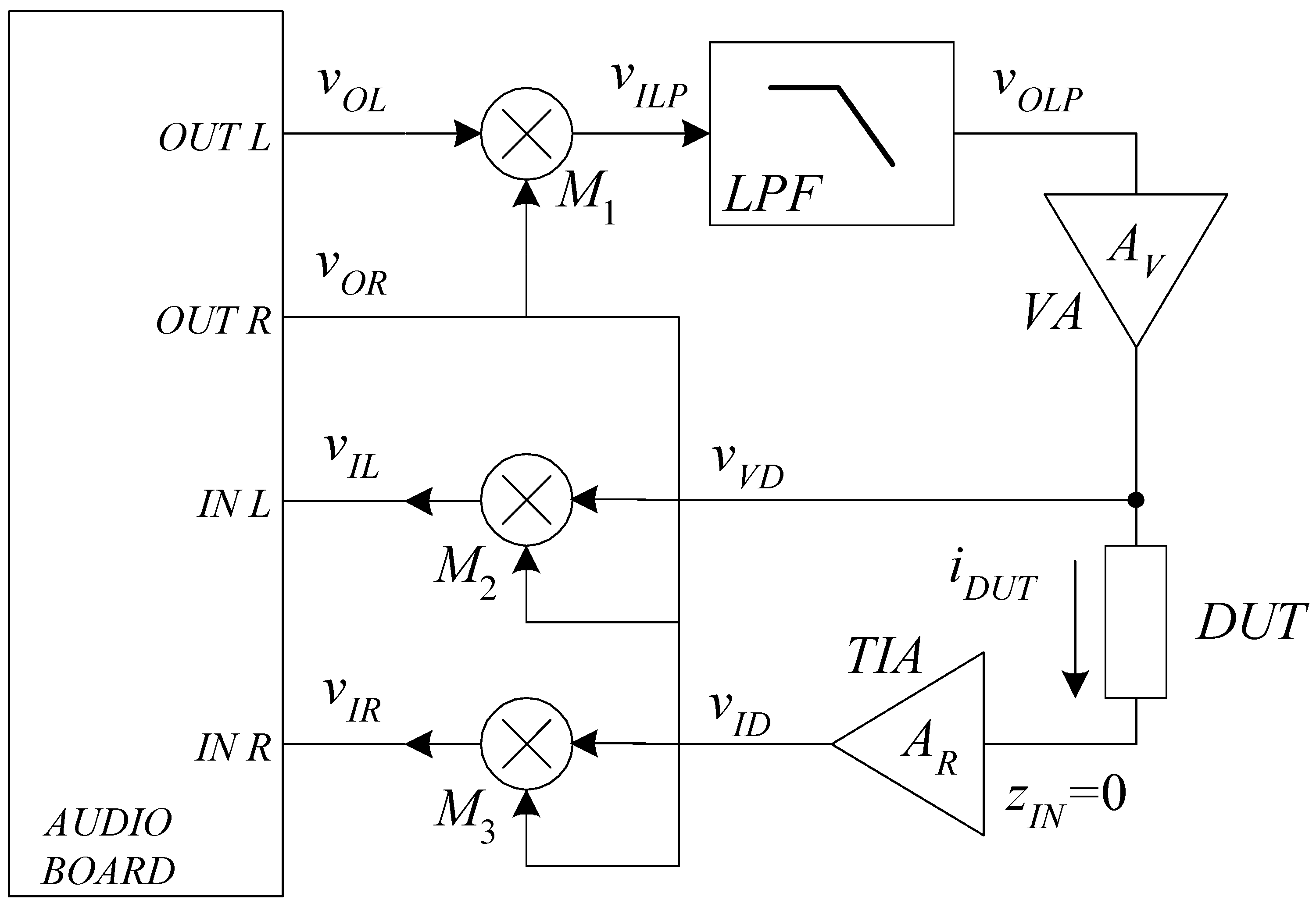
2.1. Principle of Operation

In approaching the design of an impedance meter to be used for the characterization of devices and materials in the frequency range from a few tens of mHz up to a few hundred Hz, we regarded low hardware complexity and high versatility as the most important goals to be obtained. By reducing the hardware complexity, the system can be more easily reproduced by researchers interested in its application. This is why we investigated in the first place the possibility of resorting to a standard audio board for signal generation and acquisition with a personal computer acting as a powerful platform for digital signal elaboration. While the modern audio board can have impressive performances in terms of resolution (24-bit resolution is common in many modern low to mid-range devices), due to AC coupling they cannot directly generate and acquire signals with frequencies below a few Hz. This problem, however, can be quite easily addressed and solved by resorting to simple modulation/demodulation operations as illustrated in Figure 1. Let us assume that the audio board is configured to work with a standard sampling frequency of 48 kHz and a resolution of 24 bits. One of the outputs of the audio board (OUT R) is used to generate a sinusoidal signal with constant amplitude AC and constant frequency fC:
v O R = A C cos ( 2 π f C t )
This signal vOR is used as a carrier for synchronous demodulation/modulation and it reaches the inputs of all three analog multipliers M1, M2, M3 in Figure 1. Typically, AC is set at the maximum value compatible with the input dynamic of the multipliers. The frequency fC is chosen to be very large in comparison with the test frequencies to be delivered to the Device Under Test (DUT), but well within the passband of the audio board. Typically, fC is in the order of 10 kHz. The second output of the audio board (OUT L) is used to generate a signal that, when multiplied by vOR and filtered by the Low Pass Filter (LPF) results in a low frequency sinusoidal signal, possibly superimposed to a DC level, at the output vOLP. In order to obtain this result, the signal vOL has the form:
v O L = A D C cos ( 2 π f C t + φ D C ) + A L F cos [ 2 π ( f C + f L F ) t ]
where fLF is the frequency at which we want to measure the impedance of the DUT and ADC, φDC and ALF can be used to set the level of the DC bias and the amplitude of the sinusoidal signal at fLF, as will be apparent in the following. Starting from Equations (1) and (2), at the output vILP of the multiplier M1 we have:
v I L P = k V v O R v O L = k V A C 2 [ A D C cos ( φ D C ) + A L F cos ( 2 π f L F t ) ] + + k V A C 2 { A D C cos [ 2 π ( 2 f C ) t + φ D C ] + A L F cos [ 2 π ( 2 f C + f L F ) t ] }  
where kV is a dimensional constant introduced by the multiplier (kV = 1 V−1 in the case of the multiplier used in our prototype). All components at high frequencies (2 fC and 2 fC + fLF) are rejected by the low pass filter so that, at the output of the LPF we have:
v O L P = k V A C A D C 2 cos ( φ D C ) + k V A C A L F 2 cos ( 2 π f L F t )
where we assumed a unity gain for the LPF in the passband. From Equation (4) it is apparent that by setting the value of ALF we set the amplitude of the test signal at the frequency fLF while by setting the values of ADC and φDC we can set the value of the DC bias, with φDC = 0 for positive biases and φDC = π for negative biases. The voltage amplifier VA introduces a voltage gain AV before the test signal, possibly superimposed to a DC component, is delivered to the DUT. For reasons that will be apparent when we will discuss the implementation detail of the block diagram in Figure 1, the voltage gain AV has the form:
A V ( f ) = A V 0 1 + j f f P A V ;   A V 0 > 0
In order to simplify the notation, we can make the following positions:
A V ( 0 ) = | A V ( 0 ) | e j A V ( 0 ) = A V 0 e j π A V ( f L F ) = | A V ( f L F ) | e j A V ( f L F ) = A V L F e j φ V L F  
With these positions, the voltage v V D can be written as:
v V D = k V A C A D C A V 0 2 cos ( φ D C ) + k V A C A L F A V L F 2 cos ( 2 π f L F t + φ V L F ) .
The voltage v V D is the voltage at one end of the DUT. The other end of the DUT is connected to the input of a Trans-Impedance Amplifier (TIA). Because of the virtual short at the input of the transimpedance amplifier, the voltage v V D is indeed the voltage across the DUT. With reference to the admittance YD(f) of the DUT and with the following positions:
Y D ( 0 ) = | Y D ( 0 ) | e j Y D ( 0 ) = Y D 0 e j 0 Y D ( f L F ) = | Y D ( f L F ) | e j Y D ( f L F ) = Y D L F e j φ D L F  
we obtain, for i D U T :
i D U T = k V A C A D C A V 0 2 cos ( φ D C ) Y D 0 + k V A C A L F A V L F 2 Y D L F cos ( 2 π f L F t + φ V L F + φ D L F ) .  
If we assume, for the transimpedance amplifier, a frequency response in the form:
A R ( f ) = R R 1 + j f f P A R  
and if we make the following positions:
A R ( 0 ) = | A R ( 0 ) | e j A R ( 0 ) = R R e j π A R ( f L F ) = | A R ( f L F ) | e j A R ( f L F ) = A R L F e j φ R L F  
We obtain, for the voltage v I D :
v I D = k V A C A D C A V 0 R R 2 cos ( φ D C ) Y D 0     + k V A C A L F A V L F A R L F 2 Y D L F cos ( 2 π f L F t + φ V L F + φ D L F + φ R L F )  
The signals v V D and v I D are multiplied by the carrier v O R , thus obtaining the signals v I L and v I R that are within the bandwidth of the audio board and that can therefore be acquired and elaborated to extract the modulus and the phase of the unknown admittance YD. The signals v I L and v I R are each the sum of three sinusoidal signals at frequencies fCfLF, fC, and fC + fLF. In particular, we have for v I L :
v I L ( t ) = v I L 1 ( t ) + v I L 2 ( t ) + v I L 3 ( t ) v I L 1 ( t ) = k V 2 A C 2 A D C A V 0 2 cos ( φ D C ) cos ( 2 π f c t ) v I L 2 ( t ) = k V 2 A C 2 A L F A V L F 4 cos [ 2 π ( f C f L F ) t φ V L F ] v I L 3 ( t ) = k V 2 A C 2 A L F A V L F 4 cos [ 2 π ( f C + f L F ) t φ V L F ]
As far as v I R is concerned, we have:
v I R ( t ) = v I R 1 ( t ) + v I R 2 ( t ) + v I R 3 ( t ) v I R 1 ( t ) = k V 2 A C 2 A D C A V 0 R R 2 cos ( φ D C ) Y D 0 cos ( 2 π f c t ) v I R 2 ( t ) = k V 2 A C 2 A L F A V L F A R L F 4 Y D L F cos [ 2 π ( f C f L F ) t φ V L F φ D L F φ R L F ] v I R 3 ( t ) = k V 2 A C 2 A L F A V L F A R L F 4 Y D L F cos [ 2 π ( f C + f L F ) t + φ V L F + φ D L F + φ R L F ]
From the amplitudes AIL1 and AIR1 of the signals v I L 1 and v I R 1 we obtain:
A I R 1   A I L 1   = R R Y D O  
That is, from the analysis of the sinusoidal signals at frequency fC we obtain the admittance of the DUT in DC. Note, moreover, that we only need to know the value of the gain in DC of the TIA in order to obtain YD0, with the values of all other parameters being irrelevant.
From the amplitudes AIL3 and AIR3 of the signals v I L 3 and v I R 3 and from their phase difference φRL3 = ∠ v I R 3 − ∠ v I L 3 we obtain:
A I R 3   A I L 3 = A R L F Y D L F φ R L 3 = φ R L F + φ D L F  
that is, provided that we know the response of the TIA at fLF, we obtain the admittance of the DUT at fLF. As before, the values of all other parameters in the circuit are, in principle, irrelevant. Note that the same information can be extracted from signals v I L 2 and v I R 2 . This fact can be used to either check the result or to reduce random errors by averaging the results obtained in the two cases.
In conclusion, with the circuit in Figure 1, it is possible to obtain the admittance of the DUT at any desired frequency fLF provided that we can extract the amplitudes and phases of the sinusoidal components of the signals at the inputs of the audio board. Among the many possible approaches for obtaining this result, we resorted to the public domain library QLSA [35] with its extension for narrow band estimation [36] as it allows, as it will be shown in the following, to easily manage final accuracy and measurements time.

2.2. Hardware Configuration

As we have noted above, from Equation (16), it would appear that the only relevant parameter for the estimation of the admittance (or impedance) of the DUT is the frequency response of the transimpedance amplifier. While this is true in principle, all other circuit parameters must be carefully selected r to take full advantage of the available dynamic ranges and to reduce the influence of disturbances on the estimation process.
The actual circuit developed in order to demonstrate the approach we propose is reported in Figure 2. It is important to stress the fact that while the modulator/demodulator section is intended to remain the same regardless of the specific measurement applications, the front-end section can be adapted depending on the nature of the DUT and on the desired measurement conditions.
The multipliers M1, M2, and M3 in Figure 1 are implemented by resorting to the three identical monolithic four-quadrant multipliers AD 835 [37] that require essentially no external component for their operation (save for the power supply decoupling capacitors not shown in the figure). The Low Pass Filter (LPF) is implemented by resorting to a switched capacitor fifth-order Butterworth filter (LT1063 [38]) configured in self-clocking mode (RCK = 50 kΩ and CCK = 200 pF) to obtain a corner frequency of 1 kHz. The passive low pass filter RAL CAL (RAL = 10 kΩ, CAL = 47 nF) acts as an anti-aliasing filter with almost no influence on the response of the system. The Demodulator/Modulator section is supplied by a miniaturized DC/DC converter supplied by the USB port of the personal computer. Depending on the required voltage range and current capability required by the DUT to be characterized, the same DC/DC converter can be used for the front-end section. Since the input and output dynamic ranges for the AD835 are limited to ±1 V and kV = 1 V−1, this means that the instantaneous value of v I L P in Equation (3) must remain within ±1 V. Since the passband gain of the LPF is 1, this means that the instantaneous value of v O L P cannot exceed ±500 mV. The amplifier VA can be used to extend the range of v V D with respect to v O L P . However, when the circuit configuration corresponding to “opt 1” (Figure 2) is employed, since   v V D = v D U T is also at the input of the multiplier M2, v D U T cannot exceed ±1 V. If larger voltages are required across the DUT, as it is often the case, the configuration corresponding to “opt 2” (Figure 2) must be used, where the voltage divider RP1 − RP2, if properly designed, allows the voltage v V D to remain within the input dynamic range of the multiplier M2. Note that the block diagram in Figure 1 corresponds to the case in which “opt 1” in Figure 2 is used. When “opt 2” is used, the presence of the voltage divider can be easily incorporated in Equations (6)–(16). The frequency response AV of the amplifier (Equation (5)) is characterized by the following parameters:
A V 0 = R 2 R 1   ;   f P A V = 1 2 π R 2 C 2  
The capacitor C2 in parallel to the resistance R2 is used to limit the bandwidth of the amplifier close to maximum measurement frequency. This bandwidth limitation serves the purpose of reducing the noise at the output of AV at higher frequencies that, because of the likely capacitive nature of the DUT would result in large noise at the output of the TIA that could cause the voltage v I D to exceed the maximum allowed dynamic range (±1 V) even with   v O L P = 0. From this point of view, it would be desirable to select a value for fPAV as low as possible and indeed, one can even select values of fPAV very close to the maximum frequency of interest since neither the modulus nor the phase of the frequency response contributes to the determination of the DUT impedance (Equation (16)). Note, however, that while the value of fPAV has no effect on the DC component of v D U T , one must be aware of the fact that it may result, for the higher test frequencies fLF, in a reduction of the amplitude of the AC test signal across the DUT with respect to the intended value.
Because of the virtual short at the input of the TIA, the voltage v D U T is actually the voltage across the DUT. The current through the DUT at the input of the transimpedance amplifier is transformed into a voltage signal through the response AR of the TIA (Equation (10)). As we have discussed above, unlike the frequency response of the VA, the frequency response of the TIA directly contributes to the measurement results, and it must be known in order to extract the admittance of the DUT according to Equation (16). There are several factors that contribute to the selection of the most proper values for RR and CR depending on the nature of the DUT and on the measurement conditions. As a general rule, the gain AR must be such that we can obtain the largest signal v I D provided it does not exceed the input dynamic range of the multiplier M3 (±1 V). If we were to set CR = 0 in order to obtain a constant transimpedance gain, the fact that the DUT impedance is expected to have a large capacitive component would result in two undesirable effects: (i) the noise and interferences at node v D U T at higher frequencies would result in large noise components at the output v I D ; (ii) for the same AC level, we would obtain a much larger output at the higher end of the explored frequency range with respect to the lower frequency end and it might not be possible, with RR alone and especially in the presence of a DC component, to ensure linearity and sufficient sensitivity in an extended frequency range. A carefully selected CR can therefore help in reducing the gain in the higher explored frequency range while ensuring, at the same time, a considerable attenuation of all high frequency disturbances.
Clearly, for a proper choice of RR and CR, one needs some information on the DUT. When such information is not available beforehand, as it is expected to be the case in many situations, one must proceed with preliminary experiments starting with lower values of |AR| and, once a rough estimate of the impedance of the DUT is obtained, more proper values for RR and CR can be selected. Since CR and RR are likely to be changed any time a new DUT is changed, in our prototype a ZIF socket is used to hold them in place so that the user can easily select different values. On the other hand, since parasitic capacitance is not a concern at very low frequencies, an automated system for switching among different values of CR and RR can be easily obtained by resorting to a relay switch board that can be easily purchased on the market already equipped with an interface for its control by the PC. While in a production environment this may represent a necessity, in a research environment the nuisance of manually changing the values of CR and RR from time to time must be weighed against the extremely simple hardware that can be used in this case.
We must remark on the fact that we are using the simple front end in Figure 2 as a realistic platform for demonstrating the effectiveness of the approach we propose. For any given class of DUTs, the front-end may change significantly, and we judged that proposing a fully automated system in the context of this work was not really necessary.
In our experiments, we used a 24 bit/192 kHz USB Audio Board (AB, Behringer U-PHORIA UMC202HD [39], MUSIC Group Macao Commercial Offshore LTD, Makati 1 Manila, Philippines). The audio board was however operated at 48 kHz. Other audio boards can be used, with the 24 bits resolution being the relevant feature for obtaining a large dynamic range for inputs and outputs.

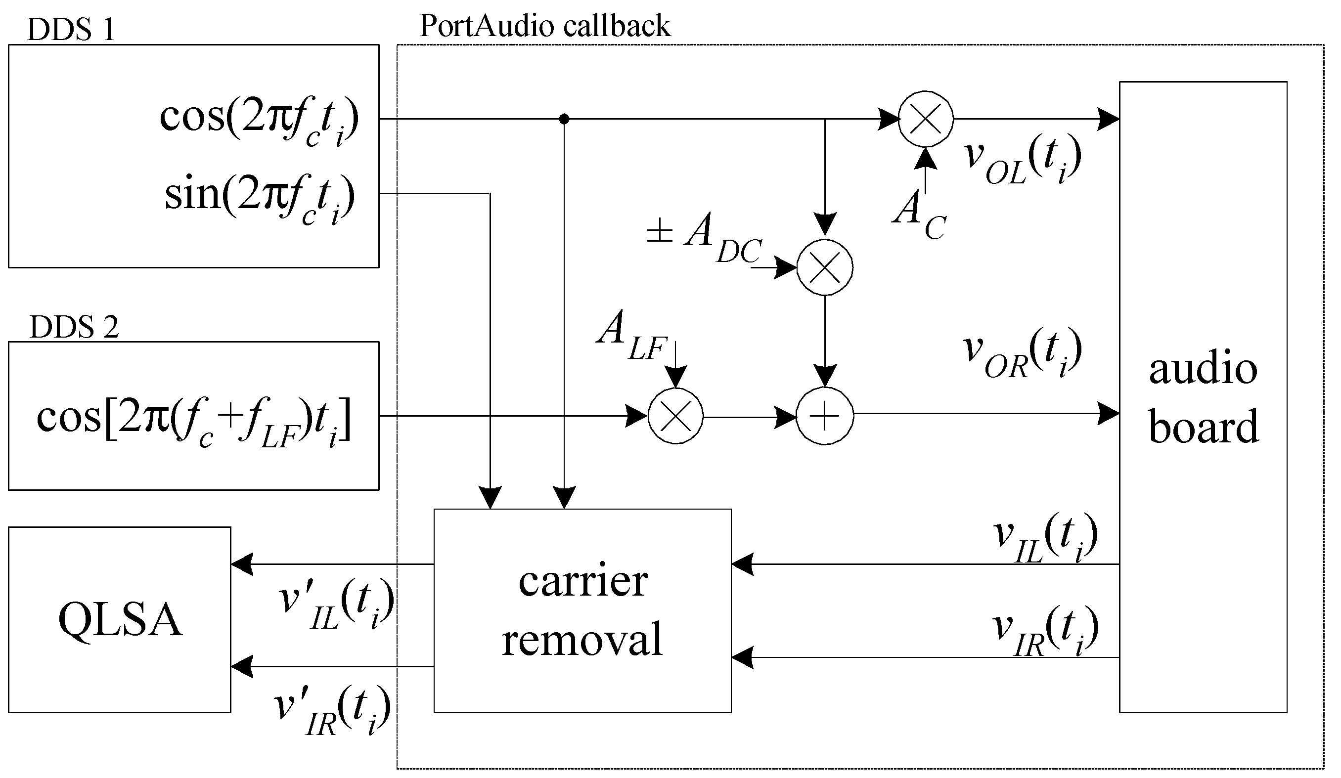
2.3. Digital Signal Elaboration Software

The fundamental operations that must be performed by the personal computer for the system in Figure 2 to operate correctly are the generation of the signals v O R and   v O L , the acquisition of the signals   v I L and v O R and the extraction of the modulus and the phase of each sinusiodal component in each channel so that the admittance can be estimated according to Equation (16). All software was developed in C, and it is freely available as it is based on public domain libraries. For controlling the sound board, we resorted to the public domain PortAudio [40] library. For signal generation, we developed a simple library for the software implementation of sinusoidal Numerically Controlled Oscillators (NCOs), while for the analysis of the acquired signals and the extraction of the admittance of the DUT we relied on the Narrow Band (NB) estimation extension of the QLSA public domain library [35,36].
Signal generation, acquisition, and elaboration all revolve around a PortAudio callback function for managing real time operation of the system. The callback is activated any time a new record of input data becomes available in the input buffer and a new record of output data has to be sent to the output buffer. Any time the callback is activated, NS samples are retrieved for each of the two input channels and NS samples are inserted into the output buffer for each of the two output channels. The number of samples NS is chosen as a power of 2 (typically ranging from 212 up 215) as this simplifies the interface to the QLSA library that can only accept records with a number of samples for each channel that is a power of 2. In order to reduce the computational load for the PC, signal generation is performed by resorting to a software implementation of the approach discussed in [41] that is the basis for many modern Direct Digital Synthesis integrated circuits. We used 30-bit phase accumulators that, with a standard sampling frequency fCK = 48 kHz for the audio board, resulted in a frequency resolution of 44.7 μHz. Values of sin(x) and cos(x) were obtained starting from a 216 locations look-up table using the 16 most significant bits of the phase accumulators for addressing the table, with the remaining 14 bits being used for linear interpolation between adjacent look-up table entries. Calculations were performed in floating point and samples were sent to PortAudio in the same format. Overall, the error in the values of sin(x) was maintained well below 1 LSB of a 24 bit DA converter with an output dynamic of ±1 V. Two independent signal sources were implemented (DDS 1 and DDS 2 in Figure 3). The cosinusoidal outputs from the two DDSs were used to generate the records of samples to be sent to the audio board output in order to create the   v O R and   v O L signals in Equations (1) and (2). The DDS used to generate the carrier (DDS 1) also outputs a quadrature signal that can be used in the “carrier removal” block in Figure 3. The role of the carrier removal block is best discussed in conjunction with the way in which QLSA is used to extract information on the impedance of the DUT from the   v I L and   v I R signals. It must be pointed out that resorting to QLSA for extracting impedance information from   v I L and   v I R is not mandatory: other numerical procedures can be implemented. However, besides the fact that QLSA, with its NB extension, is readily available, a few of its features greatly help in simplifying the measurement procedure, as we shall discuss in the next sections. As discussed in [35], QLSA is a library for simplifying the implementation of spectral analysis applications especially in the field of low frequency noise measurements. In this work, we are, however, interested in the NB extension that was mainly introduced to simplify the analysis of strongly peaked noise spectra as discussed in detail in [36]. For the correct operation of QLSA, records of the sampled signals need to be continuously fed to its internal engine. Samples relative to M input signals must be fed to QLSA in the form of an array of interleaved samples with a length exactly equal to M × NR, where NR is the record length that must be a power of 2 and must be selected upon initialization. In NB mode, QLSA allows the estimation of the power spectra of all input channels, together with the cross spectra among them, in a frequency interval from fmin to fmax, with fmin and fmax defined by the user, and with a frequency resolution ΔfNB given by:
Δ f N B = f m a x f m i n N R   ;   f m a x ,   f m i n < f C K 2  
More importantly, in NB mode, the Equivalent Noise Bandwidth (ENB) of the filter used for the estimation of the power spectrum across each frequency within the interval in Equation (18) can be set independently of the sampling frequency fCK and the record length NR. In particular, as discussed in detail in [36], QLSA can perform spectral estimation for several different ENBs at the same time with:
E N B i = 1 p i 1 + p i × f C K N R ;   0 < p i < 1
where pi is a set of values defined by the user before starting the measurements.
The ability to set estimation filters across each frequency with a very narrow ENB is a key requirement in the case of our application. When a sinusoidal signal is at the input of a spectrum analyzer, one obtains a non-zero output not only at the frequency of the input signal but also at other frequencies depending on the frequency response of the filter used for the estimation [42]. Typically, we obtain the maximum in the response at the frequency of the input signal, and we may want to employ filters with very narrow ENB to improve the signal-to-noise ratio. When more than one sinusoid is present at the input, the response corresponding to the different sinusoids superimposes and, in some cases, the presence of a sinusoid with a large amplitude may completely mask the presence of another sinusoid at a close frequency with a much smaller amplitude. This is indeed the case in the application we are interested in and, therefore, great care must be paid to selecting the most proper frequency response for the estimation filter. It is worth noting that the time required to complete a measurement is, roughly, inversely proportional to the ENB of the filter being employed, so one must always find a compromise between selectivity and measurement time. In this respect, the fact that QLSA allows the estimation of spectra using a number of different ENBs at the same time represents an important feature since one can stop the measurement as soon as the measurements corresponding to the ENB that allow sufficient selectivity become available. In order to better understand this aspect and to justify the need for the carrier removal block in Figure 3, we reported some spectra estimations obtained by feeding synthetic data to QLSA. The spectra reported in Figure 4 were obtained setting a standard sampling frequency of fCK = 48 kHz, a carrier frequency fC = 10 kHz; the frequency of the test signal   v V D (Figure 1) was set to fLF = 100 mHz and its amplitude was set to 10 mV. In this condition, and with a zero DC component, the power spectra evaluated by QLSA in NB mode in a frequency interval of 1 Hz across the carrier, with NR = 214 and for a few different NEBs, are reported in Figure 4a. Because of the modulation performed by M2 in Figure 1, we obtain two sinusoidal components at frequencies fCfLF and fC + fLF. As we had anticipated, we obtain a non-zero spectrum over a rather wide interval across the frequency of the sinusoids at the input of the system. This phenomenon is normally referred to as “spectral leakage”. If a sufficiently narrow NEB is used (for example 11 mHz or 2.9 mHz), we can assume that the maximum of the spectrum at fCfLF is not significantly modified by the presence of the sinusoid at fC + fLF with respect to the case in which only a sinusoid at fCfLF was present, and the same is true for the peak value at fC + fFL. On the other hand, if the NEB becomes larger (for instance 46 mHz as in Figure 4a), the effect of the spectral leakage is significant and the extraction of the amplitude of the sinusoids contributing to the overall spectrum becomes challenging because of the reciprocal influence among them. The situation becomes much more severe in the case in which a third sinusoid is present with a much larger amplitude. This is indeed quite a common occurrence in our application. Indeed, we typically would like to extract the impedance of the DUT using a small AC excitation in the presence of non-zero DC voltage across the DUT. In our system, a large DC component across the DUT translates into a large sinusoidal component at the carrier frequency. The resulting spectra as estimated by QLSA in the very same conditions as before, but with a 100 mV DC component across the DUT, are reported in Figure 4b. As it is apparent, the large leakage from the large sinusoidal component at fC completely masks the presence of the frequency components at fCfLF and fC + fLF for an NEB of 46 mHz and it is clear that we need to operate with NEBs much smaller than in the case of Figure 4a if we have to make the influence from the leakage of the sinusoid at fC negligible as far as the estimation of the components at fCfLF and fC + fLF are concerned. In principle, using QLSA and setting a proper value of pi in Equation (19) we can obtain an NEB as narrow as necessary, but this might result in extremely long measurement times. The problem is especially relevant for the lowest frequencies of interest, where measurement time is already intrinsically long. As an alternative, one could numerically subtract the components at fC in both   v I L and   v I R in Figure 3 before sending the data stream to QLSA. This clearly requires exact knowledge of the amplitude and phase of the sinusoidal signal to be subtracted, which can be obtained as part of the measurement configuration sequence: any time a new DC value is set across the DUT, the system is operated with no AC component so that proper coefficients can be adjusted in the carrier subtraction block in Figure 3.
When spectra (and cross spectra) with well-defined peaks at fCfLF and fC + fLF are obtained, we can extract the value of the impedance of the DUT according to the following procedure. The relationship between signals and DUT impedance summarized by Equation (16) can be represented by the signal chain reported in Figure 5. As long as the frequency response H is such that at frequency fC + fLF we have:
H ( f C + f L F ) = A R L F Y D L F e j ( φ R L F + φ D L F )
the relationship between   v IL 3 and   v IR 3 obtained from Figure 5 is the same as the one obtained in Equations (13) and (14). From the general properties of spectra and cross spectra, with reference to Figure 5, we have:
S R L ( f C + f L F ) = S L L ( f C + f L F ) H ( f C + f L F )
where SRL is the cross spectrum between the output and input signals and SLL is the power spectrum of the input signal in Figure 5. Since the values of SRL and SLL at fC + fLF are provided by QLSA, we can use Equation (21) to obtain an estimate of H and, from Equation (16) and the knowledge of the transfer function of the TIA in Figure 2, the desired estimate of the impedance of the DUT at fLF.
The very same information can be clearly obtained from the spectra and cross spectra evaluated at fC − fLF. In general, one can average the results obtained at the two frequencies in order to reduce the random error in the estimate.

3. Results and Discussion

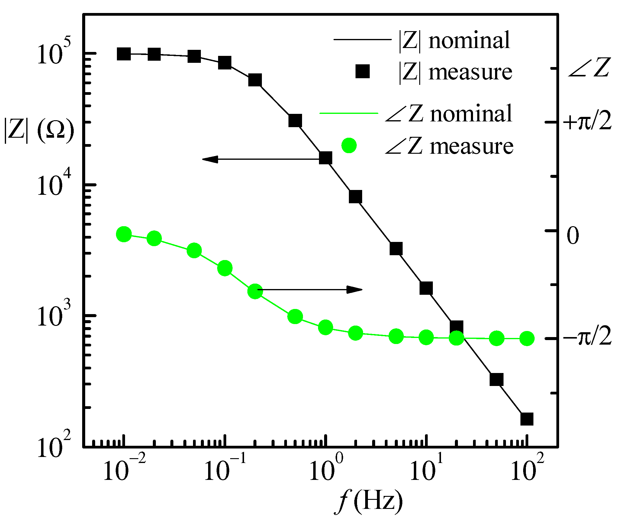
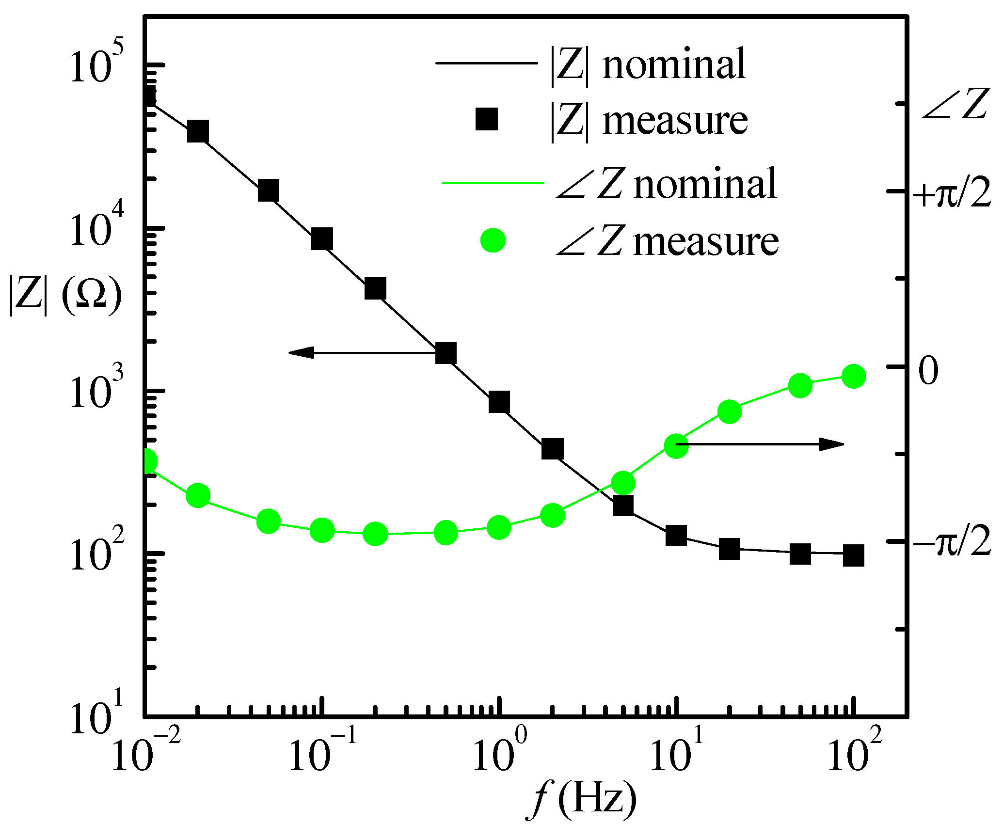
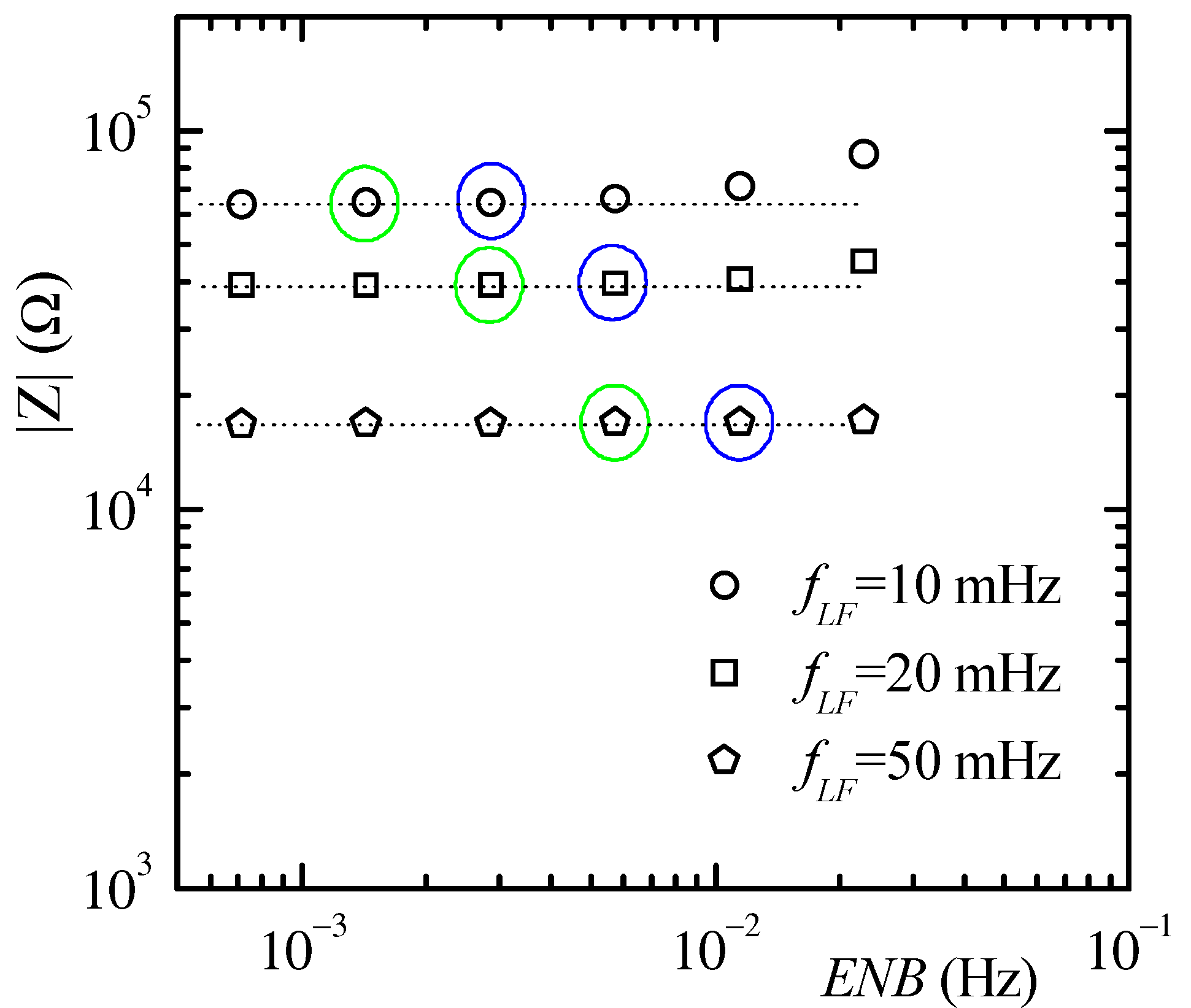
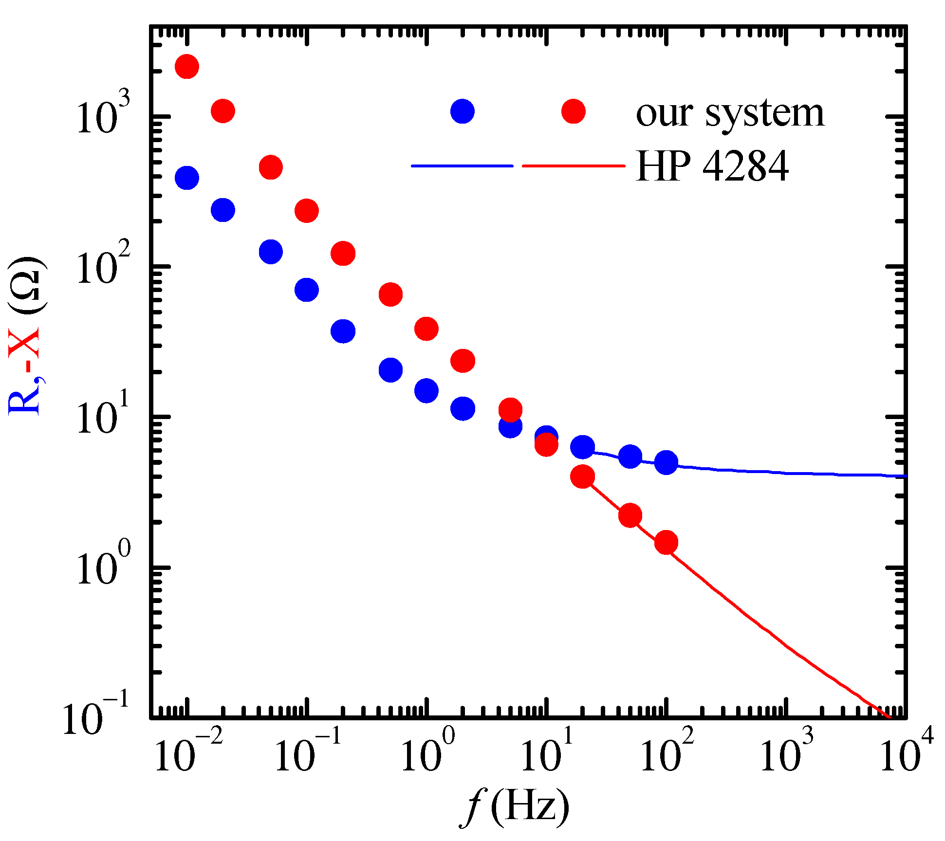
3.1. Preliminary System Testing

Measurements were performed with the system in Figure 2 using the “opt 1” configuration option, that is, with   v V D = v D U T . The USB audio interface Behringer UMC202HD was used as the audio board configured for 24 bit and 48 kHz sampling frequency. All measurements were performed with RR = 1 kΩ an CR = 680 nF.
As a first experiment, we performed measurements on the DUT in Figure 6a in the frequency range between 10 mHz and 100 Hz. In this experiment, the value of the DC bias voltage was set to 0 and the AC amplitude was set to 10 mV. It is worth noting that with this setting, at the lowest explored frequency (10 mHz), the amplitude of the AC voltage at the output of the TIA is about 100 μV. Since the input dynamic range of M3 in Figure 2 is ±1 V, we could have selected different values of RR and CR in order to obtain a larger |AR| and, hence, better coverage of the input dynamic range. The measurement condition we have selected, on the other hand, allows us to demonstrate that quite accurate results can be obtained also in such an unfavorable condition. QLSA was set to operate with a record length NR = 215 (32,768) and 11 geometrically decreasing ENBs were selected with:
E N B j = f C K 2 j N R ;   1 < j < 11
The largest ENB is therefore about 732 mHz, while the narrowest ENB is as low at 715 μHz. Different choices are possible, also on a per-measurement basis, and the cost of adding more ENB values is very small in terms of computational load. In principle, one should employ the narrowest ENB in any situation in order to improve the signal-to-noise ratio and reduce leakage effects. However, reducing the ENB results in increasing the measurement time, and therefore, one needs to find a compromise. Moreover, spectra and cross spectra typically need to be averaged a few times in order to reduce statistical errors, and this also contributes to the overall measurement time. When QLSA operates in NB mode, the wait time TW(M) after which spectra with M averages corresponding to a given ENB are available is given by:
T W ( M ) = α + ( M 1 )   β E B N   ;   α 1.165   ,   β 0.35
When a deterministic sinusoidal signal is present, as in the situations in Figure 4, only a small number of averages are usually required. To provide a better sense of the measurement time required in each case, the wait times for the first estimate (TW(1)) and the wait time after four averages (TW(4)) vs. the ENBs in Equation (22) are reported in Figure 7.
With reference to Figure 4, it can be estimated that in the presence of a negligible DC component, in order to avoid errors due to spectral leakage, we should employ an ENB that is at least 1/10 of the frequency separation between the peaks to be estimated (at fCfLF and fC + fLF), that is we must work with ENB < fLF/5. Let us now assume that we want to perform measurements at 10 mHz. According to the criterion above, we should refer to ENB10 = 1.43 mHz among the selected ENBs in Equation (22) to ensure negligible leakage errors. This choice, from Figure 7, would result in a measurement time, for obtaining four averages, of about 1500 s. While this may appear quite a long time, it is worth noticing that it corresponds to just 15 periods of the input signal. Moreover, as we shall discuss in the following, larger ENBs can usually be used without introducing large errors, thus considerably reducing the measurement time. As the test frequency increases, shorter and shorter measurement times are required, and this leads to the conclusion that the overall measurement time is essentially set by the lowest frequency of interest.
The results of the measurements on the first test DUT (Figure 6a) are reported in Figure 8 (symbols) and compared to the expected calculated values (continuous lines). As it is apparent, a quite good agreement is obtained with the DUT impedance values changing by a factor of about 1000 over the explored frequency range.
A second set of test measurements was performed on the test impedance in Figure 6b. The 200 μF capacitor was obtained as the parallel of 20 10 μF polyester capacitors. The amplitude for the AC signal was still 10 mV, but in this case, a DC bias of 500 mV was also present with the carrier removal block in Figure 3 active to reduce the leakage from the peak at the carrier frequency. As before, as can be noted in Figure 9, a quite good agreement is obtained between measured data (symbols) and expected values (continuous lines).
As we have mentioned above, the values of the impedance reported in Figure 8 and Figure 9 were extracted from the spectra estimated with the largest available ENB for which ENB < fLF/5. It must be noted, however, the QLSA performs the calculation of the spectra corresponding to all the different available ENBs in parallel. This means, for instance, that even if we focus on ENB10 for fLF = 10 mHz, as in the example discussed above, spectra corresponding ENB9, ENB8, and so on are being calculated as well and, because of Equation (23), estimates corresponding to lower index ENBs become available before the first estimate for a higher index ENB is available. This means that by observing the estimates obtained for lower index ENBs as they become available, if consistent data are obtained for increasing indexes, one can stop the measurement before the estimate for the targeted high index ENB is obtained, thus saving time. This is exemplified in Figure 10 where the estimate of the modulus of the impedance of the DUT in Figure 10 is reported for the three lowest frequencies vs. ENB. The symbols encircled in green represent the measurement points reported in Figure 9 and corresponding to ENB < fLF/5. If one had to build the sequence of symbols corresponding to one of the measurement frequencies in Figure 10 in real time during the measurement, the symbols at the right would become available first, followed by the symbol at their left and so on until enough time is elapsed for the estimation corresponding to the leftmost symbols to become available. In observing each sequence of symbols as they become available, it could have been assumed with great confidence that the symbols encircled in blue would have represented the correct value of |Z| even before the symbols encircled in green (the ones actually used in Figure 9) would have become available, thus saving measurement time. The ability to monitor the progress of the estimation over a number of different ENB settings at the same time is a peculiar feature that is available in QLSA and that, to the best of our knowledge, has no equivalent in other measurement approaches. Proper application software can therefore be developed, based on this unique feature, to optimize measurement time while ensuring the absence of errors due to spectral leakage.

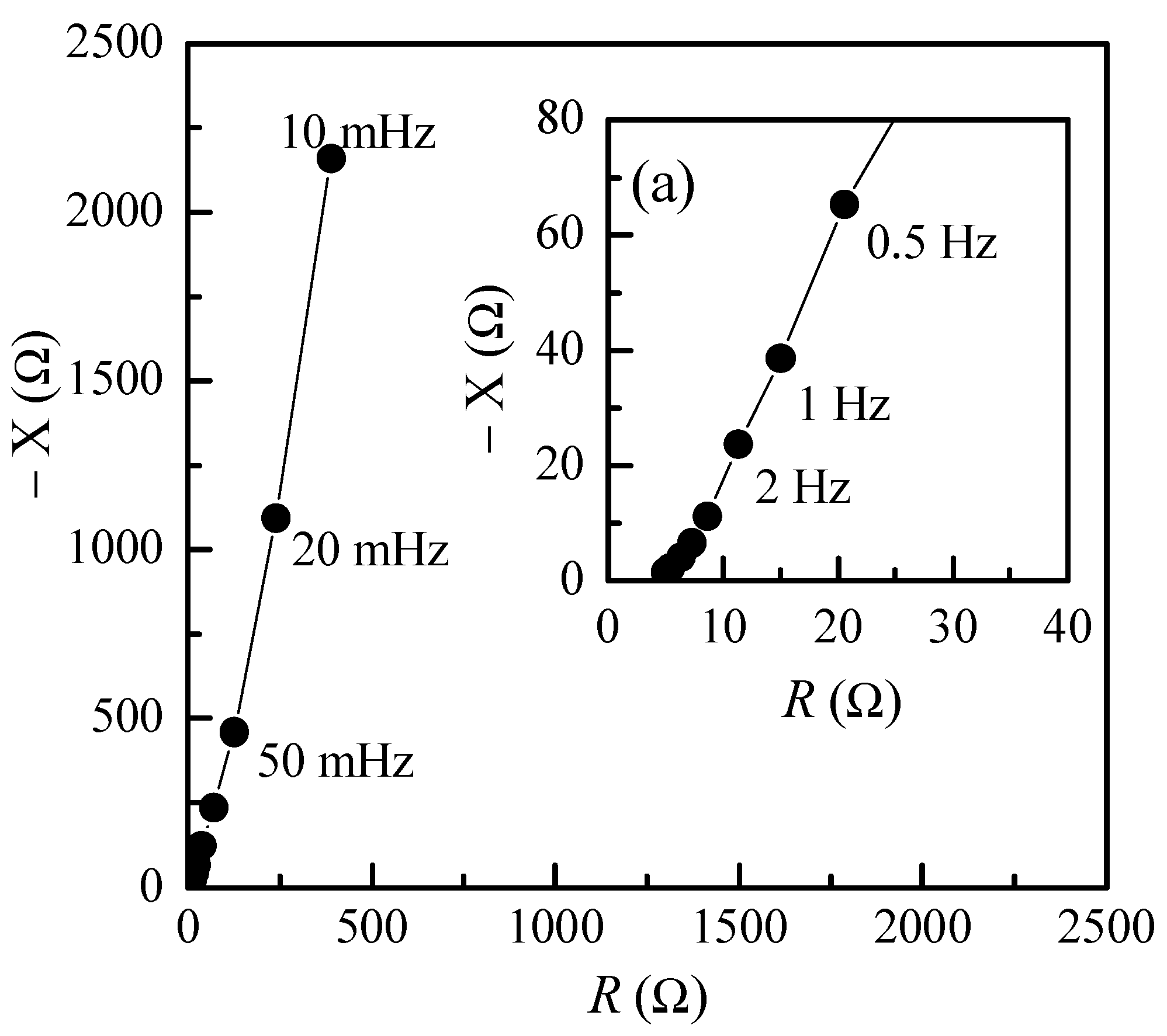
3.2. System Testing: An Example of Application

Following the preliminary tests, performed on well-known DUTs and intended to verify the soundness of the approach we propose, we performed the characterization of a prototype supercapacitor using symmetric electrodes based on polypyrrole (PPY). In common with other conjugated polymers, PPY has alternating single and double carbon-carbon bonds and the ability to undergo electrically driven reversible transition between its oxidized and reduced form, which has been exploited in actuators emulating artificial muscles [43], in electrochromic windows [44], and in a variety of applications going from electrochemical sensing [45,46] to energy storage and conversion [47,48,49,50,51,52]. Conducting electrodes to be used in electrochemical energy storage devices can be developed starting from commercially available insoluble PPY powder, as we attempt to do here, or by using PPY polymerized from its monomer and doped, or by combining PPY with a variety of other materials including nanostructured carbon and metal oxides, to yield nanocomposites with tailored electrical, and electrochemical properties [53,54,55]. Because of their electrochemical activity, electrodes based on PPY and its nanocomposites, when applied in a planar supercapacitor configuration, namely when impregnated with an electrolyte and separated from another electrode through an ion-permeable medium, confer to the device a faradaic character. Meaning that the energy storage mechanism in supercapacitors having PPY based electrodes is not only the electrically driven absorption-desorption of anions and cations at the electrodes, as is the case in electric double layer capacitors but is also the occurrence of fast redox transition at the surface of the PPY electrode, as it happens in the so-called pseudo-capacitor. The performance of each supercapacitor, which strictly depends on the composition, and on the structural, electrical, and electrochemical properties of its electrodes, can be evaluated using impedance spectroscopy, and low frequency measurements provide important information on the device characteristics. The DUT examined here is a flexible symmetric pseudo-capacitor developed using a substrate transparency sheet having a gold film evaporated in a vacuum on the top. The electrode material is obtained as a clear aqueous suspension by diluting in deionized water the doped polypyrrole (PPY) powder (purchased from Aldrich, Merck KGaA, Darmstadt, Germany) dispersed in Dodecylbenzenesulfonic acid (DBSA, 70% in isopropanol, Aldrich), at a ratio of 1:4 by weight. The PPy-DBSA dispersion is used as ink to fill rechargeable pens and is applied on the top of the gold-coated transparency. After few minutes of storage at about 60 °C to remove the residual solvent, a layer deposited from a mixture of 300 mg of lithium hexafluorophospate (LiPF6) and 3 mL of Nafion (D2029, purchased from Ion Power GmbH, Terminalstraße Mitte 18, München, Germany) in 10 mL of ethanol, is applied on the top of the PYR-DBSA electrode. After this latter layer is left to dry slowly, an ion-permeable Nafion membrane impregnated with the lithium salt, forms on the PYR-DBSA electrode. At this stage, the transparency sheet is cut into a couple of pieces that are faced to each other and stored at about 60 °C for a few tens of seconds, in order to achieve adherence of the two pieces. The developed device is a symmetric system the schematic view of which is shown in Figure 11.
Full characterization of the device in Figure 11 is under development. Here we are interested in the ability of the system we designed to provide data on the impedance of the device at a very low frequency. The real part of the impedance (R) and the opposite of the imaginary part (−X) of the DUT as obtained using the approach we propose are reported in Figure 12 (symbols). The explored frequency range was from 10 mHz up to 100 Hz. A standard LCR meter HP4284 was also used to measure the impedance of the DUT. The HP4284 minimum test frequency is 20 Hz and the values of R and −X obtained for the device in Figure 11 are also reported in Figure 12 (continuous lines). As it can be noticed, we obtain essentially the same result with the standard LCR meter and with the system in Figure 2 in the frequency range in which the explored frequency range for the two instruments overlap (from 20 to 100 Hz). This fact is a further indication of the soundness of the approach we propose. In the particular case of the results reported in Figure 12, it is interesting to notice that at frequencies below 500 mHz, the reactance (X) of the device shows the same frequency dependence that would be expected from an ideal capacitor (|X| ∝ 1/f). While this fact, because of the complexity of systems such as the one tested in this work, does not allow, in itself, to draw a definite conclusion on the nature of the conduction mechanisms occurring in the device, it certainly demonstrates that exploring very low frequencies, as can be done with the system we propose, can provide information that would be otherwise hidden because of the limitation of standard instrumentation.
When investigating the electrical properties of devices and materials by means of EIS, Nyquist plots may result in a useful representation in the process of the extraction of an equivalent circuit [56]. If we use the data in Figure 12 to create the Nyquist plot, we obtain Figure 13. It can be noticed that the plot exhibits an almost vertical line that approaches 90° in the low frequency region, which corresponds to an ideal capacitor and fast ion diffusion in electrode materials [57]. The results obtained are in agreement with what has been reported in the literature about characterizations performed on similar structures [55].

4. Conclusions

In this paper, a platform for low frequency impedance measurements has been designed, implemented, and tested. In the proposed approach, we exploit a personal computer and a sound board as a powerful system for digital signal generation and analysis that, with the help of a low complexity and low-cost external hardware, allows to perform low frequency impedance measurements for various applications. For the implementation of the core system, we resort to public domain software, so that, together with the simple hardware, the system can be easily reproduced by researchers interested in EIS and tailored for targeting specific applications with minimal effort. To demonstrate the effectiveness of the proposed measurement system, we performed measurements both on conventional electronic components as DUTs and on a prototype of polypyrrole-based supercapacitor structure. The results have been compared with measurements performed by means of a standard LCR meter in the frequency range in which the explored frequency ranges for the two instruments overlap. The results showed that the instrument is highly versatile and accurate and can be used in all those applications that require low frequency impedance measurements, ranging from bioengineering to energy applications.

Author Contributions

Conceptualization, G.S. and A.A.; methodology, C.C. and G.S.; software, C.C.; validation, C.C., A.A., and G.S.; formal analysis, E.C. and G.G.; investigation, G.S.; data curation, C.C.; writing—original draft preparation, G.S. and C.C.; writing—review and editing, E.C. and G.G.; visualization, A.A.; supervision, C.C. and G.S. All authors have read and agreed to the published version of the manuscript.

Funding

This research received no external funding.

Data Availability Statement

Data are contained within the article. The data presented in this study can be requested from the authors.

Conflicts of Interest

The authors declare no conflict of interest.

References

  1. Młyńczak, M.; Rosoł, M.; Spinelli, A.; Dziki, A.; Wlaźlak, E.; Surkont, G.; Krzycka, M.; Pająk, P.; Dziki, Ł.; Mik, M.; et al. Obstetric Anal Sphincter Injury Detection Using Impedance Spectroscopy with the ONIRY Probe. Appl. Sci. 2021, 11, 637. [Google Scholar] [CrossRef]
  2. Jin, K.; Zhao, P.; Fang, W.; Zhai, Y.; Hu, S.; Ma, H.; Li, J. An Impedance Sensor in Detection of Immunoglobulin G with Interdigitated Electrodes on Flexible Substrate. Appl. Sci. 2020, 10, 4012. [Google Scholar] [CrossRef]
  3. Scandurra, G.; Cardillo, E.; Giusi, G.; Ciofi, C.; Alonso, E.; Giannetti, R. Portable Knee Health Monitoring System by Impedance Spectroscopy Based on Audio-Board. Electronics 2021, 10, 460. [Google Scholar] [CrossRef]
  4. Arpaia, P.; Cesaro, U.; Frosolone, M.; Moccaldi, N.; Taglialatela, M. A micro-bioimpedance meter for monitoring insulin bioavailability in personalized diabetes therapy. Sci. Rep. 2020, 10, 13656. [Google Scholar] [CrossRef]
  5. Coates, J.; Chipperfield, A.; Clough, G. Wearable Multimodal Skin Sensing for the Diabetic Foot. Electronics 2016, 5, 45. [Google Scholar] [CrossRef] [Green Version]
  6. Zink, M.D.; König, F.; Weyer, S.; Willmes, K.; Leonhardt, S.; Marx, N.; Napp, A. Segmental bioelectrical impedance spec-troscopy to monitor fluid status in heart failure. Sci. Rep. 2020, 10, 3577. [Google Scholar] [CrossRef]
  7. Jotta, B.; Coutinho, A.B.B.; Pino, A.V.; Souza, M.N. Lactate threshold by muscle electrical impedance in professional rowers. Rev. Sci. Instrum. 2017, 88, 045105. [Google Scholar] [CrossRef]
  8. Morais, A.P.; Pino, A.V.; Souza, M.N. Detection of questionable occlusal carious lesions using an electrical bioimpedance method with fractional electrical model. Rev. Sci. Instrum. 2016, 87, 084305. [Google Scholar] [CrossRef]
  9. Vázquez-Nambo, M.; Gutiérrez-Gnecchi, J.-A.; Reyes-Archundia, E.; Yang, W.; Rodriguez-Frias, M.-A.; Olivares-Rojas, J.-C.; Lorias-Espinoza, D. Experimental Study of Electrical Properties of Pharmaceutical Materials by Electrical Impedance Spectroscopy. Appl. Sci. 2020, 10, 6576. [Google Scholar] [CrossRef]
  10. Maalouf, R.; Fournier-Wirth, C.; Coste, J.; Chebib, H.; Saïkali, Y.; Vittori, O.; Errachid, A.; Cloarec, J.-P.; Martelet, C.; Jaffrezic-Renault, N. Label-Free Detection of Bacteria by Electrochemical Impedance Spectroscopy: Comparison to Surface Plasmon Resonance. Anal. Chem. 2007, 79, 4879–4886. [Google Scholar] [CrossRef]
  11. Ruan, C.; Yang, L.; Li, Y. Immunobiosensor Chips for Detection ofEscherichiacoliO157:H7 Using Electrochemical Impedance Spectroscopy. Anal. Chem. 2002, 74, 4814–4820. [Google Scholar] [CrossRef]
  12. Nandakumar, V.; La Belle, J.T.; Reed, J.; Shah, M.; Cochran, D.; Joshi, L.; Alford, T.L. A methodology for rapid detection of Sal-monella typhimurium using label-free electrochemical impedance spectroscopy. Biosens. Bioelectron. 2008, 24, 1039–1042. [Google Scholar] [CrossRef]
  13. Naranjo-Hernández, D.; Reina-Tosina, J.; Min, M. Fundamentals, Recent Advances, and Future Challenges in Bioimpedance Devices for Healthcare Applications. J. Sens. 2019, 2019, 1–42. [Google Scholar] [CrossRef] [Green Version]
  14. Bhargavan, B.; Kanmogne, G.D. Differential Mechanisms of Inflammation and Endothelial Dysfunction by HIV-1 Subtype-B and Recombinant CRF02-AG Tat Proteins on Human Brain Microvascular Endothelial Cells: Implications for Viral Neuro-pathogenesis. Mol. Neurobiol. 2018, 55, 1352–1363. [Google Scholar] [CrossRef] [PubMed]
  15. Gabriel, S.; Lau, R.W.; Gabriel, C. The dielectric properties of biological tissues: II. Measurements in the frequency range 10 Hz to 20 GHz. Phys. Med. Biol. 1996, 41, 2251–2269. [Google Scholar] [CrossRef] [Green Version]
  16. Tang, J.; Lu, M.; Yin, W. Cellular structure analysis based on magnetic induction finite element method simulations and measurements. bioRxiv 2018. [Google Scholar] [CrossRef]
  17. Kyle, U.G.; Bosaeus, I.; De Lorenzo, A.D.; Deurenberg, P.; Elia, M.; Gómez, J.M.; Heitmann, B.L.; Kent-Smith, L.; Melchior, J.C.; Pirlich, M.; et al. Bioelectrical impedance analysis—Part I: Review of principles and methods. Clin. Nutr. 2004, 23, 1226–1243. [Google Scholar] [CrossRef] [PubMed]
  18. Fu, B.; Freeborn, T.J. Residual impedance effect on emulated bioimpedance measurements using Keysight E4990A precision impedance analyser. Measurement 2019, 134, 468–479. [Google Scholar] [CrossRef]
  19. Pérez, P.; Huertas, G.; Maldonado-Jacobi, A.; Martín, M.; Serrano, J.A.; Olmo, A.; Daza, P.; Yúfera, A. Sensing Cell-Culture Assays with Low-Cost Circuitry. Sci. Rep. 2018, 8, 1–11. [Google Scholar] [CrossRef] [PubMed]
  20. Huerta-Nuñez, L.F.E.; Gutierrez-Iglesias, G.; Martínez-Cuazitl, A.; Mata-Miranda, M.M.; Alvarez-Jiménez, V.D.; Sánchez-Monroy, V.; Golberg, A.; González-Díaz, C.A. A biosensor capable of identifying low quantities of breast cancer cells by electrical impedance spectroscopy. Sci. Rep. 2019, 9, 1–12. [Google Scholar] [CrossRef] [Green Version]
  21. Lukaski, H.C.; Moore, M. Bioelectrical Impedance Assessment of Wound Healing. J. Diabetes Sci. Technol. 2012, 6, 209–212. [Google Scholar] [CrossRef] [Green Version]
  22. García, E.; Pérez, P.; Olmo, A.; Díaz, R.; Huertas, G.; Yúfera, A. Data-Analytics Modeling of Electrical Impedance Measurements for Cell Culture Monitoring. Sensors 2019, 19, 4639. [Google Scholar] [CrossRef] [PubMed] [Green Version]
  23. Xu, Y.; Li, C.; Mei, W.; Guo, M.; Yang, Y. Equivalent circuit models for a biomembrane impedance sensor and analysis of electrochemical impedance spectra based on support vector regression Medical, Biological Engineering and Computing. Med. Biol. Eng. Comput. 2019, 57, 1515–1524. [Google Scholar] [CrossRef] [Green Version]
  24. Vizvari, Z.; Gyorfi, N.; Odry, A.; Sari, Z.; Klincsik, M.; Gergics, M.; Kovacs, L.; Kovacs, A.; Pal, J.; Karadi, Z.; et al. Physical Validation of a Residual Impedance Rejection Method during Ultra-Low Frequency Bio-Impedance Spectral Measurements. Sensors 2020, 20, 4686. [Google Scholar] [CrossRef]
  25. Karden, E.; Buller, S.; De Doncker, R.W. A frequency-domain approach to dynamical modeling of electrochemical power sources. Electrochim. Acta 2002, 47, 2347–2356. [Google Scholar] [CrossRef]
  26. Anjum, N.; Joyal, N.; Iroegbu, J.; Li, D.; Shen, C. Humidity-modulated properties of hydrogel polymer electrolytes for flexible supercapacitors. J. Power Sources 2021, 499, 229962. [Google Scholar] [CrossRef]
  27. Kötz, R.; Hahn, M.; Gallay, R. Temperature behavior and impedance fundamentals of supercapacitors. J. Power Sources 2006, 154, 550–555. [Google Scholar] [CrossRef]
  28. Ge, Y.; Xie, X.; Roscher, J.; Holze, R.; Qu, Q. How to measure and report the capacity of electrochemical double layers, supercapacitors, and their electrode materials. J. Solid State Electrochem. 2020, 24, 3215–3230. [Google Scholar] [CrossRef]
  29. Scott, J.; Hasan, R. New Results for Battery Impedance at Very Low Frequencies. IEEE Access 2019, 7, 106925–106930. [Google Scholar] [CrossRef]
  30. Solartron: Frequency Response Analyzer 1255. Available online: https://www.ameteksi.com/-/media/ameteksi/download_links/documentations/1255b/model-1255b.pdf?revision=4412c40c-8960-4a99-8d95-7b9d29604323 (accessed on 9 July 2021).
  31. Novocontrol: BETA Series Analyzers. Available online: https://www.novocontrol.de/php/ana_alpha_n.php (accessed on 9 July 2021).
  32. Zahner: Electrochemical Workstation IM6, User Brochure. Available online: http://zahner.de/pdf/b_im6ex.pdf (accessed on 9 July 2021).
  33. CorrTest, CS350 Electrochemical Workstation. Available online: https://www.corrtest.com.cn/producten/dhxgcz/t1/2016/0601/379.html (accessed on 9 July 2021).
  34. Hioki:LCR Meter IM3533. Available online: https://www.hioki.com/global/products/lcr-meters/10-mhz/id_6065 (accessed on 9 July 2021).
  35. Ciofi, C.; Scandurra, G.; Giusi, G. QLSA: A software library for spectral estimation in low-frequency noise measurementap-plications. Fluct. Noise Lett. 2019, 18, 1940004. [Google Scholar] [CrossRef]
  36. Scandurra, G.; Giusi, G.; Ciofi, C. Accurate QTF Sensing Approach by Means of Narrow Band Spectral Estimation. J. Sens. 2020, 2020, 1–10. [Google Scholar] [CrossRef]
  37. AD 835 Datasheet. AD835 (Rev. E). Available online: https://www.analog.com/media/en/technical-documentation/data-sheets/AD835.pdf (accessed on 19 July 2021).
  38. LTC 1063 Datasheet. LTC1063-DC Accurate, Clock-Tunable 5th Order Butterworth Lowpass Filter. Available online: https://www.analog.com/media/en/technical-documentation/data-sheets/1063fa.pdf (accessed on 19 July 2012).
  39. USB Audio Board Behringer U-PHORIA UMC202HD. Available online: https://www.behringer.com/behringer/product?modelCode=P0BJZ (accessed on 19 July 2021).
  40. PortAudio Libraries. Available online: www.portaudio.com (accessed on 19 July 2021).
  41. Tierney, J.; Rader, C.; Gold, B. A digital frequency synthesizer. IEEE Trans. Audio Electroacoust. 1971, 19, 48–57. [Google Scholar] [CrossRef]
  42. Jwo, D.-J.; Chang, W.-Y.; Wu, I.-H. Windowing Techniques, the Welch Method for Improvement of Power Spectrum Estimation. Comput. Mater. Contin. 2021, 67, 3983–4003. [Google Scholar] [CrossRef]
  43. Mirfakhrai, T.; Madden, J.D.W.; Baughman, R.H. Polymer artificial muscles. Mater. Today 2007, 10, 30–38. [Google Scholar] [CrossRef]
  44. Wang, H.F.; Barrett, M.; Duane, B.; Gu, J.; Zenhausern, F. Materials and processing of polymer-based electrochromic devices. Mater. Sci. Eng. B 2017, 228, 167–174. [Google Scholar] [CrossRef]
  45. Terán-Alcocer, Á.; Bravo-Plascencia, F.; Cevallos-Morillo, C.; Palma-Cando, A. Electrochemical Sensors Based on Conducting Polymers for the Aqueous Detection of Biologically Relevant Molecules. Nanomaterials 2021, 11, 252. [Google Scholar] [CrossRef]
  46. Lakard, B. Electrochemical Biosensors Based on Conducting Polymers: A Review. Appl. Sci. 2020, 10, 6614. [Google Scholar] [CrossRef]
  47. Hong, X.; Liu, Y.; Li, Y.; Wang, X.; Fu, J.; Wang, X. Application Progress of Polyaniline, Polypyrrole and Polythiophene in Lithium-Sulfur Batteries. Polymers 2020, 12, 331. [Google Scholar] [CrossRef] [Green Version]
  48. Gul, H.; Shah, A.-u.-H.A.; Bilal, S. Fabrication of Eco-Friendly Solid-State Symmetric Ultracapacitor Device Based on Co-Doped PANI/GO Composite. Polymers 2019, 11, 1315. [Google Scholar] [CrossRef] [Green Version]
  49. Kim, O.; Kwon, J.; Kim, S.; Xu, B.; Seo, K.; Park, C.; Do, W.; Bae, J.; Kang, S. Effect of PVP-Capped ZnO Nanoparticles with Enhanced Charge Transport on the Performance of P3HT/PCBM Polymer Solar Cells. Polymers 2019, 11, 1818. [Google Scholar] [CrossRef] [Green Version]
  50. Song, J.; Ma, G.; Qin, F.; Hu, L.; Luo, B.; Liu, T.; Yin, X.; Su, Z.; Zeng, Z.; Jiang, Y.; et al. High-Conductivity, Flexible and Transparent PEDOT:PSS Electrodes for High Performance Semi-Transparent Supercapacitors. Polymers 2020, 12, 450. [Google Scholar] [CrossRef] [PubMed] [Green Version]
  51. Asnawi, A.S.F.M.; Aziz, S.B.; Nofal, M.M.; Hamsan, M.H.; Brza, M.A.; Yusof, Y.M.; Abdilwahid, R.T.; Muzakir, S.K.; Kadir, M.F.Z. Glycerolized Li+ Ion Conducting Chitosan-Based Polymer Electrolyte for Energy Storage EDLC Device Applications with Relatively High Energy Density. Polymers 2020, 12, 1433. [Google Scholar] [CrossRef] [PubMed]
  52. Xia, C.; Hong, W.T.; Kim, Y.E.; Choe, W.-S.; Kim, D.-H.; Kim, J.K. Metal-Organic Decomposition-Mediated Nanoparticulate Vanadium Oxide Hole Transporting Buffer Layer for Polymer Bulk-Heterojunction Solar Cells. Polymers 2020, 12, 1791. [Google Scholar] [CrossRef] [PubMed]
  53. Huang, Y.; Li, H.; Wang, Z.; Zhu, M.; Pei, Z.; Xue, Q.; Zhi, C. Nanostructured Polypyrrole as a flexible electrode material of supercapacitor. Nano Energy 2016, 22, 422–438. [Google Scholar] [CrossRef]
  54. Khuyen, N.Q.; Kiefer, R.; Zondaka, Z.; Anbarjafari, G.; Peikolainen, A.-L.; Otero, T.F.; Tamm, T. Multifunctionality of Polypyrrole Polyethyleneoxide Composites: Concurrent Sensing, Actuation and Energy Storage. Polymers 2020, 12, 2060. [Google Scholar] [CrossRef] [PubMed]
  55. Kulandaivalu, S.; Azahari, M.N.M.; Azman, N.H.N.; Sulaiman, Y. Ultrahigh specific energy of layer by layer polypyrrole/graphene oxide/multi-walled carbon nanotube| polypyrrole/manganese oxide composite for supercapacitor. J. Energy Storage 2020, 28, 101219. [Google Scholar] [CrossRef]
  56. Huang, J.; Li, Z.; Liaw, B.Y.; Zhang, J. Graphical analysis of electrochemical impedance spectroscopy data in Bode and Nyquist representations. J. Power Sources 2016, 309, 82–98. [Google Scholar] [CrossRef]
  57. Khoh, W.-H.; Hong, J.-D. Layer-by-layer self-assembly of ultrathin multilayer films composed of magnetite/reduced graphene oxide bilayers for supercapacitor application. Colloids Surf. A 2013, 436, 104–112. [Google Scholar] [CrossRef]
Figure 1. Block diagram of the proposed approach.
Applsci 11 08234 g001
Figure 2. Complete schematic for the implementation of the proposed approach. Depending on applications, different Front Ends can be used.
Applsci 11 08234 g002
Figure 3. Simplified diagram illustrating the interaction among the different software routines for signal generation, acquisition, and elaboration.
Applsci 11 08234 g003
Figure 4. Spectra estimated by QLSA in NB mode when synthetic data are used for creating the signal VOL in Equation (2) with different settings for ENB. In (a) the DC level of the test signal across the DUT is set to 0, while in (b) we set a DC level of 100 mV across the DUT.
Applsci 11 08234 g004
Figure 5. Signal chain equivalent of the relationship between signals vIL3 and vIR3 as obtained in Equation (16).
Applsci 11 08234 g005
Figure 6. Impedances used for testing the proposed approach. Capacitor CPa in (a) is a 10 μF, 100 V polyester capacitor; capacitor CPb in (b) is obtained as the parallel of 20 10 μF, 100 V polyester capacitors.
Applsci 11 08234 g006
Figure 7. Measurement time for obtaining the first spectra estimation (TW(1)) and for reaching four averages (TW(4)) when using QLSA in NB mode vs. the selected ENB.
Applsci 11 08234 g007
Figure 8. Result of test measurements on the impedance in Figure 6a. DC bias across the DUT was set to 0 and the AC amplitude of the test voltage was 10 mV at all frequencies. Quite good agreement is obtained between measurements (symbols) and the expected values (solid lines).
Applsci 11 08234 g008
Figure 9. Result of test measurements on the impedance in Figure 6b. DC bias across the DUT was set to 500 mV and the AC amplitude of the test voltage was 10 mV at all frequencies. Quite good agreement is obtained between measurements (symbols) and the expected values (solid lines).
Applsci 11 08234 g009
Figure 10. Results of the estimation of the modulus of the impedance of the DUT in Figure 6b as a function of the ENB for the three lowest explored frequencies. It is apparent that if the ENB increases error is introduced because of spectral leakage. The data points used in Figure 9 are encircled in green. It is however apparent that data encircled in blue could have been used without significant error and reduced measurement time.
Applsci 11 08234 g010
Figure 11. Schematic view of the supercapacitor structure subjected to low frequency impedance measurements. The substrate (SUB) is cut out from a copier grade transparency sheet on top of which a gold layer (GOLD) was thermally evaporated. Electrodes are obtained from polypyrrole powder dispersed in Dodecylbenzenesulfonic acid (PPY-DBSA) and are separated by a mixture of Nafion and lithium hexafluorophospate (Nafion-LiPF6).
Applsci 11 08234 g011
Figure 12. Real (R) and imaginary (X) part of the impedance of the device in Figure 11 as measured by the system proposed in this paper (symbols, from 10 mHz to 100 Hz) and as measured using an HP 4284 LCR meter (solid line, above 20 Hz).
Applsci 11 08234 g012
Figure 13. Nyquist plot from the low frequency impedance data in Figure 12. Due to the large dynamic of the data on a linear scale, a magnified view of the data at higher frequencies is reported in the inset (a).
Applsci 11 08234 g013
Publisher’s Note: MDPI stays neutral with regard to jurisdictional claims in published maps and institutional affiliations.

