
Open Localization in 3D Package with TSV Daisy Chain Using Magnetic Field Imaging and High-Resolution Three-Dimensional X-ray Microscopy


Abstract
:1. Introduction
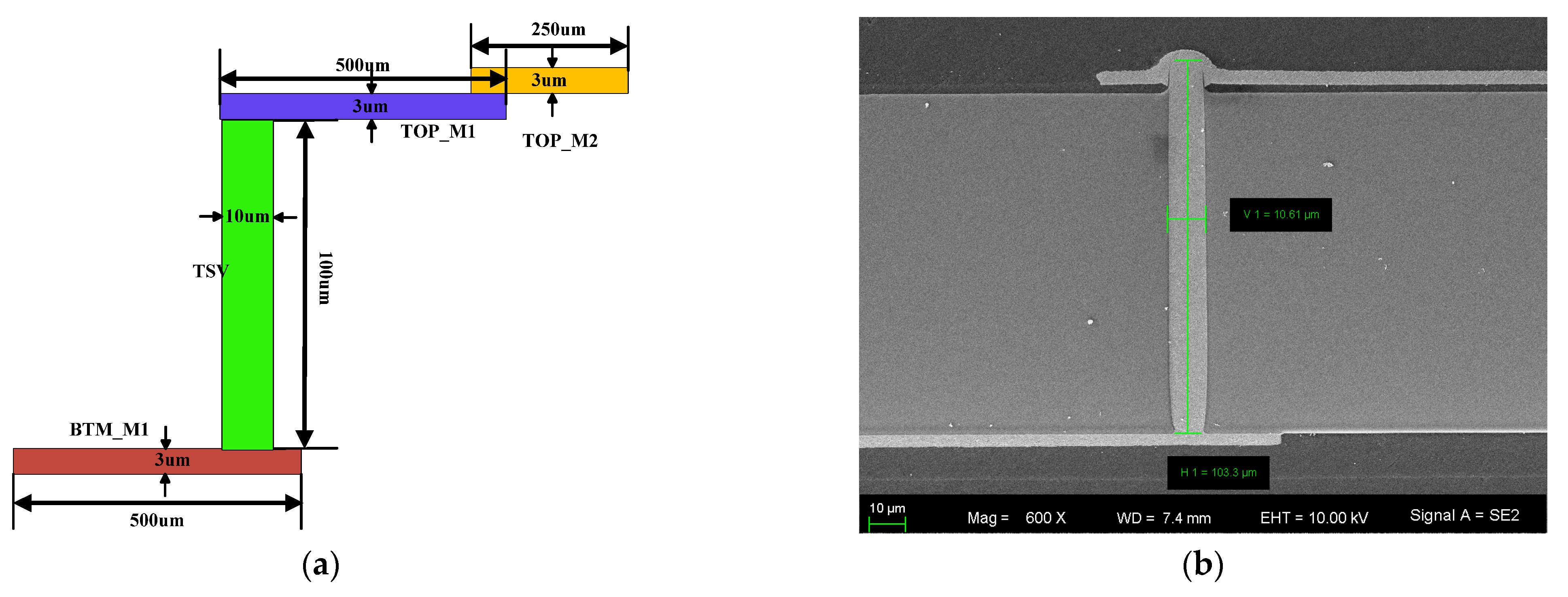
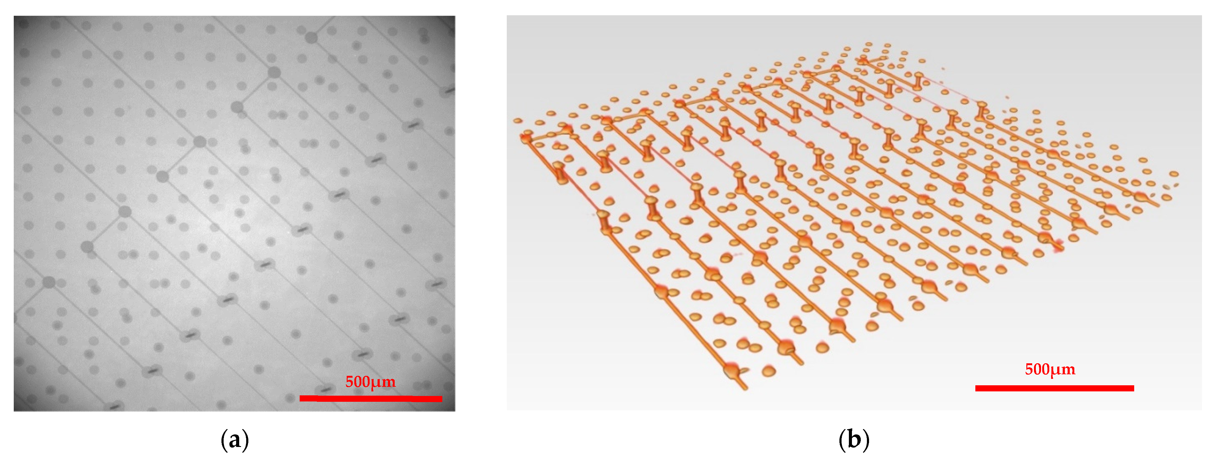
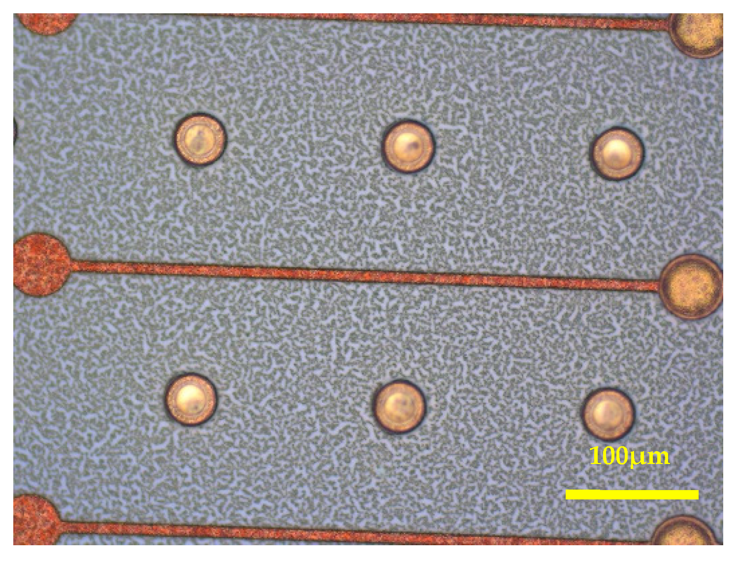
2. Test Sample
3. Defect Localization
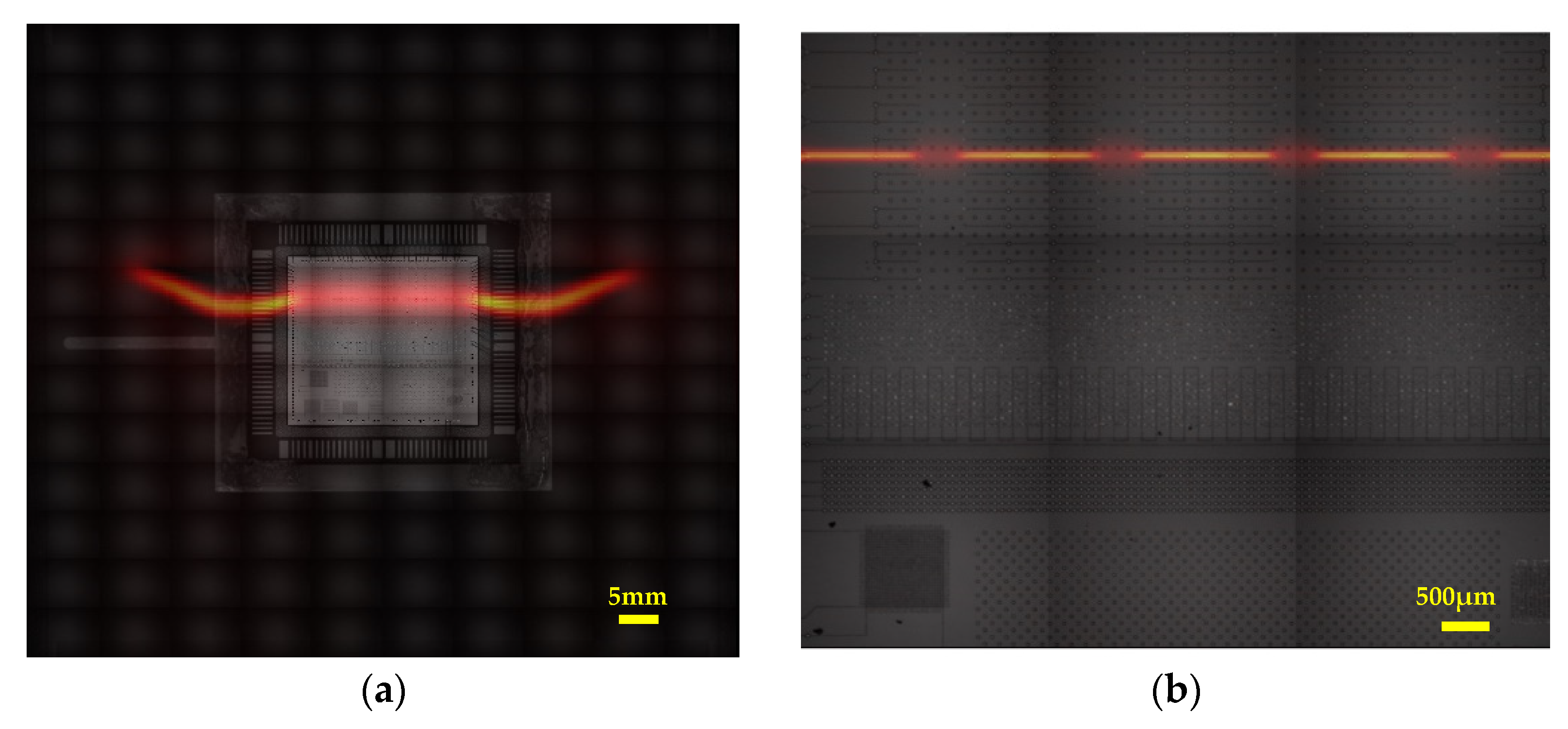
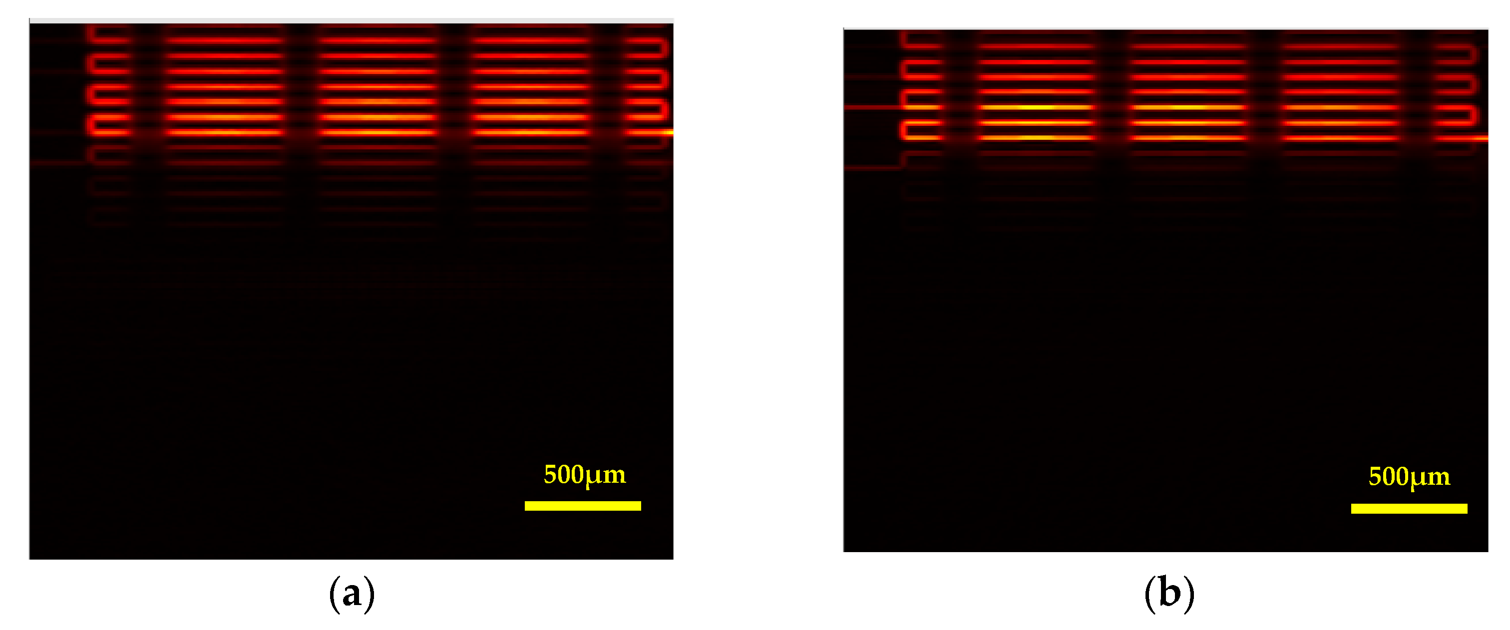
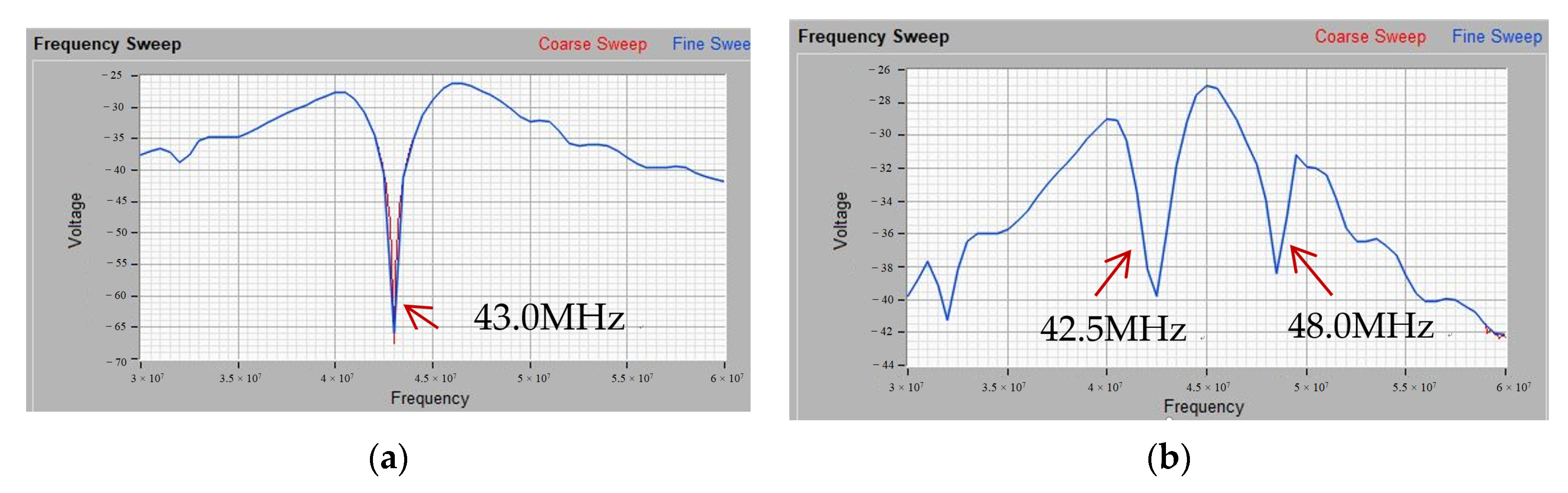
3.1. Magnetic Field Imaging
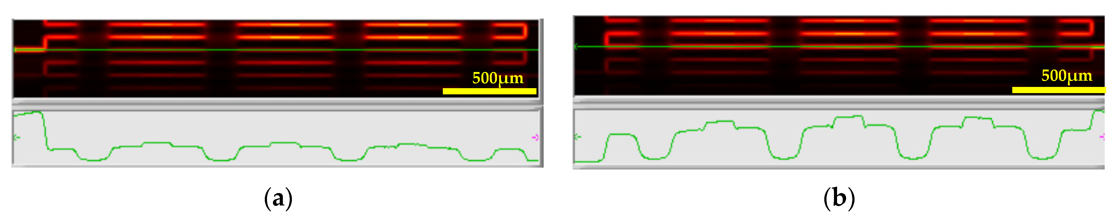
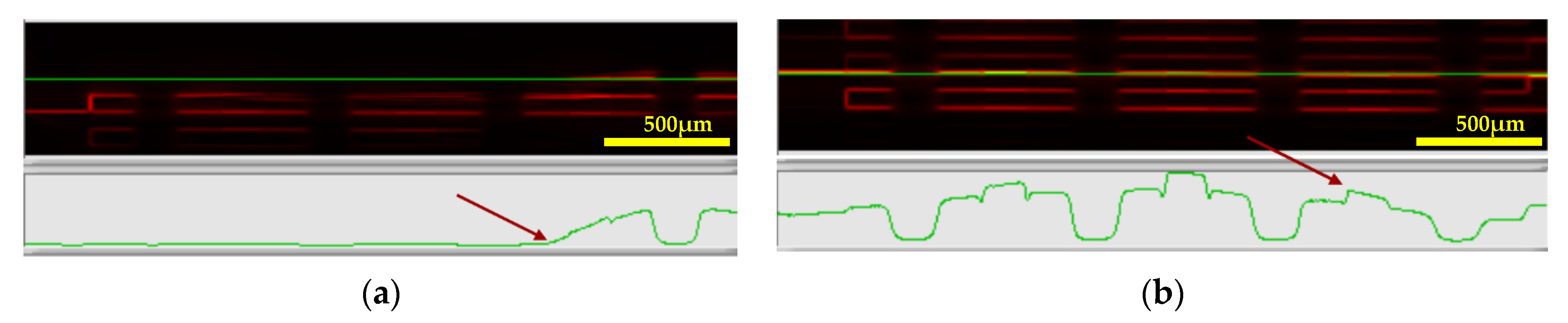
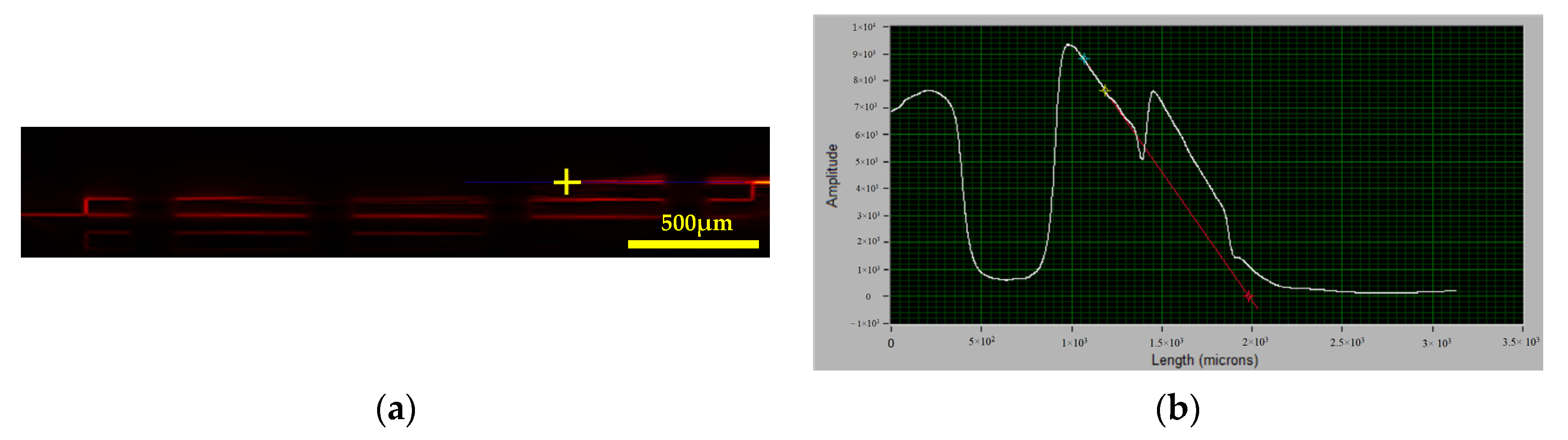
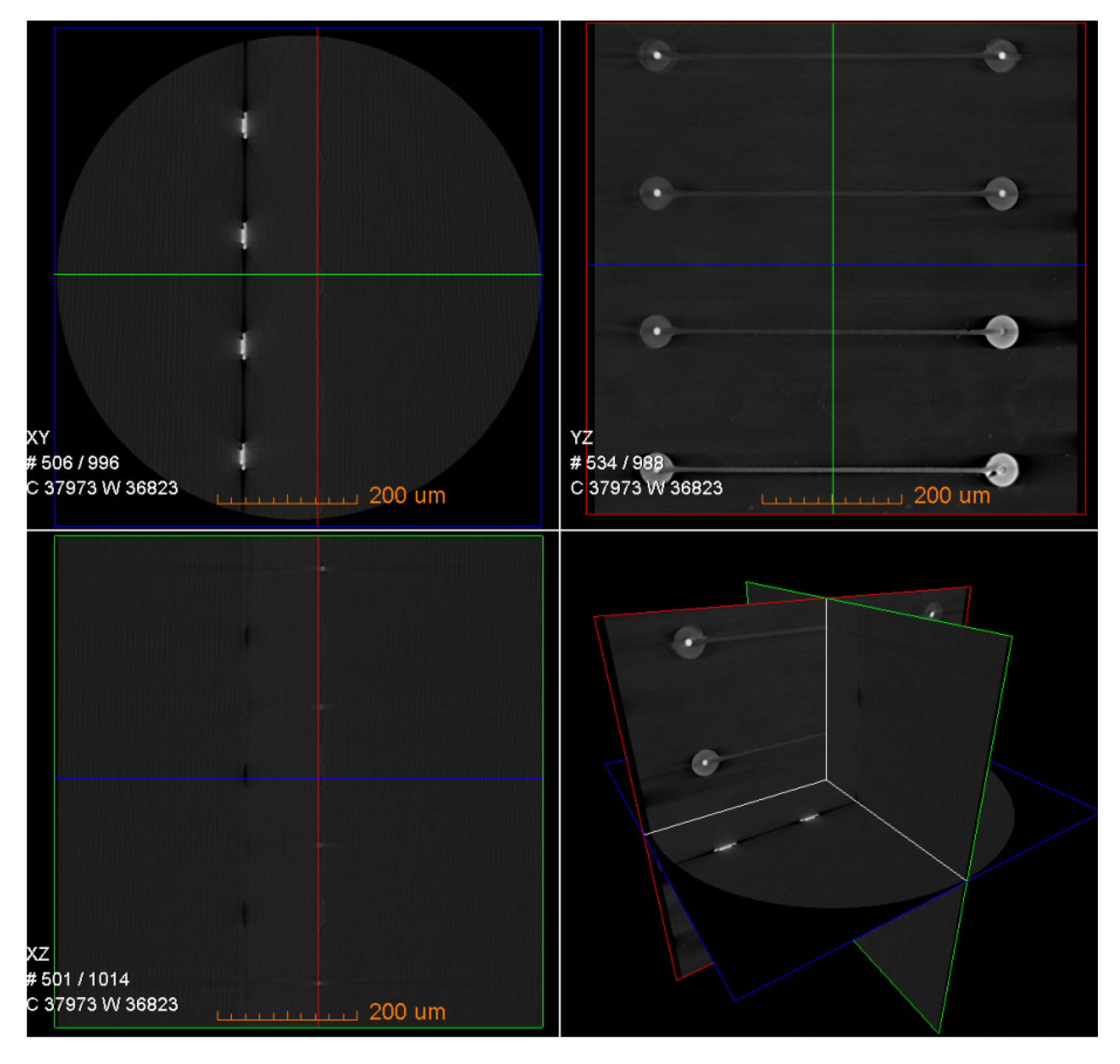
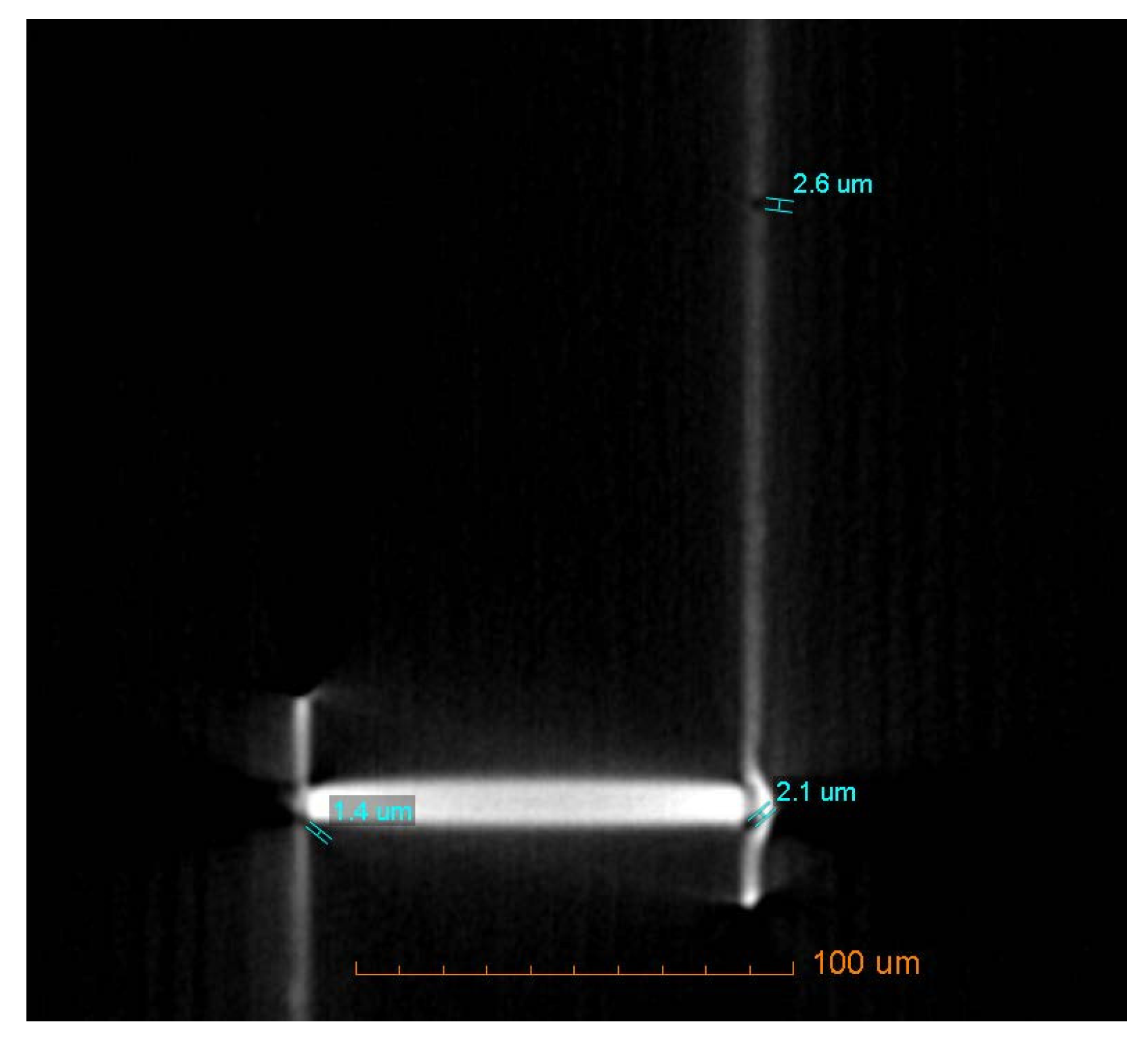
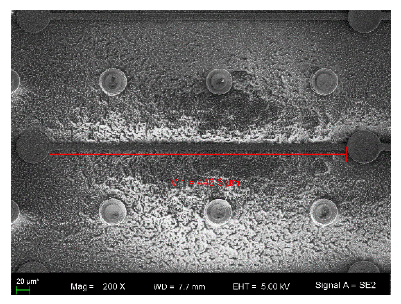
3.2. Three-Dimensional X-ray Microscopy
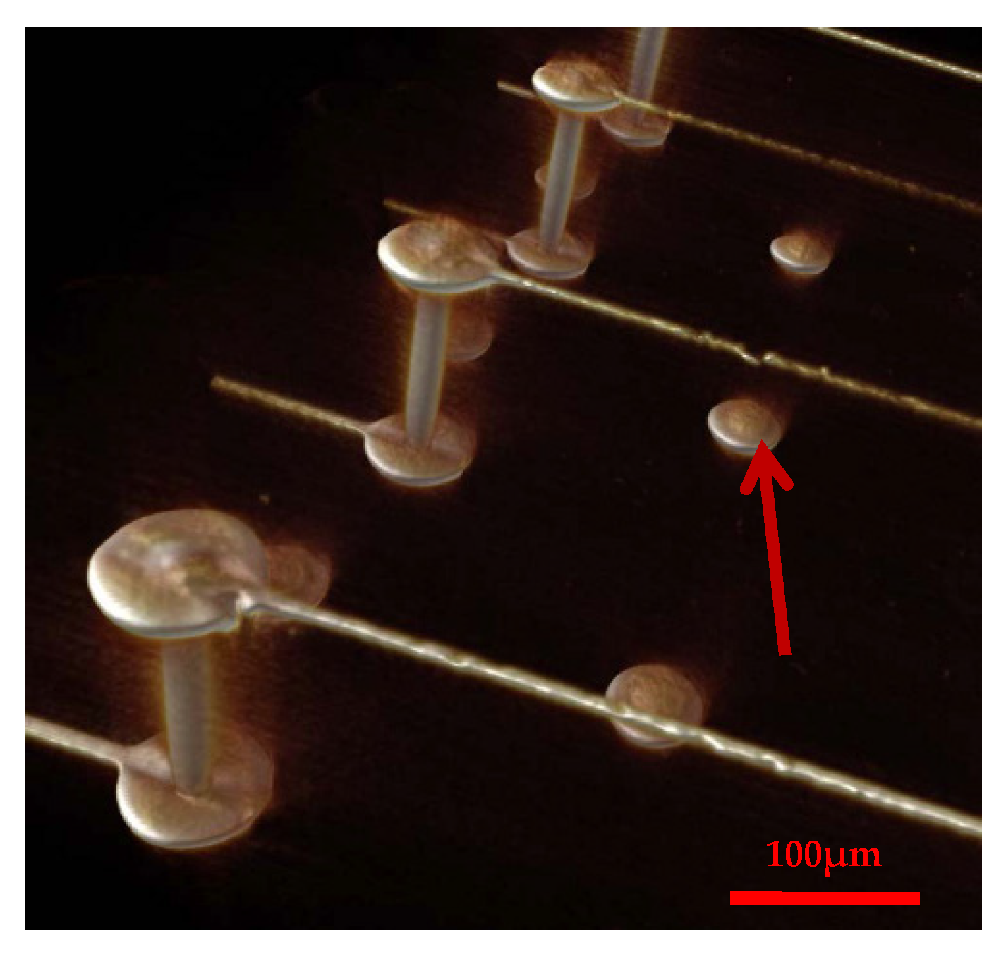
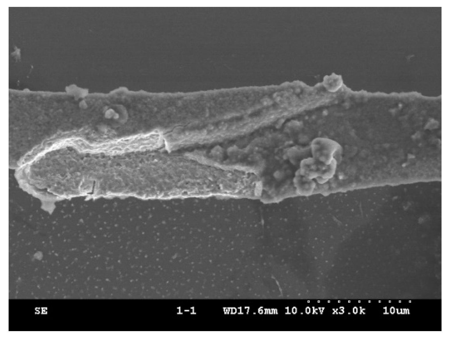
4. Physical Analysis
5. Conclusions
Author Contributions
Funding
Institutional Review Board Statement
Informed Consent Statement
Data Availability Statement
Acknowledgments
Conflicts of Interest
References
- Premachandran, C.S.; Choi, S.; Cimino, S.; Tran-Quinn, T.; Burrell, L.; Justison, P. Reliability challenges for 2.5D/3D integration: An overview. In Proceedings of the IEEE International Reliability Physics Symposium (IRPS), San Francisco, CA, USA, 11–15 March 2018. [Google Scholar]
- Shen, W.W.; Chen, K.N. Three-dimensional integrated circuit (3D IC) key technology: Through-silicon via (TSV). Nanoscale Res. Lett. 2017, 12, 56–59. [Google Scholar] [CrossRef] [PubMed] [Green Version]
- Jung, D.H.; Kim, Y.; Kim, J.J.; Kim, H.; Choi, S.; Song, Y.-H.; Bae, H.-C.; Choi, K.-S.; Piersanti, S.; De Paulis, F. Through Silicon Via (TSV) Defect Modeling, Measurement, and Analysis. IEEE Trans. Compon. Packag. Manuf. Technol. 2017, 7, 138–152. [Google Scholar] [CrossRef]
- Premachandran, C.; Tran-Quinn, T.; Burrell, L.; Justison, P. A Comprehensive Wafer Level Reliability Study on 65nm Silicon Interposer. In Proceedings of the IEEE International Reliability Physics Symposium (IRPS), Monterey, CA, USA, 31 March–4 April 2019. [Google Scholar]
- Chan, J.M.; Lee, K.C.; Tan, C.S. Effects of Copper Migration on the Reliability of Through-Silicon via (TSV). IEEE Trans. Device Mater. Reliab. 2018, 18, 520–528. [Google Scholar] [CrossRef]
- de Wolf, I.; Croes, K.; Beyne, E. Expected Failures in 3-D Technology and Related Failure Analysis Challenges. IEEE Trans. Compon. Packag. Manuf. Technol. 2018, 8, 711–718. [Google Scholar] [CrossRef]
- Jung, H.D.; Kim, H.; Kim, J.J.; Kim, S.; Kim, J.; Bae, H.-C.; Choi, K.-S. Fault detection and isolation of multiple defects in through silicon via (TSV) channel. In Proceedings of the IEEE International 3D Systems Integration Conference (3DIC), Cork, Ireland, 1–3 December 2014. [Google Scholar]
- Brand, S.; Altmann, F. Lock-In-Thermography, Photoemission, and Time-Resolved GHz Acoustic Microscopy Techniques for Nondestructive Defect Localization in TSV. IEEE Trans. Compon. Packag. Manuf. Technol. 2018, 8, 735–744. [Google Scholar] [CrossRef]
- Jacobs, K.J.P.; Li, Y.; Stucchi, M.; De Wolf, I.; Van Huylenbroeck, S.; De Vos, J.; Beyne, E. Optical Beam-Based Defect Localization Methodologies for Open and Short Failures in Micrometer-Scale 3-D TSV Interconnects. IEEE Trans. Compon. Packag. Manuf. Technol. 2020, 10, 1542–1551. [Google Scholar] [CrossRef]
- Gaudestad, J.; Nuez, D.; Tan, P. Short Localization in 2.5D Microchip with Interposer using Magnetic Current Imaging. In Proceedings of the 40th International Symposium for Testing and Failure Analysis American Society for Metals, Houston, TX, USA, 9–13 November 2014. [Google Scholar]
- Liu, C.Y.; Kuo, P.S.; Chu, C.H.; Gu, A.; Yoon, J. High resolution 3D X-ray microscopy for streamlined failure analysis workflow. In Proceedings of the IEEE 23rd International Symposium on the Physical and Failure Analysis of Integrated Circuits (IPFA), Singapore, 18–21 July 2016. [Google Scholar]
- Krause, M.; Altmann, F.; Schmidt, C.; Petzold, M.; Malta, D.; Temple, D. Characterization and failure analysis of TSV interconnects: From non-destructive defect localization to material analysis with nanometer resolution. In Proceedings of the IEEE 61st Electronic Components and Technology Conference, Lake Buena Vista, FL, USA,, 31 May–3 June 2011. [Google Scholar]
- Schmidt, C.; Lechner, L.; de Wolf, I.; Kim, S.; Beyne, E. Novel Failure Analysis Techniques for 1.8 µm Pitch Wafer-to-Wafer Bonding. In Proceedings of the IEEE 68th Electronic Components and Technology Conference (ECTC), San Diego, CA, USA, 29 May–1 June 2018. [Google Scholar]
- Oravec, M.; Pačaiová, H.; Ižaríková, G.; Hovanec, M. Magnetic Field Image—Source of Information for Action Causality Description. In Proceedings of the IEEE 17th World Symposium on Applied Machine Intelligence and Informatics (SAMI), Herl’any, Slovakia, 24–26 January 2019. [Google Scholar]
- Jakubas, A. Diagnostics of the Fe-based composites using a magnetic field camera. In Proceedings of the Progress in Applied Electrical Engineering (PAEE), Koscielisko, Poland, 17–21 June 2019. [Google Scholar]
- Vallett, D.P. A Comparison of Lock-in Thermography and Magnetic Current Imaging for Localizing Buried Short-Circuits. In Proceedings of the 37th International Symposium for Testing and Failure Analysis (ISTFA), San Jose, CA, USA, 13–17 November 2011. [Google Scholar]
- Gaudestad, J.; Talanov, V.; Huang, P.C. Space Domain Reflectometry for opens detection location in microbumps. Microelectron. Reliab. 2012, 52, 2123–2126. [Google Scholar] [CrossRef]
- Wikswo, J.P. Chapter the Magnetic Inverse Problem for NDE. In SQUID Sensors: Fundamentals, Fabrication and Applications; Weinstock, H., Ed.; Kluwer Academic Publishers: New York, NY, USA; Springer: Dordrecht, The Netherlands, 1996; pp. 629–695. [Google Scholar]
- Orozco, A. Magnetic Field Imaging for Electrical Fault Isolation. In Microelectronics Failure Analysis Desk Reference; Richard, J.R., Ed.; ASM International: New York, NY, USA, 2004; pp. 303–311. [Google Scholar]
- Gaudestad, J.; Talanov, V.; Gagliolo, N.; Orozco, A. Space Domain Reflectometry for open failure localization. In Proceedings of the 19th International Symposium Physical &Failure Analysis of Integrated Circuits (ISTFA), Phoenix, AZ, USA, 11–15 November 2012. [Google Scholar]
- Murugesan, M.; Takeuchi, A.; Fukushima, T.; Koyanagi, M. X-ray computed tomography studies on directed self-assembly formed vertical nanocylinders containing metals for 3D LSI applications-characterization technique-dependent reliability issues. J. Appl. Phys. 2019, 58, SBBC05-1–SBBC05-6. [Google Scholar] [CrossRef]
- Mohammad-Zulkifli, S.; Zee, B.; Thomas, G.; Gu, A.; Yang, Y.; Masako, T.; Lee, W. High-resolution 3D X-ray Microscopy for Structural Inspection and Measurement of Semiconductor Package Interconnects. In Proceedings of the IEEE 26th International Symposium on Physical and Failure Analysis of Integrated Circuits (IPFA), Hangzhou, China, 2–5 July 2019. [Google Scholar]
- Favata, J.; Shahbazmohamadi, S. Realistic non-destructive testing of integrated circuit bond wiring using 3-D X-ray tomography, reverse engineering, and finite element analysis. Microelectron. Reliab. 2018, 83, 91–100. [Google Scholar] [CrossRef]
- Yung, L.C. Investigation of the solder void defect in IC semiconductor packaging by 3D computed tomography analysis. In Proceedings of the IEEE 20th Electronics Packaging Technology Conference (EPTC), Singapore, 4–7 December 2018. [Google Scholar]
- Hartfield, C.; Schmidt, C.; Gu, A.; Kelly, S.T. From PCB to BEOL: 3D X-Ray Microscopy for Advanced Semiconductor Packaging. In Proceedings of the IEEE International Symposium on the Physical and Failure Analysis of Integrated Circuits (IPFA), Singapore, 16–19 July 2018. [Google Scholar]
- Spinella, L.; Jiang, T.; Tamura, N.; Im, J.; Ho, P.S. Synchrotron X-Ray Microdiffraction Investigation of Scaling Effects on Reliability for Through-Silicon Vias for 3-D Integration. IEEE Trans. Device Mater. Reliab. 2019, 19, 568–571. [Google Scholar] [CrossRef] [Green Version]
- Altmann, F.; Brand, S.; Petzold, M. Failure Analysis Techniques for 3D Packages. In Proceedings of the IEEE International Symposium on the Physical and Failure Analysis of Integrated Circuits (IPFA), Singapore, 16–19 July 2018. [Google Scholar]
- Khosravani, M.R.; Reinicke, T. On the Use of X-ray Computed Tomography in Assessment of 3D-Printed Components. J. Nondestruct. Eval. 2020, 39, 1–6. [Google Scholar] [CrossRef]
- Mees, F.; Swennen, R.; van Geet, M.; Jacobs, P. Applications of X-ray Computed Tomography in the Geosciences, Geological Society London Special Publications; Geological Society: London, UK, 2003; pp. 154–196. [Google Scholar]
- Wang, Z.; Wu, Z.; Sun, J.; Duan, C. Defect Location and Physical Analysis in Chip-on-chip Device. In Proceedings of the 2019 IEEE 26th International Symposium on Physical and Failure Analysis of Integrated Circuits (IPFA), Hangzhou, China, 2–5 July 2019. [Google Scholar]
- Gourikutty, S.B.N.; Chow, Y.M.; Alton, J.; Umralkar, R.B.; Bai, H.; Chua, K.K.; Bhattacharya, S. Defect Localization in Through-Si-Interposer Based 2.5D ICs. In Proceedings of the IEEE 70th Electronic Components and Technology Conference (ECTC), Orlando, FL, USA, 3–30 June 2020. [Google Scholar]
- Xu, X.; Huang, W.; Chen, Y. Failure Localization Method in Open Mode Failure Analysis of Advanced Package. In Proceedings of the 21st International Conference on Electronic Packaging Technology (ICEPT), Guangzhou, China, 12–15 August 2020. [Google Scholar]


| Channel | DC Resistance before TC (Ω) | DC Resistance after TC (Ω) |
|---|---|---|
| C1 | 6.179 | 7.925 |
| C2 | 6.584 | 2.41 × 10⁴ |
| C3 | 6.420 | 6.414 |
| C4 | 6.643 | 6.449 |
| C5 | 6.743 | 6.307 |
| C6 | 6.808 | 9.76 × 10⁷ |
| C7 | 5.994 | 5.182 |
| C8 | 5.959 | 6.397 |
| C9 | 6.437 | 6.239 |
| C10 | 6.637 | 6.455 |
| C11 | 6.492 | 6.551 |
| C12 | 6.672 | 6.615 |
| C13 | 6.634 | 1.23 × 10⁵ |
Publisher’s Note: MDPI stays neutral with regard to jurisdictional claims in published maps and institutional affiliations. |
© 2021 by the authors. Licensee MDPI, Basel, Switzerland. This article is an open access article distributed under the terms and conditions of the Creative Commons Attribution (CC BY) license (https://creativecommons.org/licenses/by/4.0/).
Share and Cite
Chen, Y.; Lai, P.; Huang, H.-Z.; Zhang, P.; Lin, X. Open Localization in 3D Package with TSV Daisy Chain Using Magnetic Field Imaging and High-Resolution Three-Dimensional X-ray Microscopy. Appl. Sci. 2021, 11, 8148. https://doi.org/10.3390/app11178148
Chen Y, Lai P, Huang H-Z, Zhang P, Lin X. Open Localization in 3D Package with TSV Daisy Chain Using Magnetic Field Imaging and High-Resolution Three-Dimensional X-ray Microscopy. Applied Sciences. 2021; 11(17):8148. https://doi.org/10.3390/app11178148
Chicago/Turabian StyleChen, Yuan, Ping Lai, Hong-Zhong Huang, Peng Zhang, and Xiaoling Lin. 2021. "Open Localization in 3D Package with TSV Daisy Chain Using Magnetic Field Imaging and High-Resolution Three-Dimensional X-ray Microscopy" Applied Sciences 11, no. 17: 8148. https://doi.org/10.3390/app11178148
APA StyleChen, Y., Lai, P., Huang, H.-Z., Zhang, P., & Lin, X. (2021). Open Localization in 3D Package with TSV Daisy Chain Using Magnetic Field Imaging and High-Resolution Three-Dimensional X-ray Microscopy. Applied Sciences, 11(17), 8148. https://doi.org/10.3390/app11178148