Article

Atmospheric Pressure Dielectric Barrier Discharge Plasma-Enhanced Optical Contact Bonding of Coated Glass Surfaces

by
Josephine Neumann
1,
Stephan Brückner
1,
Wolfgang Viöl
1,2 and
Christoph Gerhard
1,*
1
Faculty of Engineering and Health, University of Applied Sciences and Arts, Von-Ossietzky-Straße 99, 37085 Göttingen, Germany
2
Thin Films IST-Application Center for Plasma and Photonics, Fraunhofer Institute for Surface Engineering, Von-Ossietzky-Straße 100, 37085 Göttingen, Germany
*
Author to whom correspondence should be addressed.
Appl. Sci. 2021, 11(15), 6755; https://doi.org/10.3390/app11156755
Submission received: 10 June 2021 / Revised: 16 July 2021 / Accepted: 21 July 2021 / Published: 22 July 2021
(This article belongs to the Special Issue Plasma Science and Technology)

Abstract

:
This paper reports on plasma-enhanced bonding of optics surfaces coated with highly sensitive functional layers using surface preparation by a dielectric barrier discharge (DBD) plasma. The samples to be bonded were treated with a DBD in diffuse mode at atmospheric pressure for 30 s which is applied directly to the sample surface, then joined with the aid of de-ionised water and cured subsequently. The plasma treatment itself already increased the shear strength achieved by a factor of two compared to classical wringing or direct contacting, while the curing process led to a further increase by a factor of up to five, depending on curing temperature. The observed enhancement of shear strength can be attributed to DBD plasma-induced cleaning and most likely additional activation of the surface as verified by contact angle measurements. Since the impact of the used plasma on the surface is quite gentle in comparison to other bonding processes or other plasma-based processes reported in the literature, a destruction of the treated functional layer is avoided. This advantage makes it possible to bond even optics surfaces coated with sensitive materials.

1. Introduction

Joining-material-free processes for the direct contacting or connection of optically active surface components are of increasing importance due to the growing need and use of UV- and high power laser optics as well as vacuum applications. Here, the classical optical cements cannot be used due to their low laser-induced damage threshold and high UV-absorbance. The common method to generate direct contacted optical components without such cement is wringing, also known as optical contact bonding [1]. This method originates from the manufacturing process of optics with high demands on surface form deviation or angularity. In the optical manufacturing process, wringing is usually applied for the temporary attachment of optical components to manufacturing tools made of glass. Physically, the effect of wringing can be based on intermolecular phenomena [2] such as dipole–dipole or van-der-Waals forces [3] on the one hand and a thin water film and capillary forces on the other hand [4]. Due to the different expansion coefficients of different glasses, such an attachment can be easily released by heating. In addition to temperature fluctuations, environmental influences in the form of vibrations can also lead to loosening of the connection. Hence, such wringing is basically not suitable to generate permanently contacted optics.
To realise the permanent attachment of uncoated optical components all the same, processes based on the methods used in the semiconductor industry for direct wafer bonding are modified to optics made of glass. The direct bonding processes consists of the three process steps surface activation, merging and curing. Surface activation during direct bonding of wafers is either performed wet-chemically—for example by using ammonium hydroxide, hydrogen peroxide and water—or physically by plasma treatment at low pressure [5,6]. After surface activation, the wafers are brought into contact and an annealing process is performed to generate covalent bonds. For annealing of silica wafers, temperatures of approx. 1100 C are reached [7] since, at such temperatures, the silanol groups that perform the actual covalent bond between bonded components reaches the highest stability [8]. At lower annealing temperatures, wet chemical activation and plasma activation can also be combined to obtain high bond stability [9].
For direct bonding of optics, this bonding process can also be performed after slight modifications mainly concerning the annealing temperature. For surface activation of uncoated optics, there are already different wet-chemical procedures established in optics manufacturing [10]. Similar to the bonding of wafers, a dilution of ammonium hydroxide, hydrogen peroxide and water [11] or a dilution of potassium hydroxide and water can be applied [12]. Furthermore activation can be achieved by plasma treatment [13]. Fused silica and borosilicate glasses were already bonded successfully after surface activation via a dielectric barrier discharge (DBD) plasma treatment at atmospheric pressure and a subsequent annealing process [14]. The transfer of bonding technologies used for wafers and uncoated optics or glass surfaces to optical components with functional coatings is of great interest. Such direct contacting of coated elements would represent an added value for optics manufacturing. Due to the temperature sensitivity of functional coatings the annealing temperatures are lowered to a range of 100 C up to 250 C [11,14]. The wet-chemical processes were already performed successfully on optical components with dielectric functional coatings, whereas the use of the plasma process has turned out to be problematic due to the fact that the used DBD penetrates into the coating material [15,16]. For optical components coated with functional layers such as non-polarising beam splitters, which usually contain metal, wet-chemical bonding procedures are not applicable because the functional layers are destroyed. Here, plasma-based processes have turned out to be promising alternative techniques [17]. Different types of cold atmospheric pressure plasmas were taken into account for the activation of this type of coated surface. When applied directly to the sample surface, filamentary DBDs in various configurations [18,19] as well as sliding discharges [19] damage the functional layer even when they are operated at low voltages directly at the ignition limit. The coating contains a thin metal layer and thus favours the emergence of relatively high-current filaments that cause the destruction through all coating layers. This could also be observed for DBD-based jet plasmas. Moreover, particles were observed on the optical functional layers which originate from the ambient air and are carried onto the surface by the gas flow. Therefore, the filamentary DBDs and the DBD-based jet plasmas are unsuitable for the treatment of sensitive optical functional layers due to their discharge properties. However, DBDs can also be operated in diffuse [18] or also called quasi-homogenous mode depending on the duration of the exciting high-voltage pulses [20], the general configuration of the plasma source and the process gas. In this mode, gentle surface preparation comparable to treatments by glow discharges can be achieved. Moreover, treatment of glass surfaces in this mode is most probably highly effective [21] and was already performed successfully for glass surfaces [22,23]. Furthermore, DBDs offer the advantage of easy handling since no vacuum equipment and periphery are required.
In previous works, such plasmas have also been investigated for quite different applications in optics manufacturing. This includes the improvement in adhesiveness of classically cemented optics [24], surface cleaning [25], e.g., for increasing the laser-induced damage threshold [26], and polishing of optical glasses and media [27]. Against this background, demonstrating the exceptional high potential of DBDs at atmospheric pressure in the production of precision optics, the suitability of plasmas for the enhancement of optical contact bonding processes was investigated in the present work.

2. Materials and Methods

2.1. Investigated Samples

The samples used in this work were circular blanks made of fused silica (Spectrosil 2000 from Heraeus) with a diameter of 25 mm and a thickness of 5 mm. The samples were produced by classical optical manufacturing techniques. For polishing, a plane polishing tool with a polishing pad made of polyurethane and a premixed water-based polishing suspension (Hastilite PO from Universal Photonics, Inc., New York, NY, USA) were used. The surface accuracy was λ / 10 , corresponding to 0.2 Newton fringes, while the surface roughness was Rq < 0.5 nm as determined via an interferometer over a spatial bandwidth of 1 μ m–300 μ m.
First the bonding process was tried out with pairs of uncoated samples. For the following investigation, an uncoated blank and a coated one were bonded where two different coatings were tested: first, a metal-containing non-polarising beam splitter (NPBS) coating consisting of silicon dioxide (SiO 2 ), niobium pentoxide (NbO 5 ) and silver (Ag) and second, a pure dielectric polarising beam splitter (PBS) coating made of niobium pentoxide and silicon dioxide. The outermost protection layer of both coatings is made of silicon dioxide where the layer thickness is higher in the case of the NPBS coating.

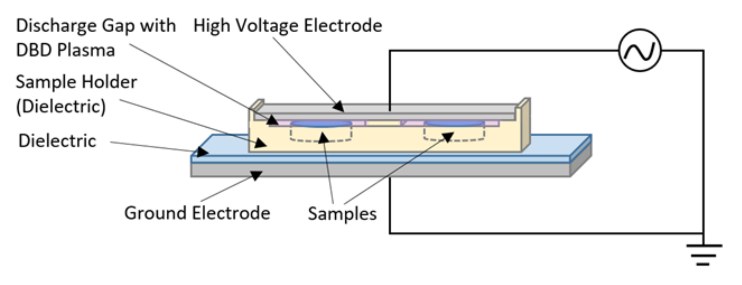
2.2. Experimental Setup and Testing

For plasma treatment, a plasma source with a flat copper electrode and an alumina-silicate glass plate as dielectric separation was used. As shown in Figure 1, the samples were placed in a plastic housing made of photopolymer resin. The plasma was ignited between the high-voltage electrode and an external ground electrode located below the housing. The purpose of the dielectric on the ground electrode is to mitigate accidental flashovers in the laboratory setup. The 1 mm wide discharge gap was flushed with the process gas. The used input gases were synthetic air, nitrogen (N 5.0), argon (Ar 5.0) and helium (He 5.0; each was from Linde Gas AG). All used process gases contained a small proportion of approx. 0.5% ambient air, resulting from the intended final use in ambient air in classical optics production without an additional enclosure. The gas flow rate was 5 L per minute since the highest plasma homogeneity was achieved at this setting.
Due to the dielectric separation, a direct DBD plasma was ignited. As is common for DBD plasmas, an alternating high voltage was applied to power the discharge. The voltage pulses are generated according to the Fourier synthesis principle. The chosen peak voltage as well as the pulse repetition rates depended on the ignition threshold of the used process gases and their respective behaviour concerning the formation of stationary filaments. In general, the voltages were chosen to be as low as possible for each process gas to allow plasma ignition on the one hand and to avoid layer destruction on the other hand. Due to the different ignition voltages of the various process gases, all plasmas operated at different voltages. Since they are all used directly near their respective ignition limit, a comparison is nevertheless useful for the intended application. The different current–voltage characteristics are shown in Figure 2. For each of the different process gases, the mean power was determined using the Electric Current method from [28]. The mean powers, together with the respective amplitudes, pulse repetition rates, voltages and currents are shown in Table 1. The pulse duration of each high-voltage pulse was about 1 μ s (FWHM). Since DBD plasmas feature low gas temperatures [20], the maximum observed sample temperature was 23 C.
The plasmas using the different process gases were first applied to the functional NPBS-layer containing silver, as this is the most sensitive coating. Microscope images were taken to check whether the plasma treatment causes coating damage. Moreover, contact angle measurements were carried out to detect whether plasma-induced surface conditioning already occurs before coating damage. Using this setup with helium as process gas enables both the highest homogeneity of the plasma and the gentlest surface conditioning, contact angle measurements were performed to determine the optimal treatment time. Due to better contrast, those measurements were performed on uncoated samples. Since both coatings have a silicon dioxide top layer, no differences are to be expected between coated and uncoated samples. Bond tests were then carried out with the parameters determined in that vein.
In order to investigate the impact of such plasma treatment on the stability of bonded doublets, pairs of uncoated and uncoated or uncoated and coated samples were brought into direct contact and pressed at a mechanical pressure of 0.2 MPa. Such contacting was performed in deionised and distilled water. This approach is the standard wringing process in optics manufacturing since it allows for a final fine adjustment of the components after contacting due to the thin water film between the surfaces. Moreover, it helps to meet the cleanliness requirements of the optics industry. Subsequently, the samples were cured at different temperatures in order to remove this water film. The curing temperatures were 100 C and 200 C, respectively, depending on the temperature resistance of the coating. The curing duration was 120 h. For comparison, a set of samples was additionally stored at an ambient temperature of approximately 22 C. This corresponds to the reference process, classical contact bonding [1].
In order to investigate the influence of the plasma treatment on the stability of bonded optical components, 20 of each different combinations, i.e., different uncoated/uncoated and coated/uncoated samples were bonded and subsequently tested. For this purpose, the shear strength was measured via a blade test as principally described in [7]. In contrast to this approach, the force required to completely separate the bonded samples was measured. Moreover, the impact of plasma treatment on the contact angle of diiodmethane on fused silica surfaces was measured. The measurement was performed with a contact angle measurement system (Mobile Surface Analyzer from Krüss).

3. Results

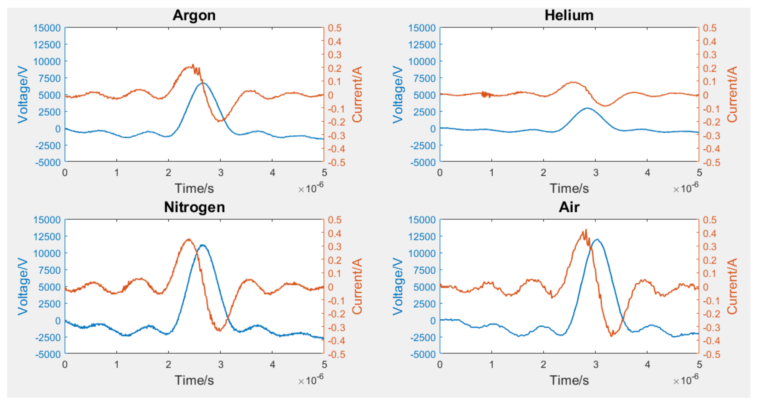
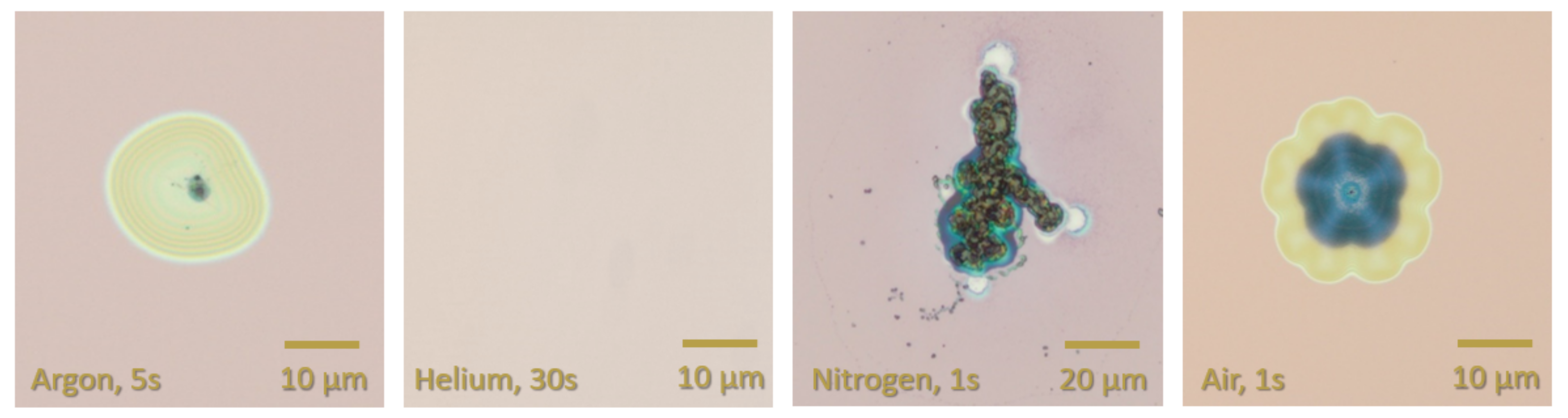
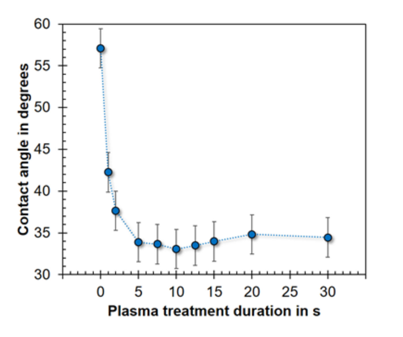
3.1. Determination of the Suitable Preparation Parameters of Coated Surfaces
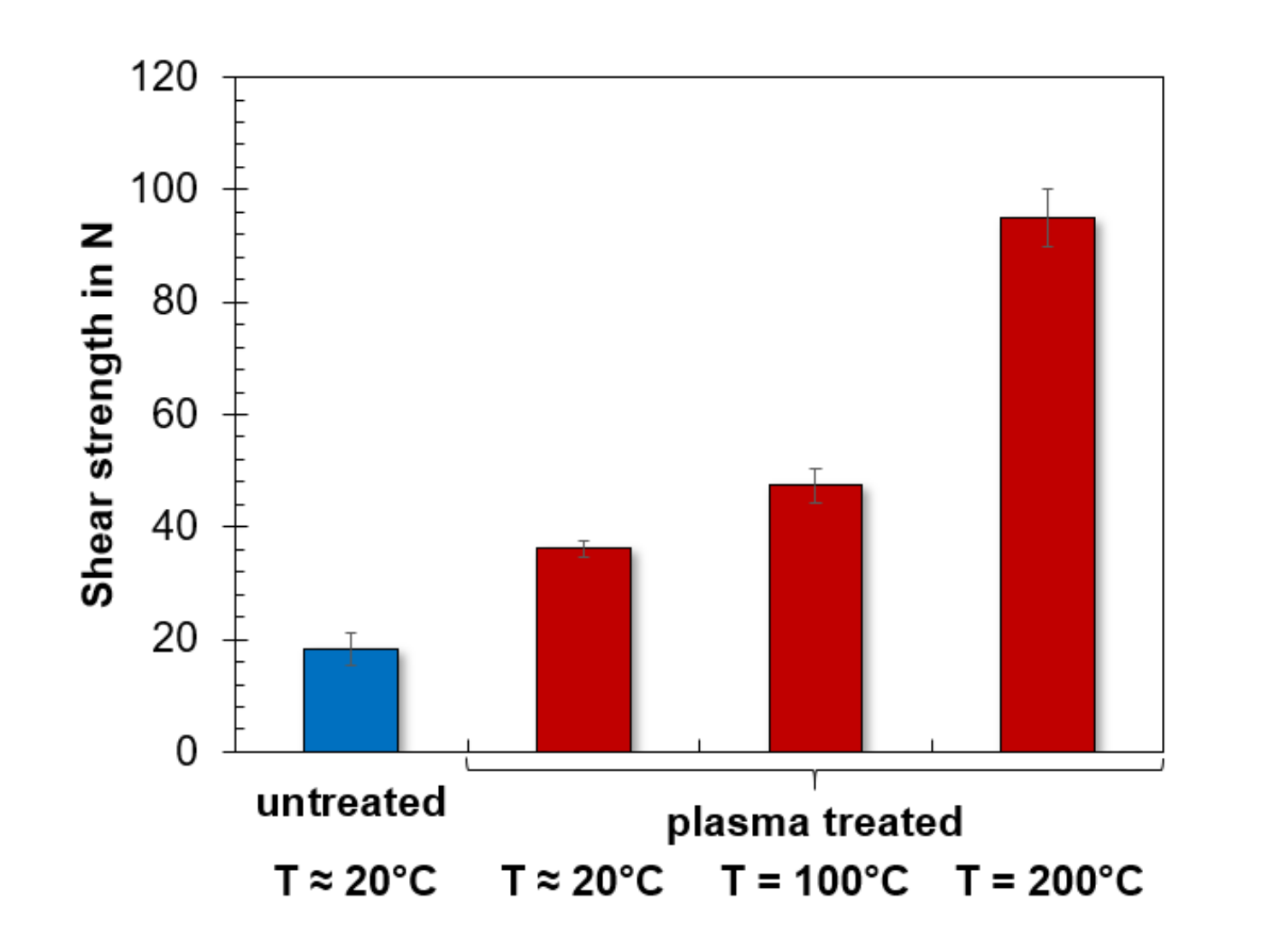
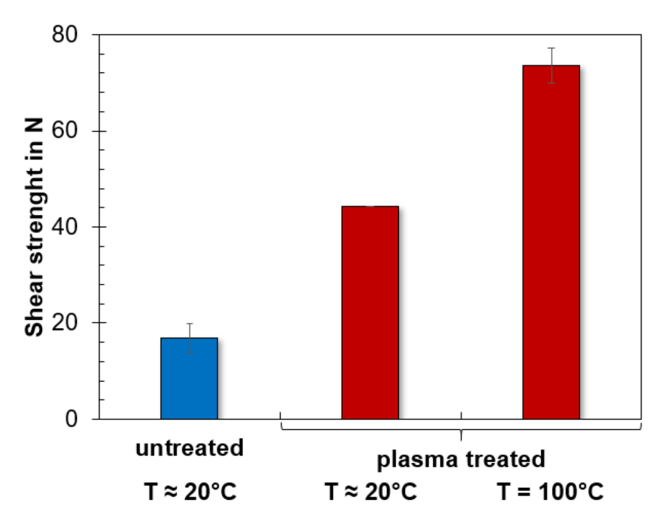
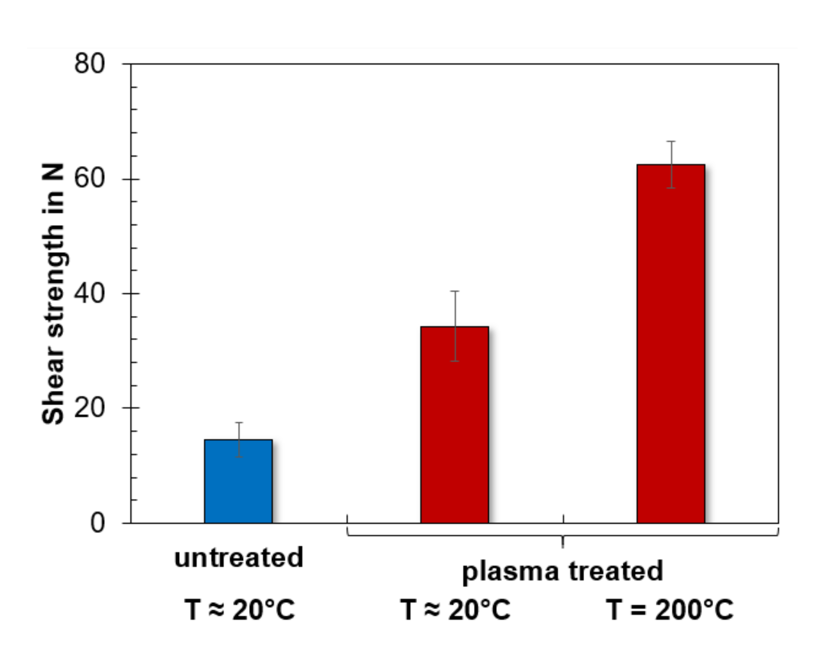
Initially, the particular process gas-dependent treatment times leading to first breakdowns of an NPBS coating during DBD plasma treatment were determined. For argon, the first layer destructions occurred between 2 s and 5 s, so the treatment time must not exceed 2 s. The contact angle reached at this time was 34.7 , starting at a reference value of 57.1 where the test liquid was diiodmethane. For both nitrogen and air visible destruction already appeared after a 1 s treatment duration. For this reason, these gases are not suitable for surface preparation of the investigated coatings and no contact angle measurement was performed. The use of helium plasma allows a treatment time of up to one minute without any damage to the functional layer. Figure 3 shows microscope images of the layer defects that could be observed after the different treatment durations.
In Figure 4, the diiodmethane contact angle of a sample surface treated with a helium DBD is plotted versus the treatment time. The contact angle is notably decreased after plasma treatment. The water contact angle was not measurable any more for very short treatment durations, i.e., 1–2 s, showing the high degree of hydrophilisation induced by the plasma. Hence, diiodmethane instead of de-ionised water was used as test liquid. After a duration of 30 s, the contact angle is approximately 1.7 times lower in comparison to the untreated surface. As can be seen in Figure 4, the significant decrease in the contact angle already stops after 5 s. At this point, the contact angle achieved is 33.9 .
Based on the results obtained by the microscope images shown in Figure 3 and the contact angle measurements, a helium plasma with a treatment time of 30 s was used for further sample treatment. The preparation time of 30 s was chosen to provide the maximum treatment and to avoid any possible layer destruction, which can occur for treatment durations above 60 s at the same time. The contact angle is already stable at this point and no coating damage is risked by further approaching the limit of treatment duration of 60 s. Helium instead of argon was selected, since with argon plasma a very slight overrun of the treatment time already leads to coating damage in the NPBS coating. In addition, the contact angle is not yet stationary after a treatment time of 2 s.

3.2. Bonding Tests

In order to demonstrate the impact of the applied plasma treatment on the stability of bonded glass components, uncoated fused silica samples were tested initially. As shown in Figure 5, the shear strength was generally increased by the plasma treatment. With respect to the untreated reference which was cleaned by hand according to the common standards of optics manufacturing and wringed, this increase can be quantified by a factor of about two in the case of storing the bonded doublet at ambient temperature. The stability is further increased by curing at higher temperatures. Here, the shear strength was 2.6 times and 5.2 times higher after curing at 100 C and 200 C, respectively. The general increase in shear-strength can be attributed to a plasma-induced modification of the glass surface shown in Figure 5.
Since the outermost layer of both investigated coatings of interest, NPBS and PBS, basically consist of silicon dioxide, the observed increase in shear strength is also to be expected in the case of coated optics as presented in the subsequently. Here, the goal was to achieve the highest possible stability. Figure 6 shows the shear strengths of bonded doublets coated with the NPBS coating described in Section 2.1. As observed for uncoated optics (Figure 5), the plasma treatment resulted in an increase in shear strength. The maximum possible curing temperature was 100 C since the NPBS coating was damaged at higher temperatures due to the involved silver.
With respect to the untreated reference (cleaned and wringed according to optics manufacturing standards), the plasma treatment caused an increase in shear strength by a factor of 2.6 after storing at ambient temperature and 4.8 after curing at 100 C. A quite comparable behaviour was observed for doublets coated with the PBS coating, see Figure 7.
Here, the shear strength was increased by a factor of 2.3 and 4.3 due to storing at ambient temperature and curing at 200 C, respectively. Even though here a higher curing temperature could be applied since the coating does not contain any metallic components, the plasma-induced increase is in the same order of magnitude as for NPBS-coated optics.

4. Discussion

The results presented in Figure 3 show that the applied diffuse DBD plasma using helium as process gas allows the treatment of NPBS coatings without layer destruction. It is crucial that the DBD is in a diffuse mode with as few stationary filaments as possible. The generation of a diffuse DBD after [21,23] can be made possible by the appropriate choice of electrode geometry. Diffuse DBDs can activate surfaces simultaneously in a particularly gentle but highly effective manner [22]. The influence of different process gases on the homogeneity of the DBD can be seen in Figure 2 in the current curves. For the helium DBD, the current curve is the smoothest, which indicates the highest homogeneity. The positive influence of helium on plasma homogeneity has already been observed in [29,30] where a homogeneous DBD at atmospheric pressure was produced with helium as process gas. The stationary filaments of the current curves of the other investigated gases are very pronounced and have a greater power density due, among other things, to the higher applied voltage than for helium. Thus, such filaments lead to the destruction of the NPBS functional layer for all gases except helium. As the contact angle measurements show, significant modification of the surfaces takes place. With the presented approach, a surface conditioning for bonding of very sensitive optical functional layers becomes possible.
In Figure 5, Figure 6 and Figure 7 an increase in shear strength only induced by plasma treatment could be observed. The influence of the plasma treatment on the surface is also reflected in the contact angle measurement shown in Figure 4. As can be seen there, the plasma affects the surface very quickly. After 5 s, the occurrence of saturation can already be observed. After this, the variation of values of the contact angle measurement takes place only in the range of the standard deviation. The increase in shear strength and the decrease in the contact angle can be explained by plasma-induced cleaning. In addition, the occurrence of surface activation is probable. The rapid decline of contact angle indicates a very superficial contamination in the area of a few atomic layers. This contamination may come from the storage period of the optics after manufacturing, even under clean conditions. Thus, small amounts of carbon and hydrocarbons can accumulate on the surface. This type of contamination forms in a short time due to the storage of optics and cannot be removed by manual cleaning with acetone or ethanol. Plasma treatment removes such carbon groups [25] and may furthermore remove residues of the used polishing agent [26], which is adsorbed on the surface and also cannot be removed by classical manual cleaning that is applied in optics manufacturing. This leads to an increase in surface energy, which is reflected by a decrease in the measured contact angle. The removal of carbon groups also shifts the ratio of oxygen present at the surface from the siloxane bonds of the fused silica surface and attached carbons. In [31], a direct relationship between the oxygen–carbon ratio and the contact angle was demonstrated. It is most likely that this relationship also applies to the glass samples here as indicated by the contact angle measurement shown in Figure 4.
It is known from the literature [8,32] that plasma treatment of Silicon dioxide surfaces has both cleaning and activation effects. It is likely that such an activation effect contributes to the achievement of bond strength. This should be investigated as part of further work. As in chemical activation, e.g., by RCA-SC1, the siloxane bonds located on the surface are broken, and other functional groups, such as hydroxyl or amino groups [8,11], attach to the open bonds according to the environment in which the activation takes place.
As already described in other work [8] and shown in Figure 5, Figure 6 and Figure 7 an increase in shear strength caused by the annealing process can be stated, which is a quite well known effect. While after plasma treatment and curing at room temperature the shear strength increased by a factor of two, after performing the annealing process it increased again. For uncoated optics the shear strength increased with increasing annealing temperature as can be seen in Figure 5. The NPBS-coated optics reached a higher shear strength with an annealing temperature of 100 C than PBS-coated optics does with an annealing temperature of 200 C. One explanation for this is the greater overall layer thickness of the PBS coating and its material selection. This combination can lead to the formation of layer stresses, which worsen the adhesion of the layer to other surfaces during bonding or optical contacting. Moreover, the particular temperature-dependent increases do not confirm the results observed for untreated fused silica. This behaviour could be attributed to differences in composition of the outermost and thus contacting surfaces: in the case of coated optics, a high purity of the deposited silicon dioxide layers is achieved. Classically polished fused silica surfaces are used for the preliminary investigations; however, they feature a significantly different chemical composition of the near-surface material. In the course of the manufacturing process, residues from the used tools and operating materials such as polishing agents are implanted into the surface [33,34,35,36] where the lateral distribution of such contaminants can even be strongly inhomogeneous [37]. As a result, the impact of plasma treatment is most likely different for coated surfaces on the one hand and uncoated, polished surfaces on the other hand. Moreover, differences in cleanliness of the initial surfaces may further contribute to different efficiencies of plasma treatment.
The process developed and reported here offers the possibility of bonding even very sensitive surfaces such as functional coatings gently and permanently without joining materials. In order to further expand the application possibilities, the transferability of the process to other coatings and layers should be investigated in further studies. Furthermore, with regard to material compatibility, it should be investigated whether the process can be transferred from planar optics to spherical optics such as achromatic doublets. When transferring the method, the different expansion coefficients of the involved glasses must be taken into account, which can lead to loosening of the bond during the curing process. If the process can be transferred to other glass materials and even to different glass pairs, it creates quite a number of new possibilities in optics manufacturing. Finally, it should be noted that the bond surfaces were additionally inspected for defects using microscopy and spectroscopy. No significant defects that would impair the use of the plasma-treated and bond optics were found across all samples. Since the surfaces are in specification with respect to the requirements for cemented optics, the presented approach fulfils its intended purpose of offering an alternative solution to the classical cementing process.

5. Conclusions

This paper is the first to describe a method for bonding optics with sensitive metal containing functional coatings. It thus opens up new possibilities in the production of high-precision beam splitter optics. It is based on surface activation by diffuse helium DBD of high homogeneity. The applied plasma treatment leads to an increase in the achieved bond strengths by a factor of approximately two compared with untreated, classically contacted samples. This fits with the observations of the contact angle measurement that for both polar liquids (water) and predominantly disperse ones (diiodomethane) the contact angle decreases and thus the wettability and bond strength increases. The described increase in shear strength and decrease in contact angle in the manner shown due to plasma treatment is observed in an almost identical manner for uncoated and coated/uncoated specimen pairs. This can be attributed to the same basic surface material (silicon dioxide) of all samples used. The shown behaviour of the samples allows the conclusion that the sample surface is at least cleaned and possibly also activated by the plasma treatment.
Thermal treatment as part of the annealing process further increases the bond strength achieved, with this increasing in proportion to the increase in temperature. This indicates that the surfaces are activated by the plasma treatment and that the siloxane bonds described in the introduction, whose strength increases with temperature, are formed as a result of the curing process. This means that a bond can be said to be formed. The differences in the strength measurements carried out on the various coated samples can be attributed to the layer properties and the resulting layer stresses.
Even though it was demonstrated that the presented approach allows for notable increase in bonding strength of optics surfaces with functional coatings further investigations are to be performed in ongoing work. This includes the characterisation of the impact of the plasma treatment on surface roughness and waviness, adhesion energy as well as the chemical composition of the surface and surface-adherent groups. Such investigations are to be performed in order to identify the most important mechanisms such as cleaning or surface activation that contribute to the observed increase in bond strength.

Author Contributions

J.N. conceived and designed the experiments, prepared the samples, performed the experiments, analysed the data, and wrote and edited the paper draft; S.B. supervised the experiments, validated the obtained results and reviewed and edited the paper draft; W.V. acquired the funding and administrated the project and reviewed and edited the paper draft; C.G. conceived the experiments, visualised the obtained data and wrote and edited the paper draft. All authors have read and agreed to the published version of the manuscript.

Funding

The support by the Federal Ministry of Education and Research in the frame of the FH-Impuls partnership “Plasma for Life”, grant number 13FH6I02IA is gratefully acknowledged.

Institutional Review Board Statement

Not applicable.

Informed Consent Statement

Not applicable.

Data Availability Statement

Raw data are available on request.

Acknowledgments

The authors thank Qioptiq Photonics GmbH & Co.KG for providing the investigated samples. Further, the authors thank Thomas Thöniss, Martin Bischoff and Cornelia Wüstefeld from Qioptiq Photonics GmbH & Co.KG for supporting this work and preparing samples for the bond tests.

Conflicts of Interest

The authors declare no conflict of interest. The funders had no role in the design of the study; in the collection, analyses, or interpretation of data; in the writing of the manuscript, or in the decision to publish the results.

References

  1. Haisma, J.; Spierings, G.A.C.M. Contact bonding, including direct-bonding in a historical and recent context of materials science and technology, physics and chemistry. Mater. Sci. Eng. 2002, 37, 1–60. [Google Scholar] [CrossRef]
  2. Smith, H.I. Optical-Contact Bonding. J. Acoust. Soc. Am. 1965, 37, 928–929. [Google Scholar] [CrossRef]
  3. Greco, V.; Marchesini, F.; Molesini, G. Optical contact and van der Waals interactions: The role of surface topography in determining the bonding strength of thick glass plates. J. Opt. A 2001, 3, 85–88. [Google Scholar] [CrossRef]
  4. Homayouini, S.M.; Vasili, M.R.; Hong, T.S. Bonding Technbologies in Manufacturing Engineering. In Somprehensive Materials Processing; Saleem, H., Ed.; Elsevier Science: Amsterdam, The Netherlands, 2014; pp. 237–246. [Google Scholar]
  5. Farrens, S.N.; Dekker, J.R.; Smith, J.K.; Roberds, B.E. Chemical Free Room Temperature Wafer to Wafer Direect Bonding. J. Electrochem. Soc. 1995, 142, 3949–3955. [Google Scholar] [CrossRef]
  6. Suni, T.; Henttinen, K.; Suni, I.; Mäkinen, J. Effects of Plasma Activation on Hydrophilic Bonding of Si and SiO2 Wafers. J. Electrochem. Soc. 2002, 149, 348–351. [Google Scholar] [CrossRef]
  7. Gösele, U.; Tong, Q.-Y. Semiconductor Wafer Bonding. Annu. Rev. Mater. Sci. 1998, 28, 215–241. [Google Scholar] [CrossRef] [Green Version]
  8. Zhuravlev, L.T. The surface chmistry of amorphous silica. Zhuravlev model. Colloid Surf. A 2000, 173, 1–38. [Google Scholar] [CrossRef] [Green Version]
  9. Amirfeiz, P.; Bengtsson, S.; Bergh, M.; Zhangellini, E.; Börjesson, L. Formation of Silicon Structures by Plasma-Activated Wafer Bonding. J. Electrochem. Soc. 2000, 147, 2693. [Google Scholar] [CrossRef]
  10. Turner, T.; Casnedi, P. Novel bonding technology improves optical assemblies. EuroPhotonics 2013, 2013, 27–29. [Google Scholar]
  11. Mai, C.; Li, M.; Yang, S. Low temperature direct bonding of silica glass via wet chemical surface activation. RSC Adv. 2015, 5, 42721–42727. [Google Scholar] [CrossRef]
  12. Elliffe, E.J.; Bogenstahl, J.; Deshpande, A.; Hough, J.; Killow, C.; Reid, S.; Robertson, D.; Rowan, S.; Ward, H.; Cagnoli, C. Hydroxide-catalysis bonding for stable optical systems for space. Class. Quant. Grav. 2005, 22, 257–267. [Google Scholar] [CrossRef] [Green Version]
  13. Kalkowski, G.; Risse, S.; Rothhardt, C.; Rhode, M.; Eberhardt, R. Optical contacting of low-expansion materials. In Proceedings of the SPIE Optical Engineering + Applications, San Diego, CA, USA, 27 September 2011; Volume 8126, p. 8126F1. [Google Scholar]
  14. Eichler, M.; Hennecke, P.; Nagel, K.; Gabriel, M.; Klages, C.-P. Plasma Activation as a Pretreatment Tool for Low-Temperature Direct Wafer Bonding in Microsystems Technology. J. Electrochem. Soc. 2013, 50, 265–276. [Google Scholar] [CrossRef]
  15. Eichler, M.; Michel, B.; Hennecke, P.; Gabriel, M.; Klages, C.-P. Low-Temperature Direct Bonding of Borosilicate, Fused Silica, and Functional Coatings. J. Electrochem. Soc. 2010, 33, 339–348. [Google Scholar] [CrossRef]
  16. Low, Y.W.; Rainley, P.; Baine, P.; Montgomery, J.; Mitchell, S.J.N.; McNeill, D.; Gamble, H.S.; Armstrong, B.M. Application of Atmospheric Plasma for Low Temperature Wafer Bonding. J. Electrochem. Soc. 2010, 28, 385–393. [Google Scholar] [CrossRef]
  17. Birckigt, P.; Rothhardt, C.; Grabowski, K.; Jorke, K.; Schlegel, R.; Dreisow, F.; Kalkowski, G.; Risse, S.; Eberhardt, R. Plasma-activated direct bonding of coated optical glasses. Jpn. J. Appl. Phys. 2019, 59, SB. [Google Scholar]
  18. Kogelschatz, U. Dielectric-barrier Discharges: Their History, Discharge Physics, and Industrial Applications. Plasma Chem. Plasma Process. 2003, 23, 1–46. [Google Scholar] [CrossRef]
  19. Brandenburg, R. Dielectric barrier discharges: Progress on plasma sources and on the understanding of regimes and single filaments. J. Plasma Sources Sci. Technol. 2018, 27, 079501. [Google Scholar] [CrossRef]
  20. Hirschberg, J.; Omairi, T.; Mertens, N.; Helmke, A.; Emmert, S.; Viöl, W. Influence of excitation pulse duration of dielectric barrier discharges on biomedical applications. J. Phys. D Appl. Phys. 2013, 46, 165201. [Google Scholar] [CrossRef]
  21. Homola, T.; Matousek, J.; Kormunda, N.; Wu, L.; Cernak, M. Plasma Treatment of Glass Surfaces Using Diffuse Coplanar Surface Barrier Discharge in Ambient Air. Plasma Chem. Plasma Process. 2013, 33, 881–894. [Google Scholar] [CrossRef]
  22. Simek, M.; Cerkan, M.; Kylian, O.; Foest, R.; Hegemann, D.; Martini, R. White paper on the future of plasma science for optics and glass. Plasma Process. Polym. 2018, 16, 881–894. [Google Scholar]
  23. Bucek, A.; Brablec, A.; Kovacik, D.; Stahel, P.; Cernak, M. Glass bond adhesive strength improvement by DCSBN atmospheric-pressure plasma treatment. Int. J. Adhes. Adhes. 2017, 78, 1–3. [Google Scholar] [CrossRef]
  24. Gerhard, C.; Mielke, G.; Brückner, S.; Wermann, O. Improving the adhesiveness of cementes glass components by DBD plasma pre-treatment at atmospheric pressure. Appl. Sci. 2019, 9, 5511. [Google Scholar] [CrossRef] [Green Version]
  25. Gerhard, C.; Weihs, T.; Tasche, D.; Brückner, S.; Wieneke, S.; Viöl, W. Atmospheric pressure plasma treatment of fused silica, relatedsurface and near-surface effects and applications. Plasma Chem. Plasma Process. 2013, 5, 895–905. [Google Scholar] [CrossRef]
  26. Gerhard, C.; Tasche, D.; Munser, N.; Dyck, H. Increase in nanosecond laser-induced damage threshold of sapphire windows by means of direct dielectric barrier discharge plasma treatment. Opt. Lett. 2017, 1, 49–52. [Google Scholar] [CrossRef] [PubMed]
  27. Gerhard, C.; Weihs, T.; Luca, S.; Wieneke, S.; Viöl, W. Polishing of optical media by dielectric barrier discharge inert gas plasma at atmospheric pressure. J. Eur. Opt. Soc.-Rapid 2013, 8, 13081–13085. [Google Scholar] [CrossRef] [Green Version]
  28. Ashpis, D.; Laun, M.; Griebeler, E. Progress towards Accurate Measurements of Power Consumptions of DBD Plasma Actuators. In Proceedings of the 50th AIAA Aerospace Sciences Meeting Including the New Horizons Forum and Aerospace Exposition, Nashville, TN, USA, 9–12 January 2012; Volume 0823. [Google Scholar]
  29. Massines, F.; Gherhardi, N.; Naudé, N.; Ségur, P. Glow and Townsend dielectric barrier discharge in various atmosphere. Plasma Phys. Control. Fusion 2005, 47, B577. [Google Scholar] [CrossRef]
  30. Massines, F.; Gherhardi, N.; Naudé, N.; Ségur, P. Recent advances in the understanding of homogenoeous dielectric barrier discharges. Eur. Phys. J. Appl. Phys. 2009, 47, 22805. [Google Scholar]
  31. Perisse, F.; Menecier, S.; Duffour, E.; Vacher, D.; Monier, G.; Destrebecq, J.-F.; Czarniak, P.; Gorski, J.; Wilkovski, J. MDF treatment with a Dielectric Barrier Discharge (DBD) torch. Int. J. Adhes. Adhes. 2017, 79, 18–22. [Google Scholar] [CrossRef]
  32. Kalkowski, G.; Rohde, M.; Risse, S.; Eberhardt, R.; Tünnermann, A. Direct Bonding of Glass Substrates. J. Electrochem. Soc. 2010, 33, 349–355. [Google Scholar] [CrossRef]
  33. Pfiffer, M.; Longuet, J.-L.; Labugère, C.; Fargin, E.; Bousquet, B.; Dussauze, M.; Lambert, S.; Cormont, P.; Neauport, J. Characterization of the polishing-induced contamination of fused silica optics. J. Am. Ceram. Soc. 2017, 100, 96–107. [Google Scholar] [CrossRef] [Green Version]
  34. Long, J.; Ross, D.; Tastepe, E.; Lamb, M.; Funamoto, Y.; Shima, D.; Kamimura, T.; Yamaguchi, H. Fused silica contamination layer removal using magnetic field-assisted finishing. J. Am. Ceram. Soc. 2020, 103, 3008–3019. [Google Scholar] [CrossRef]
  35. Gerhard, C.; Taleb, A.; Pelascini, F.; Hermann, J. Quantification of surface contamination on optical glass via sensitivity-improved calibration-free laser-induced breakdowm spectroscopy. Appl. Surf. Sci. 2021, 537, 147984–147990. [Google Scholar] [CrossRef]
  36. Borisenko, K.; Evangelou, E.; Zhao, Q.; Abel, E. Contact angles of diiodomethane on silicon-doped diamond-like carbon coatings in electrolyte solutions. J. Colloid Interf. Sci 2008, 326, 328–332. [Google Scholar] [CrossRef] [PubMed]
  37. Gerhard, C.; Tasche, D.; Uteza, O.; Hermann, J. Investigation of nonuniform surface properties of classically-manufactured fused silica windows. Appl. Opt. 2017, 26, 7427–7434. [Google Scholar] [CrossRef] [PubMed]
Figure 1. Schematic of the setup used for plasma treatment.
Applsci 11 06755 g001
Figure 2. Current and voltage curves of the plasma source, each operated at the ignition limit with different process gases.
Applsci 11 06755 g002
Figure 3. Microscope images of NPBS-coated samples treated with different DBDs generated with argon, helium, air and nitrogen.
Applsci 11 06755 g003
Figure 4. Contact angle of diiodmethane on silicon dioxide surfaces vs. direct dielectric barrier discharge plasma treatment duration using helium as process gas.
Applsci 11 06755 g004
Figure 5. Comparison of shear strengths of bonded fused silica blanks without any plasma treatment (untreated) and after plasma treatment for 30 s and curing at different annealing temperatures.
Applsci 11 06755 g005
Figure 6. Shear strength of bond surfaces; pure fused silica and fused silica coated with a non-polarising beam splitter coating, without any plasma treatment and after plasma treatment for 30 s and curing at different annealing temperatures.
Applsci 11 06755 g006
Figure 7. Shear strength of bond surfaces; pure fused silica and fused silica coated with a polarising beam splitter (PBS) coating, without any plasma treatment and after plasma treatment for 30 s and curing at different annealing temperatures.
Applsci 11 06755 g007
Table 1. Overview of electrical parameters of DBDs generated with different process gases.
Electrical ParameterArgonHeliumNitrogenAir
Frequency/kHz8.857.5021.0525.05
Voltage/kV5.252.9511.0011.95
Current/mA0.200.100.350.40
Average Power/W0.200.145.377.72
Publisher’s Note: MDPI stays neutral with regard to jurisdictional claims in published maps and institutional affiliations.

