Article

Physical Vapor-Deposited Silver (Ag)-Based Metal-Dielectric Nanocomposites for Thin-Film and Coating Applications

by
Mohammad Nur-E-Alam
1,*,
Mohammad Khairul Basher
1,
Mikhail Vasiliev
2 and
Narottam Das
3,4
1
School of Science, Edith Cowan University, 270 Joondalup Drive, Joondalup, WA 6027, Australia
2
Clearvue Technologies Ltd., Newcastle Street, West Perth, WA 6005, Australia
3
School of Engineering and Technology, Central Queensland University Australia, Melbourne, VIC 3000, Australia
4
Centre for Intelligent Systems, School of Engineering and Technology, Central Queensland University, Brisbane, QLD 4000, Australia
*
Author to whom correspondence should be addressed.
Appl. Sci. 2021, 11(15), 6746; https://doi.org/10.3390/app11156746
Submission received: 3 July 2021 / Revised: 20 July 2021 / Accepted: 20 July 2021 / Published: 22 July 2021
(This article belongs to the Special Issue Recent Advances in Application of Coatings and Films)

Abstract

:
Metallic thin-film materials and nanoparticles (mainly silver (Ag)-based) are recently being used in many nano-technological applications, including sensors, reflective heat-mirror coatings, and antibacterial coatings. The physical vapor deposition technique has attracted significant attention for Ag-based nanocomposites with tailoring of the structural and optical properties of metallic thin films, thus allowing for further improvements and application possibilities in various existing fields, namely electronics, catalysis, magnetics, and optics, alongside the environment and health and new emergent fields, particularly thin-film coatings. This study highlights the preparation, characterization, properties, and possible future application directions of several types of silver (Ag)-based nanocomposite thin films prepared by using physical vapor deposition techniques. The high-temperature (above 300 °C) heat-treated composite layer shows significant spectral shifts; however, distinguishingly notable sizes of nanoparticles are not observed, which indicates that this newly developed composite material can be useful for various coating applications.

1. Introduction

Nowadays, there is substantial scientific interest in the engineering and characterization of unconventional nanocomposite materials for various applications, ranging from construction to technological discovery [1,2,3,4,5,6,7]. Solar windows, and in particular, large-area transparent luminescent solar concentrators (LSC), have recently been receiving increasing attention in the field of photovoltaic (PV) devices and systems. Most commercial energy-generating solar glass or window technologies suited for building-integrated PV (BIPV) applications currently have a semi-transparent look (up to around 40% spectrally averaged visible-range transmission) and lack color-neutral characteristics [7,8,9,10,11]. Additionally, regardless of the materials or technologies employed, the electric outputs of solar window-type systems drop as visible-range transparency increases. This is true for light-concentrating or light-trapping (e.g., LSC) technologies, as well as systems based on solar cells for direct wide-area PV conversion. BIPV technologies are intended to combine energy-saving and aesthetic features (due to superior thermal insulation properties provided by advanced glazing systems and low-emissivity coatings). Smart-window technology allows for active management of window transparency, as well as the potential for considerable energy-harvesting performance in progressively high-transparent glazings [7,8,9,10,11,12,13,14,15,16,17].
However, in the last decade, due to the boom of many new industrial applications, thin-film science and technology has experienced dramatic advancements, and it is still regarded as a frontier field of research and development across the world. Modern city buildings and skyscrapers typically have large windows mostly made of specialized thin-film-coated glass. These glass coatings are mainly known as low-emissivity (Low-E) coatings. These products possess the features of energy efficiency in terms of reducing the heating- or cooling-related electric energy usage in buildings [16,18]. The Low-E coatings are typically structured as metal-dielectric multilayer thin films deposited by various methods, where pure metal (i.e., silver, gold, or copper) layers are currently considered in industrial practice. However, most silver (Ag)-based multilayer coatings have some limitations related to their manufacturing, storage, handling, and use [1,13,17,18]. Despite the widespread commercial use of silver-based multilayer coatings, these are inherently unstable in the environment and cannot tolerate lengthy (weeks-scale) exposure to either ambient atmospheric air or lamination temperatures. The degradation of the optical and physical properties of silver-based multilayer coating structures is mainly due to the stability problems affecting the thin metal layer. The very thin silver layer (typically, less than 20 nm) suffers quick morphological and chemical changes due to processes such as oxidation and other chemical reactions naturally initiated by the surrounding layers inside the multilayer structures. Additionally, the ultra-thin Ag layers mostly develop as nano-islands of silver rather than continuous ultra-thin layers, which has an impact on the multilayer structures’ overall performance. Furthermore, material layers placed on top of ultrathin pure Ag layers have a tendency to “sink” into the gaps between the Ag nano-islands, altering the shape and effective optical thickness of these layers next to silver [1,13,17,18,19,20].
Persuasively, in this nanotechnological century, these issues are now an important subject matter for the studies intended to design, develop, and establish the optimized growth processes for ultra-thin and comparatively smoother layers of nanocomposite-type metallic materials (on arbitrary substrate sublayer types) to overcome the problems related to ultra-thin layer material growth. The motivation to solve the physical and structural issues related to ultrathin metal layers originates from our very recently published article [21], where the possible effects of metal dilution importing a dielectric substance on their physical and apparent visual aesthetics were explained. However, in this work, we propose to develop a new nanocomposite-type thin-film material (Ag+ SiC) that can be found suitable for broadening the application range of thin-film materials in ultra-stable coating design options, with better control over their properties.
SiC is a well-known semiconductor material and many reports have been made about the properties of silicon carbide (SiC) materials of various compositions. Wide bandgap, high breakdown voltage, high thermal conductivity, high electron drift velocity, high surface hardness, high bulk plasticity, and low density are all characteristic of SiC. Silicon carbide is chemically inert at high temperatures and has good abrasion and radiation resistance. Silicon carbide’s superior physical and chemical properties make it ideal for a wide range of applications, including optoelectronics, high-temperature, high-power, and high-frequency electronic devices, X-ray mask materials, solar selective coatings, solar cells, high-temperature gas sensors, phototransistors, blue-light diodes, and wear- and corrosion-resistant applications [22,23,24,25,26,27,28,29]. The properties of SiC films can be easily tailored in the coating composition for any film thicknesses with the optimal microstructural, optical, and electrical properties for different reflective or antireflective optical and optoelectronic applications (in terms of composition and deposition process as well). The intrinsic properties of SiC thin films are highly affected by the incorporation of dopant elements during the growth processes. The inclusion of dopants enables the regulation of SiC-based thin-film characteristics, particularly the optical bandgap and electrical conductivity, which are appealing for a variety of applications. The literature concerns SiC thin-film growth and customizing characteristics based on application [22,30,31].
To the best of our knowledge, no other research has been conducted to develop a robust and highly stable metallic composite material of this type and investigate its physical and optical properties. In this work, we adopted the basic concepts of the RF magnetron co-sputtering technique to synthesize the Ag+ SiC composite layer. This study was conducted systematically, including the basic properties of thin layers of silver and SiC, and presents a comparison of the physical and optical properties of newly developed composite material with those of the pure metal (Ag) layer. However, our new nanocomposite (Ag+ SiC) material can enable cost-effective mass production of smart coatings of multiple types, useful for energy efficiency applications, particularly in building-integrated products for smart city infrastructure.

2. Materials, Methods, and Characterization Techniques

The metal-based nanocomposite films were deposited onto optical glass substrates (Corning Eagle XG) using low-pressure argon plasma (at room temperature) in an RF magnetron sputtering system. The single-layer Ag+ (SiC) nanocomposite films were sputtered using two separate sputtering targets. From the independently measured partial deposition rates of the deposition sources utilized, the volumetric content of extra SiC relative to the pure-metal content was determined. The externally applied RF power densities provided to the targets regulated the deposition rates for both sputtering targets. Figure 1 shows the schematic diagram of the sputtering geometry used to prepare the composite layers while the process parameters used in this experiment are summarized in Table 1. A post-deposition dry heat exposure experiment was conducted with the as-deposited thin composite layers to investigate the optical and physical properties in terms of environmental stability.
A spectrophotometer (Agilent Technologies Cary5000, Beijing, China) was used to measure the transmission spectra of both the as-deposited and the heat-treated composite films. A scanning electron microscope (Hitachi SU3500, Tokyo, Japan) was used to perform the surface morphology characterization of these newly developed nanocomposite films.

3. Results and Evaluations

3.1. Features and Properties of Ag Thin Layer

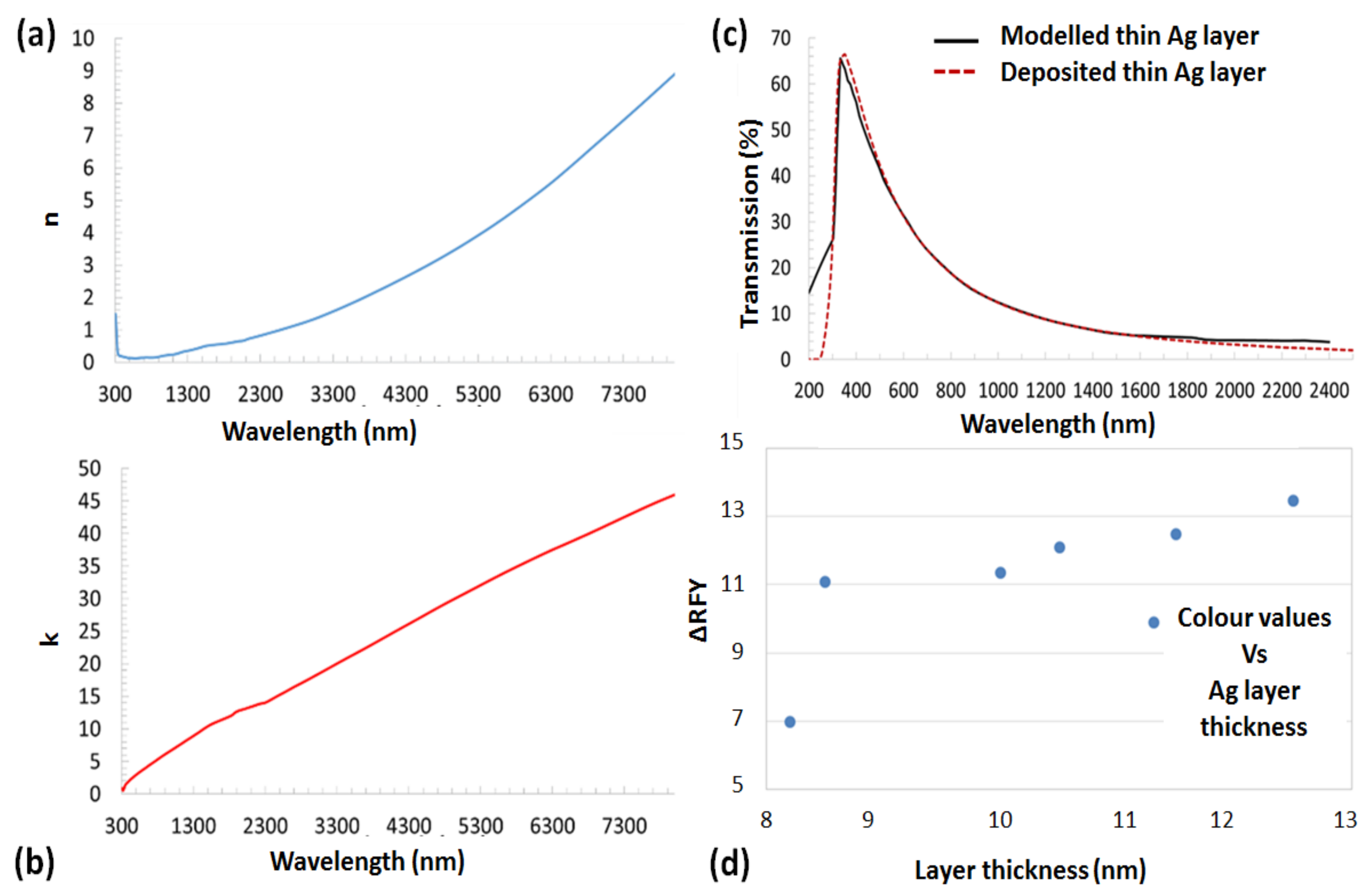
Despite the challenges of the deposition of ultra-thin Ag films with minimal surface roughness, homogeneous layer morphology, and perfect thickness control, silver is a well-known noble metal with the lowest optical losses throughout a very broad spectral range extending from the blue to the near-infrared wavelengths [32]. Another field in today’s fast-paced research and development environment is plasmonics nano-sensor development, which has lately seen a number of important breakthroughs [33,34,35,36,37,38]. Due to their great sensitivity to the refractive index change in dielectric media placed on top of ultra-thin plasmonics metal films, these surface plasmon resonance-based optical sensors have various commercial applications in oil and gas, biochemical, medical, and chemical sensing (Ag). Figure 2 (which is partially reproduced from Ref. [32]) presents the important parameters and optical characteristics of sputtered Ag thin layers.
The dispersion function of Ag layers’ optical constants (refractive index and absorption coefficient) is found to be patchy, partly owing to film thickness dependence and partly due to investigations being confined to a small wavelength range. We gathered all available information on the optical constants of Ag layers from all accessible sources throughout our coatings development work (conducted between 2011 and 2015, mainly unpublished so far) and discovered data inconsistencies in the 1000–2000 nm range. To acquire an acceptable quality of optical constant data between 300 and 7000 nm, we experimentally modeled and fitted numerous transmission spectra of deposited Ag films of varied thicknesses (12.5–40 nm). The revised dataset is shown in Figure 2a,b, in which our fitted data are combined with data from [39,40], resulting in close agreement between the modeled and observed transmission spectra for all film thicknesses. Figure 2c shows the fitted transmission spectrum of an as-deposited Ag layer of around 20 nm thickness obtained using OptiLayer modeling and spectrophotometry using this data set. We were able to establish that the thickness of our originally deposited layer was around 19 nm, which is correct to within 5%. Figure 2d shows the Ag layer thickness-dependent variation in color values; mainly, the lightness function (ΔRFY). In this work, we define the value of ΔRFY by subtracting the obtained value of Y (which is Yxy values as reported in CIE Chromaticity Coordinates) on the Ag layer from the Y value of clear glass substrate.

3.2. Features and Properties of RF Sputtered SiC Thin Films

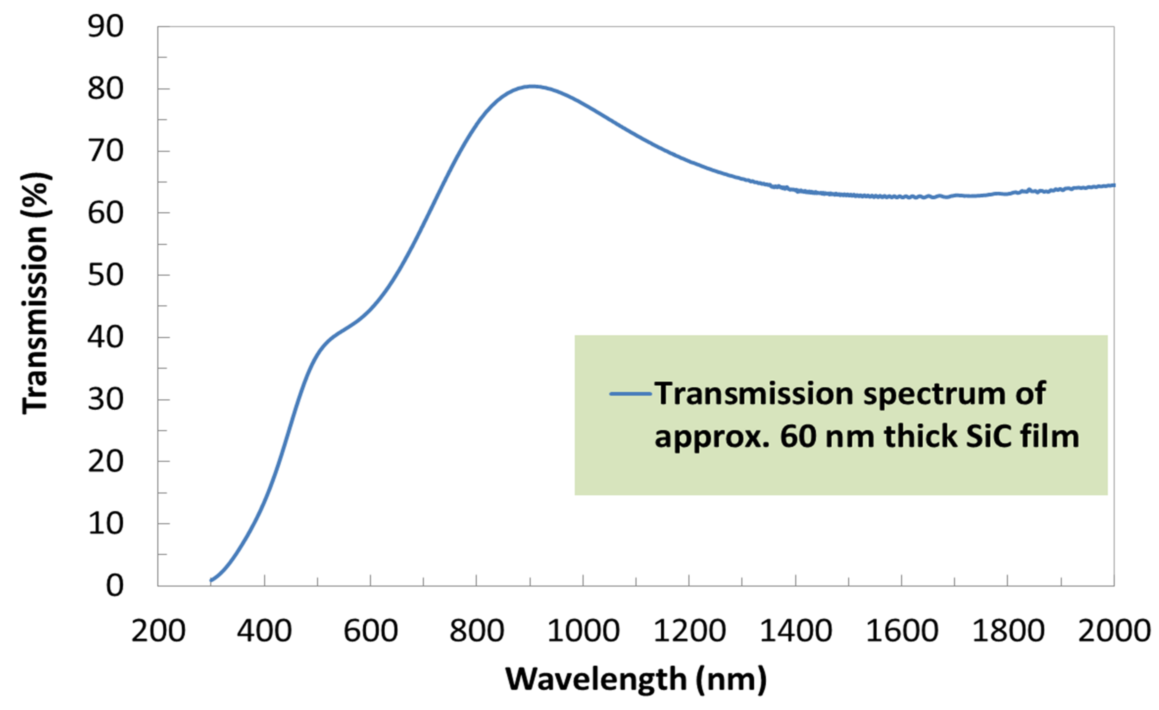
Amorphous SiC films were chosen because of their comparatively low growing temperature, which ensures greater compatibility with silicon-based technologies. However, in order to maximize the growing circumstances, high-quality films must be obtained [33]. We sputtered SiC thin films from a ceramic-type solid SiC sputtering target using the RF magnetron sputtering technique. The transmission spectrum of sputtered SiC film (as shown in Figure 3) confirms the semitransparent properties that can be varied depending on the film thickness.
It is well known that the refractive index of amorphous SiC strongly depends on film composition and film thickness. According to Aakash Mathur et al. [30], the refractive index of SiC thin films decreased from 2.97 to 2.77 with increasing film thickness, confirming that the performance of SiC in diverse applications may be improved by tuning of optical characteristics.

3.3. Properties of Ag+ SiC Nanocomposite Layers on Optical Glass Substrates

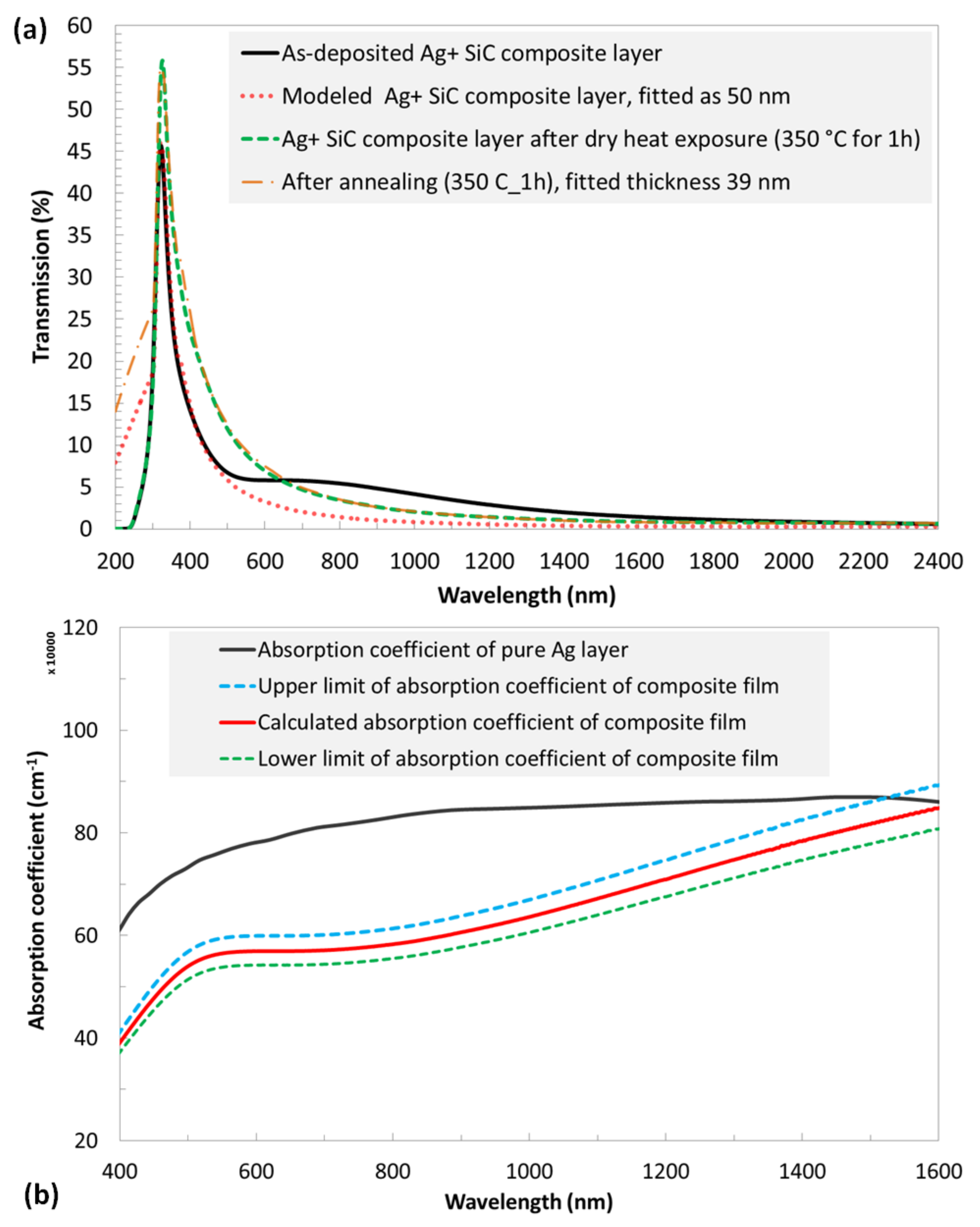
Figure 4 shows the optical characterization results obtained. It can be seen that the measured transmission spectrum was fitted with the modeled transmission spectrum, to re-confirm the actual layer thickness. It was found that the transmission spectrum of the as-deposited composite films matched that of a 50 nm modeled layer. However, after the heat treatment (trialed annealing runs between 200~450 °C for an hour), slight changes in the transmission spectra were observed (as can be seen in Figure 4a).
A small hump on the spectral response of the as-deposited composite layer was observed in comparison to that of the modeled layer; however, significant spectral shifts were observed in all of the high-temperature (above 300 °C) heat-treated films. The modeling of the nanocomposite layer transmission involved using a weighted average of the dielectric permittivities of the material components, using OptiLayer software. All of the heat-treated samples showed comparatively smoother transmission spectra, which might imply that the additional SiC compound transforms from the amorphous phase to the quasi-crystal stage, and this helps protect the pure-silver content from agglomeration or turning into nanoparticles. From the measured transmission spectrum of the as-deposited composite layer, we numerically evaluated the possible range of the absorption coefficient of the composite film, across a wide spectrum. Figure 4b shows the obtained wavelength-dependent absorption coefficient plotted within its possible upper and lower limits, compared to that of a pure silver layer. The upper and lower limits were evaluated by considering the maximum ±5% thickness error.
Figure 5 shows the morphological study results obtained on pure silver (Ag) and nanocomposite (Ag+ SiC) layers (subjected to dry heat exposure in the same conditions). It can be seen that the pure Ag layer turned into nanoparticles (the size and shape of the nanoparticle were relatively large, Figure 5a,b) while the composite layer showed resistance to turn into distinguishingly notable sizes of nanoparticles (Figure 5c,d). These results indicate that our composite material can withstand comparatively higher temperatures that are necessary for the production of high-standard commercial optical coatings. In the coating industries, the coating chamber temperature exceeds 180 °C where a pure metal layer can easily be turned into nanoparticles or can be oxidized due to the influence of the adjacent oxide layer of the coating structure.
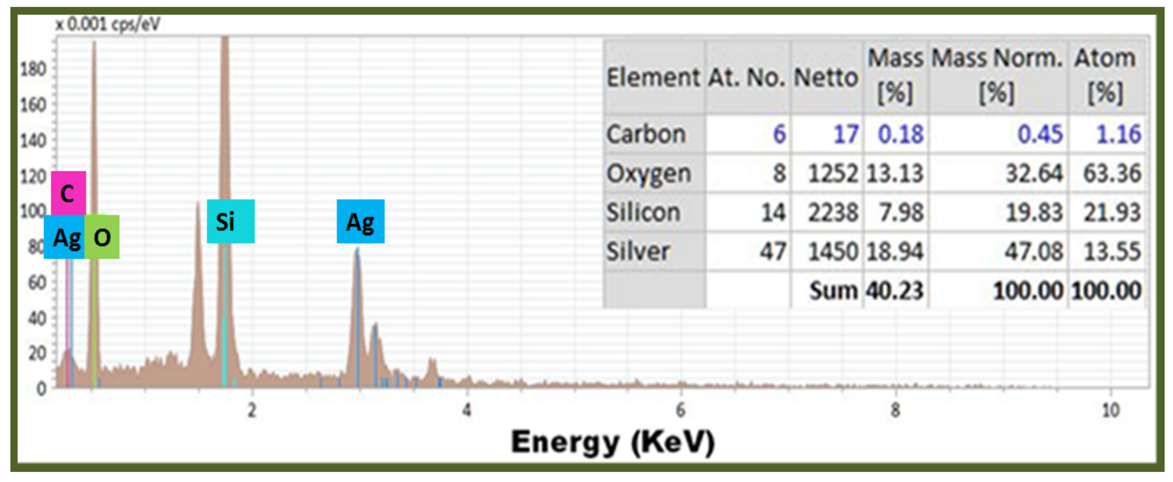
Figure 6 shows all the elemental constituents present in the Ag-based (SiC dilute) metallic composite thin films. It can be noticed that there is a large peak of Si observed which we believe is due to the presence of Si in the substrates (glass).

4. Conclusions

The development of metal-based nanocomposite material systems will potentially enable next-generation innovative optical components suitable for the development of cost-effective optical coatings on glass for various applications, including spectrally selective coatings and mirrors for thermal and heat regulation, thus enabling new directions in energy-efficient construction materials. This is due to the improved environmental exposure stability demonstrated in early experiments. We experimentally demonstrated that our new composite-type material is highly durable in high-temperature exposure (up to 350 °C) without having any significant change in its physical and optical properties. The wavelength-dependent absorption coefficients were found to be comparable to that of a pure silver layer. In addition, the ultra-fast sensing devices for various biomedical applications can also be designed and manufactured, based on using the metallic features and properties of this type of nanocomposite material.

Author Contributions

Conceptualization, M.N.-E.-A.; methodology, M.N.-E.-A., M.K.B. and M.V.; software, M.N.-E.-A. and M.V.; formal analysis, M.N.-E.-A., M.K.B., M.V. and N.D.; investigation, M.N.-E.-A. and M.K.B.; data curation, M.N.-E.-A., M.K.B., and M.V.; writing—original draft preparation, M.N.-E.-A.; writing—review and editing, M.N.-E.-A., M.K.B., M.V. and N.D.; visualization, M.N.-E.-A. and N.D. All authors have read and agreed to the published version of the manuscript.

Funding

This research received no external funding.

Institutional Review Board Statement

Not applicable.

Informed Consent Statement

Not applicable.

Data Availability Statement

Not applicable.

Conflicts of Interest

The authors declare no conflict of interest.

References

  1. Nur-E-Alam, M.; Lonsdale, W.; Vasiliev, M.; Alameh, K. Application-Specific Oxide-Based and Metal–Dielectric Thin-Film Materials Prepared by Radio Frequency Magnetron Sputtering. Materials 2019, 12, 3448. [Google Scholar] [CrossRef] [Green Version]
  2. Alias, R.; Mahmoodian, R.; Abd Shukor, M.H. Development and characterization of a multilayer silver/silver-tantalum oxide thin film coating on stainless steel for biomedical applications. Int. J. Adhes. Adhes. 2019, 92, 89–98. [Google Scholar] [CrossRef]
  3. Ochirkhuyag, N.; Matsuda, R.; Song, Z.; Nakamura, F.; Endo, T.; Ota, H. Liquid metal-based nanocomposite materials: Fabrication technology and applications. Nanoscale 2021, 13, 2113–2135. [Google Scholar] [CrossRef]
  4. Vannozzi, L.; Iacovacci, V.; Menciassi, A.; Ricotti, L. Nanocomposite thin films for triggerable drug delivery. Expert Opin. Drug Deliv. 2018, 15, 509–522. [Google Scholar] [CrossRef] [PubMed]
  5. Jin, W.; Maduraiveeran, G. Recent advances of porous transition metal-based nanomaterials for electrochemical energy conversion and storage applications. Mater. Today Energy 2019, 13, 64–84. [Google Scholar] [CrossRef]
  6. Lustig, W.P.; Mukherjee, S.; Rudd, N.D.; Desai, A.V.; Li, J.; Ghosh, S.K. Metal–organic frameworks: Functional luminescent and photonic materials for sensing applications. Chem. Soc. Rev. 2017, 46, 3242–3285. [Google Scholar] [CrossRef] [PubMed]
  7. Paladini, F.; Pollini, M.; Sannino, A.; Ambrosio, L. Metal-Based Antibacterial Substrates for Biomedical Applications. Biomacromolecules 2015, 16, 1873–1885. [Google Scholar] [CrossRef]
  8. Zhao, Y.; Lunt, R.R. Transparent Luminescent Solar Concentrators for Large-Area Solar Windows Enabled by Massive Stokes-Shift Nanocluster Phosphors. Adv. Energy Mater. 2013, 3, 1143–1148. [Google Scholar] [CrossRef]
  9. Meinardi, F.; Ehrenberg, S.; Dhamo, L.; Carulli, F.; Mauri, M.; Bruni, F.; Simonutti, R.; Kortshagen, U.; Brovelli, S. Highly efficient luminescent solar concentrators based on earth-abundant indirect-bandgap silicon quantum dots. Nat. Photonics 2017, 11, 177–185. [Google Scholar] [CrossRef]
  10. Merkx, E.P.J.; ten Kate, O.M.; van der Kolk, E. Rapid optimization of large-scale luminescent solar concentrators: Evaluation for adoption in the built environment. Opt. Express 2017, 25, A547. [Google Scholar] [CrossRef] [Green Version]
  11. Cocilovo, B.; Hashimura, A.; Tweet, D.J.; Voutsas, T.; Norwood, R.A. Highly transparent light-harvesting window film. Appl. Opt. 2015, 54, 8990. [Google Scholar] [CrossRef] [PubMed]
  12. Vasiliev, M.; Alghamedi, R.; Nur-E-Alam, M.; Alameh, K. Photonic microstructures for energy-generating clear glass and net-zero energy buildings. Sci. Rep. 2016, 6, 31831. [Google Scholar] [CrossRef]
  13. Dalapati, G.K.; Kushwaha, A.K.; Sharma, M.; Suresh, V.; Shannigrahi, S.; Zhuk, S.; Masudy-Panah, S. Transparent heat regulating (THR) materials and coatings for energy saving window applications: Impact of materials design, micro-structural, and interface quality on the THR performance. Prog. Mater. Sci. 2018, 95, 42–131. [Google Scholar] [CrossRef]
  14. Rezaei, S.D.; Shannigrahi, S.; Ramakrishna, S. A review of conventional, advanced, and smart glazing technologies and materials for improving indoor environment. Sol. Energy Mater. Sol. Cells 2017, 159, 26–51. [Google Scholar] [CrossRef]
  15. Yang, C.; Lunt, R.R. Limits of Visibly Transparent Luminescent Solar Concentrators. Adv. Opt. Mater. 2017, 5, 1600851. [Google Scholar] [CrossRef]
  16. Vasiliev, M.; Alameh, K.; Nur-E-Alam, M. Spectrally-Selective Energy-Harvesting Solar Windows for Public Infrastructure Applications. Appl. Sci. 2018, 8, 849. [Google Scholar] [CrossRef] [Green Version]
  17. Mohelnikova, J. Materials for reflective coatings of window glass applications. Constr. Build. Mater. 2009, 23, 1993–1998. [Google Scholar] [CrossRef]
  18. Vasiliev, M.; Nur-E-Alam, M.; Alameh, K. Highly Stable Thin-Film Multilayers For Thermal Regulation and Energy Savings in Smart Cities. In Proceedings of the 2019 IEEE 16th International Conference on Smart Cities: Improving Quality of Life Using ICT & IoT and AI (HONET-ICT), Charlotte, NC, USA, 6–9 October 2019; pp. 229–231. [Google Scholar]
  19. Wang, L.; Shen, Z.; Du, G.; Wang, P.; Wang, P. The thermal stability of silver-based high reflectance coatings. Thin Solid Film. 2016, 616, 122–125. [Google Scholar] [CrossRef]
  20. Bulíř, J. Preparation of nanostructured ultrathin silver layer. J. Nanophotonics 2011, 5, 051511. [Google Scholar] [CrossRef]
  21. Nur-E-Alam, M.; Rahman, M.M.; Basher, M.K.; Vasiliev, M.; Alameh, K. Optical and Chromaticity Properties of Metal-Dielectric Composite-Based Multilayer Thin-Film Structures Prepared by RF Magnetron Sputtering. Coatings 2020, 10, 251. [Google Scholar] [CrossRef] [Green Version]
  22. Tavsanoglu, T.; Zayim, E.O.; Agirseven, O.; Yildirim, S.; Yucel, O. Optical, electrical and microstructural properties of SiC thin films deposited by reactive dc magnetron sputtering. Thin Solid Film. 2019, 674, 1–6. [Google Scholar] [CrossRef]
  23. Todi, R.M.; Sundaram, K.B.; Warren, A.P.; Scammon, K. Investigation of oxygen annealing effects on RF sputter deposited SiC thin films. Solid State Electron. 2006, 50, 1189–1193. [Google Scholar] [CrossRef]
  24. Eichentopf, I.-M.; Böhm, G.; Arnold, T. Etching mechanisms during plasma jet machining of silicon carbide. Surf. Coat. Technol. 2011, 205, S430–S434. [Google Scholar] [CrossRef]
  25. Sha, Z.D.; Wu, X.M.; Zhuge, L.J. Structure and photoluminescence properties of SiC films synthesized by the RF-magnetron sputtering technique. Vacuum 2005, 79, 250–254. [Google Scholar] [CrossRef]
  26. Wang, M.; Diao, X.G.; Huang, A.P.; Chu, P.K.; Wu, Z. Influence of substrate bias on the composition of SiC thin films fabricated by PECVD and underlying mechanism. Surf. Coat. Technol. 2007, 201, 6777–6780. [Google Scholar] [CrossRef]
  27. Lei, Y.; Yu, Y.; Ren, C.; Zou, S.; Chen, D.; Wong, S.; Wilson, I. Compositional and structural studies of DC magnetron sputtered SiC films on Si(111). Thin Solid Film. 2000, 365, 53–57. [Google Scholar] [CrossRef]
  28. Lim, D.C.; Ahn, H.S.; Choi, D.J.; Wang, C.H.; Tomokage, H. The field emission properties of silicon carbide whiskers grown by CVD. Surf. Coat. Technol. 2003, 168, 37–42. [Google Scholar] [CrossRef]
  29. Lattemann, M.; Nold, E.; Ulrich, S.; Leiste, H.; Holleck, H. Investigation and characterisation of silicon nitride and silicon carbide thin films. Surf. Coat. Technol. 2003, 174–175, 365–369. [Google Scholar] [CrossRef]
  30. Mathur, A.; Pal, D.; Singh, A.; Singh, R.; Zollner, S.; Chattopadhyay, S. Dual ion beam grown silicon carbide thin films: Variation of refractive index and bandgap with film thickness. J. Vac. Sci. Technol. B 2019, 37, 041802. [Google Scholar] [CrossRef]
  31. Amorim, M.; Savio, R.; Massi, M.; Santiago, H. Applications of SiC-Based Thin Films in Electronic and MEMS Devices. In Physics and Technology of Silicon Carbide Devices; InTech: London, UK, 2012. [Google Scholar]
  32. Nur-E-Alam, M.; Vasiliev, M.; Alameh, K. Dielectric/metal/dielectric (DMD) multilayers: Growth and stability of ultra-thin metal layers for transparent heat regulation (THR). In Energy Saving Coating Materials; Elsevier: Amsterdam, The Netherlands, 2020; pp. 83–112. [Google Scholar]
  33. Nikolajsen, T.; Leosson, K.; Salakhutdinov, I.; Bozhevolnyi, S.I. Polymer-based surface-plasmon-polariton stripe waveguides at telecommunication wavelengths. Appl. Phys. Lett. 2003, 82, 668–670. [Google Scholar] [CrossRef]
  34. Chen, J.; Li, Z.; Yue, S.; Gong, Q. Hybrid long-range surface plasmon-polariton modes with tight field confinement guided by asymmetrical waveguides. Opt. Express 2009, 17, 23603. [Google Scholar] [CrossRef] [PubMed]
  35. Nagaraj; Krokhin, A.A. Long-range surface plasmons in dielectric-metal-dielectric structure with highly anisotropic substrates. Phys. Rev. B 2010, 81, 085426. [Google Scholar] [CrossRef] [Green Version]
  36. Marini, A.; Skryabin, D.V.; Malomed, B. Stable spatial plasmon solitons in a dielectric-metal-dielectric geometry with gain and loss. Opt. Express 2011, 19, 6616. [Google Scholar] [CrossRef]
  37. Yan, J.-Y.; Li, L.; Xiao, J. Ring-like solitons in plasmonic fiber waveguides composed of metal-dielectric multilayers. Opt. Express 2012, 20, 1945. [Google Scholar] [CrossRef] [PubMed] [Green Version]
  38. Carton, O.; Ghaymouni, J.; Lejeune, M.; Zeinert, A. Optical Characterization of Porous Sputtered Silver Thin Films. J. Spectrosc. 2013, 2013, 1–6. [Google Scholar] [CrossRef]
  39. Palik, E. Handbook of Optical Constants of Solids, 1st ed.; Elsevier: Amsterdam, The Netherlands, 1991; Available online: https://www.elsevier.com/books/handbook-of-optical-constants-of-solids/palik/978-0-08-055630-7 (accessed on 25 June 2021).
  40. GenIndex. Available online: http://www.luxpop.com/ (accessed on 25 June 2021).
Figure 1. Schematic diagram of the sputtering geometry used to prepare the composite thin-film layers.
Applsci 11 06746 g001
Figure 2. Extrapolated digitized optical constants dispersion data (a,b), and the optical (c) [32], and color (d) characterization results for thin sputtered Ag layers. The color values (measured using Minolta 508D) for different Ag thicknesses show the variation in ΔRFY versus Ag layer thickness, which reflects the importance of characterization for optimum film development.
Applsci 11 06746 g002
Figure 3. Optical transmission spectrum of an amorphous SiC layer prepared by using RF magnetron sputtering technique.
Applsci 11 06746 g003
Figure 4. Optical characterization results were obtained from Ag+ SiC thin-film nanocomposite layers (a) transmission spectra and (b) optical absorption coefficient.
Applsci 11 06746 g004
Figure 5. Morphological study of heat-treated pure-Ag and Ag + SiC (5 vol.%) composite layers. SEM images of Ag thin layer were obtained after annealing at 350 °C for 1 h (a,b), and Ag + SiC composite thin layer was imaged after exposure to the same temperature (350 °C for 1 h) (c,d). Surface imperfections in images (c,d) may be due to surface contamination, or slight precipitation.
Applsci 11 06746 g005
Figure 6. Obtained results of the elemental study of Ag + SiC (5 vol.%) composite layer.
Applsci 11 06746 g006
Table 1. Summary of the process parameters and conditions used to prepare composite layers on glass substrates.
Process ParametersValues and Comments
Sputtering target stoichiometryAg, and SiC
Target sourcingAJA International Inc. 809 Country Way North Scituate, Massachusetts, MA 02066, United States
and Zhongnuo Advanced Material Technology Co., Ltd., Beijing, China
Base pressure (Torr)4–5 × 10⁻⁶
Argon (Ar) pressure≈2 mTorr
RF power densities54–64 W for Ag target and 110–120 W for SiC target
Substrate stage temperature (°C)Room Temperature (21–23 °C)
Substrate stage rotation rate16–16.5 (rpm)
Target to substrate stage distance18 cm
Dry heat treatment200 ~ 450 °C for an hour
Publisher’s Note: MDPI stays neutral with regard to jurisdictional claims in published maps and institutional affiliations.