1. Introduction
In the field of artificial intelligence (AI), deep learning has been tremendously successful over recent years, reaching unprecedented milestones in various fields, such as image recognition, natural language processing, genome analysis, and autonomous driving [
1]. The use of graphics processing units (GPUs) as accelerators for computation required in deep neural networks (DNNs) was pivotal for their success. However, the computational power needed for training state-of-the-art AI-related applications has doubled every 3.5 months in the last few years [
2]. Based on this, the energy consumption for computation and data movement in GPU-enabled DNNs might soon pose a bottleneck. Photonic solutions are being investigated as a promising alternative for realizing energy-efficient DNNs, due to the inherent parallelism and the possibility of implementing neural network inference using passive optical elements.
Several photonic neural networks have been recently proposed [
3,
4], based either on bulk or integrated optics solutions. Reconfigurable photonic integrated circuits (PICs), are particularly suited due to their flexibility, compactness, and potential energy-efficiency. In this paper, we present two photonic integrated reconfigurable linear processors based on
interferometric elements [
5]. These devices are versatile, being exploited over the years for optical processing and filtering [
6], programmable true-time optical delay lines [
7], and quantum information processing [
8,
9]. They are also suited for realizing the linear operations (i.e., matrix–vector multiplications) required in each DNN layer. These analog operations are performed optically at high speed and in parallel, i.e., for all neurons in a DNN layer at once. Physical impairments affect the obtained results, reducing the effective number of bits (ENOB) that can be extracted when they are digitally converted in the electrical domain for storage and subsequent use. However, recent results exploiting reduced-precision numerical formats for neural network computation strongly motivate the use of a few-bit resolution. This opens up the possibility to exploit analog hardware to accelerate DNN with tolerable or even negligible accuracy losses in the DNN model prediction [
10,
11,
12,
13]. While the photonic processors presented in this paper can be exploited to implement the linear operations is DNNs, the nonlinear activation function can be emulated in software [
14] or implemented within the analog-to-digital converter without impacting the power consumption of the electronic front-end [
15].
In the paper, we present and compare two linear optical processors realized in different passive photonics integration platforms: silicon-on-insulator [
16] and silicon nitride [
17]. Furthermore, we discuss the scalability of this kind of linear processor and its suitability for accelerating state-of-the-art AI models for computer vision. The remainder of this paper is structured as follows: in
Section 2, we review the current research in the field of reduced-precision neural networks to provide the background and motivation for implementing neural network operations in the analog domain with limited resolution. In
Section 3, we present the fabricated reconfigurable linear optical processors. In
Section 4, we report the experimental results on the two devices, while in
Section 5, we discuss the impact of impairments on bit resolution and expressivity and application scenarios.
Section 6 concludes the paper.
2. Background on Low-Precision Neural Networks
In the last decade, a lot of research efforts on DNNs has been devoted to reducing the resources required to exploit neural networks with limited memory, storage or computing power (such as smartphones or network edge devices), as demonstrated by the success of TensorFlow Lite, the low-precision counterpart of the Google TensorFlow library. Two research lines emerged, the first one focusing on the inference phase only, leading to reduced-precision representation for the neural network parameters, and the second one aimed at speeding up the training phase using low-precision numerical formats for the gradients. The outcome of these research activities are of paramount importance for the implementation of analog photonic neural networks, as discussed in the following.
Concerning low-precision numerical formats currently used in electronic DNNs, three main approaches can be distinguished:
Use of low-precision floating-point formats;
Use of low-precision fixed-point real numbers or integer numbers;
Use of binary/ternary formats.
These alternative representations can be limited to the weights or to the weights and activations, or include all involved quantities (weights, activations, and gradients). When following the first approach (i.e., low-precision floats), research and development efforts are converging toward a 16-bit floating point representation instead of the classical 32-bit one [
18]. The main challenge concerns the lack of standardization; in particular, the number of bits reserved for the exponent part has not been defined yet. Although six bits can be used, there are reasons to use five (as recommended by IBM in its DLFloat format [
19]) or eight (as suggested by Google [
20]). This gap in the standard might be resolved soon, as there is a strong push from the machine learning community for suitable arithmetic formats. Another shortcoming of this approach is the lack of hardware support: most CPUs support 32- and 64-bit floats, but not 16- or 8-bit floats. Moreover, there are proposals to use a completely different representation for real numbers, such as the posit format introduced in 2017 [
21]. Although the posit format is promising for low-precision DNNs [
22,
23,
24], the lack of hardware support on CPUs still limits a large-scale adoption.
The second approach (i.e., low-precision fixed-point numbers or integer numbers) is popular since it allows DNNs to run even on entry-level CPUs micro-controllers not equipped with a floating point unit, since just an arithmetic logic unit is needed. On the one hand, fixed-point representations for real numbers are widely used (especially in financial applications and to improve the graphics in video games) even though C++ does not yet have a standard library supporting them. DNN implementations using low-precision fixed points for the both the weights and the activations are appearing [
25]. Recently, a few papers discussed the specific issues of training DNNs with a fixed-point representation [
26]. On the other hand, low-precision integer numbers are very interesting for time-sensitive applications, because operations between integer numbers have predictable computing times.
The third approach takes the use of low-precision integer numbers in DNNs to the extreme, using ternary or even binary weights. Remarkable results have been obtained: DNNs with ternary weights (i.e., −1, 0 and 1) have been demonstrated to achieve the same classification accuracy as DNNs using float32 weights [
27]. DNNs with binary weights have been also devised, again with little or no degradation in the classification accuracy [
28]. These results were confirmed on the very challenging ImageNet dataset, considered as the most demanding open-source dataset for visual object recognition, with more than 20,000 different object categories [
29]. The use of models with precision down to INT2 (i.e., 2-bit integer) has been demonstrated with a more than tolerable accuracy loss [
30,
31]. As a result, NVIDIA has added the support down to binary numbers to its top-level GPUs to perform tensor operations [
32]. Quantization can be applied either during the training phase or after it, just to perform the inference. However, DNN training using these numerical formats is more difficult compared to the two previously presented solutions as the gradient descent cannot be exploited, requiring the implementation of ad hoc learning algorithms.
Fixed-Point Representation for Analog Photonic Engines
Although the third approach (i.e., extreme quantization) is really appealing, binary and ternary representations are too drastic for an optical implementation, since the utilized optical technologies typically allow one to resolve more than two or three levels; moreover, they increase the complexity of the training with ad hoc learning algorithms. Therefore, in this work, we exploit the second approach, i.e., low-precision fixed-point real numbers or integers. This representation is inherently used by analog processors, such as the reported linear optical processors. Indeed, although analog signals can theoretically assume a continuous set of values, the ability to distinguish between them is limited by noise and distortions; this results in a finite and equally spaced set of numerical values of the output signal that can be distinguished.
In this scenario, the DNN can be trained on a CPU using a fixed-point representation for its weights and activations (but not for the gradients), which can be then utilized in the photonic neural networks. This neural network will then perform the inference at a much faster rate and at a fraction of the power consumption compared to electronic solutions. The problem of training such a network directly in photonics [
3] is outside the scope of this work.
3. Reconfigurable Linear Optical Processors
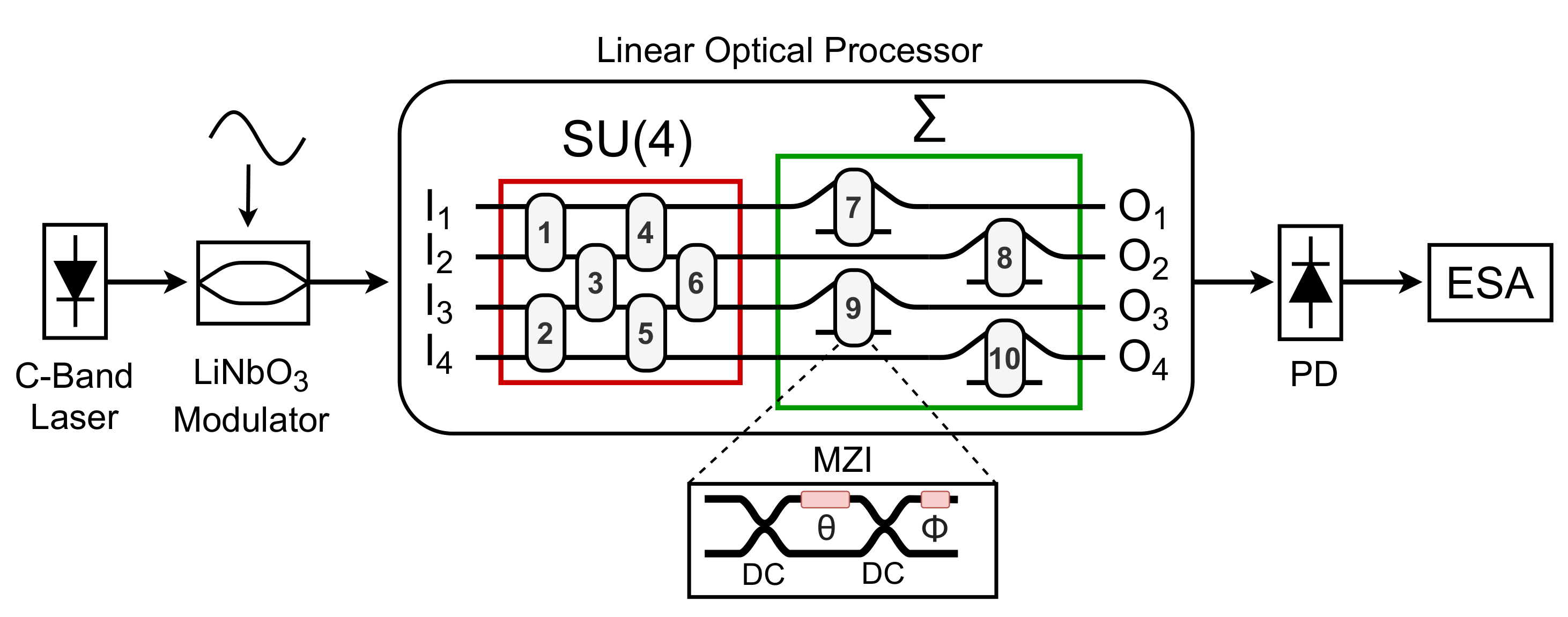
The basic element of a linear optical processor is a
reconfigurable Mach–Zehnder interferometer (MZI). It consists of two 3 dB couplers (realized by means of
multimode interferometers (MMI) or directional couplers) with a phase shifter on one of the internal arms (
) and another phase shifter at one of the outputs after the second coupler (
), as shown in the inset of
Figure 1. This MZI can implement any matrix in the special unitary group of degree two (i.e., SU(2)), composed of all complex square matrices whose conjugate transpose is equal to its inverse (unitary) and with a determinant equal to 1 (special unitary) [
33]. The MZI can be programmed by adjusting the two phase shifters,
and
.
By properly combining multiple MZIs, an
N-input
N-output structure can be created, which is capable of implementing any matrix in a special unitary group of degree
N (i.e., SU(
N)) [
34]. For instance, the device sketched in
Figure 1 is a
linear optical processor able to implement any SU(4), followed by a diagonal matrix multiplication section. The diagonal section (depicted as
in
Figure 1) makes it possible to extend the structure, by adding another SU(4), and thus carry out vector matrix multiplications with an arbitrary
matrix by exploiting a physical implementation of the singular value decomposition (SVD) theorem [
5]. These vector matrix multiplications constitute the linear operations performed in a neural network layers, followed by the application of the nonlinear activation function [
14].
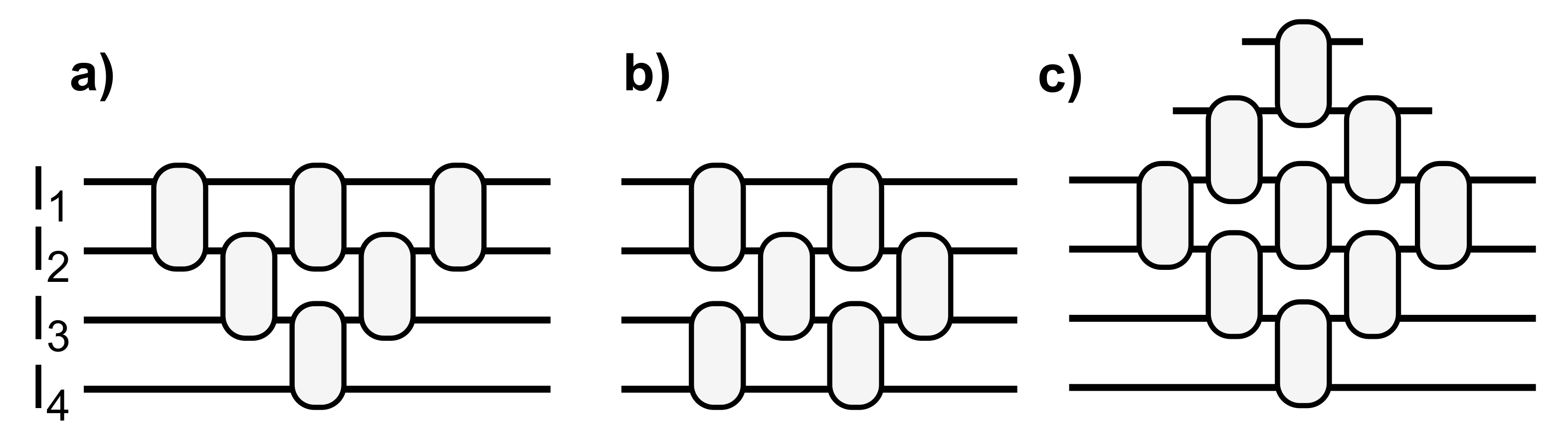
Several MZI arrangements, sketched in
Figure 2, can be chosen to implement such reconfigurable linear optical processors. MZIs can be organized in a triangular shape, i.e., a “Reck” architecture [
34], shown in
Figure 2a. With
N inputs, this architecture needs
MZIs to implement the
special unitary matrix, with a processor depth, defined as the maximum number of MZIs crossed on any input–output path, equal to
. Alternatively, in the “Clements” architecture, the same number of MZIs are arranged in a rectangular shape [
35], as exemplified in
Figure 2b. With the “Clements” architecture, optical path lengths are balanced and the processor depth is reduced to
N. Recently, a diamond architecture has been proposed as an extended version of the “Reck” topology [
36], obtained by adding
MZIs to the triangular one. This architecture, depicted in
Figure 2c, requires
MZIs, and has the same processor depth as the “Reck”,
.
Both the “Clements” and the diamond architectures are more robust to imperfections, noise, and loss with respect to the “Reck” one, translating into higher accuracies when used in neuromorphic applications [
35,
36]. However, the diamond mesh requires more MZIs, thus resulting in less power and footprint, and a more complex calibration. We also remark that, for all topologies, the number of phase shifters to be controlled scales quadratically with the size
N of the optical processor (i.e., with the number of input/ouput ports), which makes the handling of electrical I/O a nontrivial task.
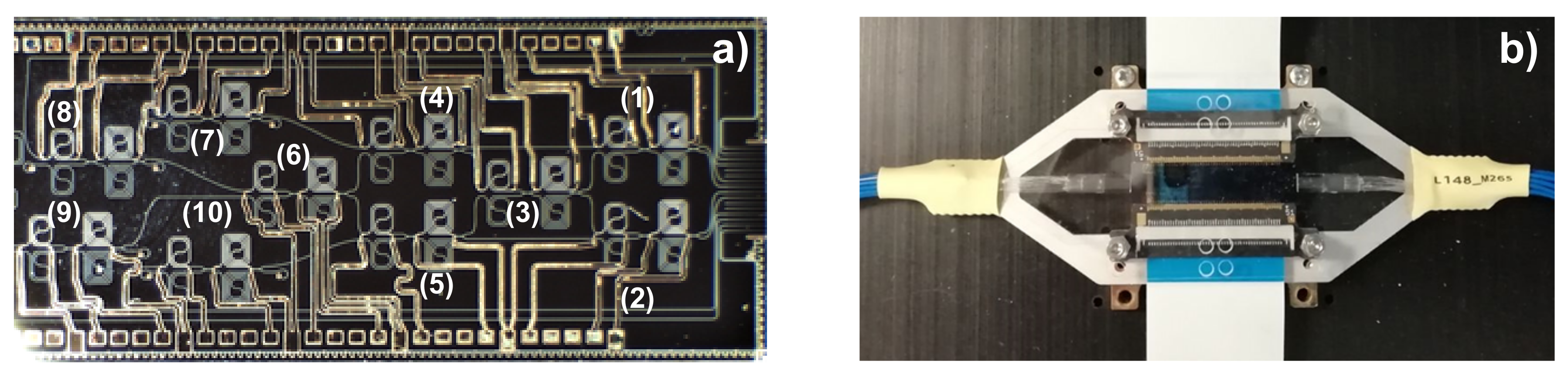
3.1. Silicon-on-Insulator Device
A first device with four optical inputs and four optical outputs has been realized in a silicon photonic e-beam MPW by ANT [
37]. The mask layout and the resulting chip are depicted in
Figure 3. The design objective was to achieve a small footprint, low loss, and broadband operation in the C-band to minimize the filtering effect, detrimental in large structures where many MZI are cascaded. MZIs are realized with MMI as 3 dB couplers and heater-based phase shifters. The device, implementing a “Reck” architecture followed by a diagonal matrix multiplication section, has 20 thermo-optic phase shifters connected to electrical pads on the PIC perimeter, 12 for the the
matrix and eight for the diagonal section. The size of the photonic integrated circuit is
mm
with the single MZI being 19
m wide and 519
m long, with 150
m heaters. Electrical pads on the lower and right hand sides are connected to each heater, while an array of eight grating couplers on the left hand side provides optical I/O. The overall chip footprint raises to
mm
due to grating couplers and the metal routes for the electrical I/O. The chip has been attached to a package and all electrical pads have been wirebonded. An eight-fiber array is positioned above the grating couplers to inject and extract optical signals to and from the chip.
3.2. Silicon Nitride Device
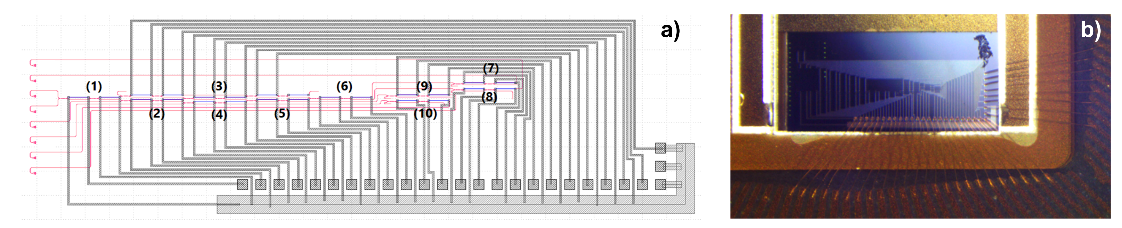
A second four-input four-output device, shown in
Figure 4, has been fabricated and packaged by LioniX International in a multi-project wafer run of the silicon nitride TriPleX platform based on asymmetric double-strip waveguides [
38]. It is composed of ten thermally tuned balanced MZI elements [
5], each of them realized using two 3 dB directional couplers and two phase shifters. The first six MZIs, arranged in a rectangular shape according to “Clements” architecture, implement the
unitary transformation matrix (i.e., SU(4)), while the last four MZIs implement the diagonal matrix multiplication section (i.e.,
) used to control the optical power at the four outputs. The four inputs and the four outputs of the linear optical processor are terminated at the chip edge with spot size converters that guarantee low-loss coupling to single-mode fibers.
MZIs are designed with relatively long low-loss phase shifters (8 mm for the inner shifter, 4 mm for the external one) in order to be driven with low currents (<20 mA). MZI internal and external arms have a spiral shape (radius ≥ 105
m) to reduce their footprint. Nonetheless, the overall circuit is larger compared to its silicon-on-insulator counterpart, having a size of
8 mm
, considering also the optical and electrical I/O. The single MZI element is 2.4 mm long and 1.64 mm wide. As depicted in
Figure 4b, the chip has been placed on a submount, which is wirebonded and pigtailed with two 16-fiber fiber arrays, one of which is used for the linear optical processor.
4. Experimental Characterization
This section reports the experimental results obtained with the two integrated reconfigurable linear optical processors: one device per platform was available for testing. A first step consisted of the characterization of all thermal phase shifters within MZI elements to find their actual phase-current relation, using the procedure described in [
5]. Then, the two PICs have been validated for photonic analog processing. To this aim, the impact of the realized devices on the bit resolution of input signals was evaluated through the effective number of bits (ENOB) reduction. The ENOB is a standard figure of merit for the resolution of analog signals, reflecting the number of bits necessary to represent those signals in the digital domain [
39]. This is particularly relevant in the context of reconfigurable linear optical processors as they emulate a single DNN layer; signals are then undergo electrical and analog-to-digital conversion for successive use in the emulation of a successive layer.
The ENOB can be derived from the signal to noise ratio (SNR) and the total harmonic distortion (THD) at the output of an analog device when a reference sinusoidal optical signal crosses the device under test. For this characterization, as reported in
Figure 1, a LiNbO
Mach–Zehnder modulator (MZM) has been used in its linear region to impress a 10 GHz sinusoidal signal to the amplitude of an incoming lightwave at 1550 nm. The spectrum of this reference signal has been acquired using a broadband photodiode (bandwidth 50 GHz) connected to an electrical spectrum analyzer (ESA, bandwidth 45 GHz). The spectrum has then been compared to the spectra obtained after crossing the two linear optical processors in order to evaluate their impact on the SNR and THD, and thus on the data resolution through the ENOB.
4.1. Silicon-on-Insulator Device
The heaters exhibited an average I
and P
(i.e., the current and the power needed to impress a
phase shift) of 14.2 mA and 55 mW, respectively, with 275
average resistance. Each MZI has a loss of approximately 0.7 dB and an average extinction ratio (ER) of 26.8 dB, both evaluated near 1550 nm.
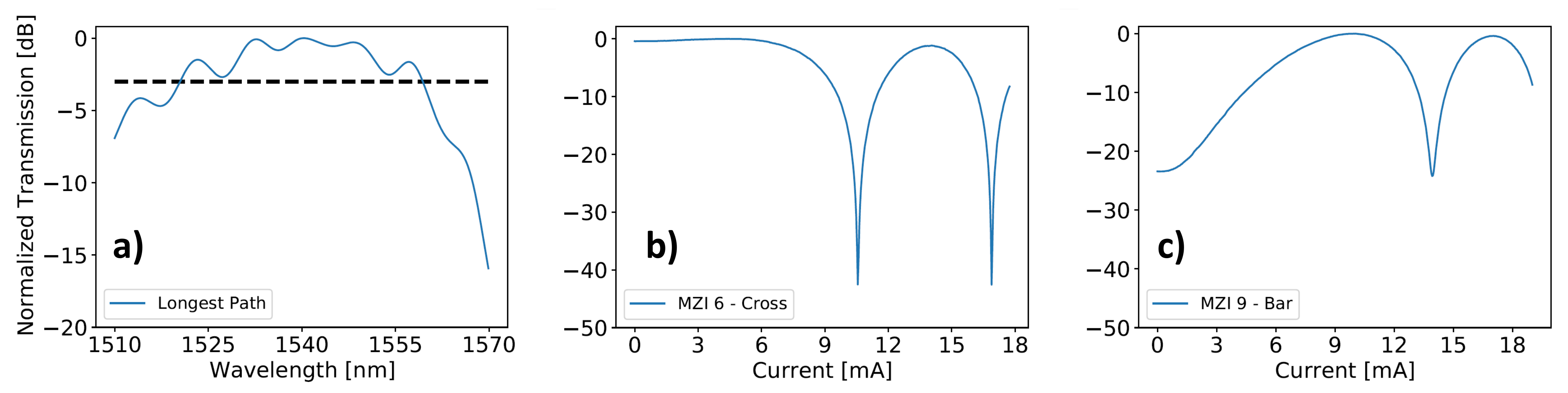
Figure 5a reports the normalized transmission along the longest path (from I
to O
in
Figure 3) accounting for the grating coupler (GC) spectral response: a 3 dB bandwidth of 35 nm can be appreciated, while the insertion loss (IL) is about 4.5 dB at 1550 nm along the same path crossing 6 MZIs, with an additional 6.5 dB loss per GC.
Figure 5b,c show the normalized transmission of MZI 6 in cross state and MZI 9 in bar state at 1550 nm, respectively, the best and the worst ones from an ER standpoint, with extinctions of 42.5 and 22.9 dB.
The impact on the bit resolution of input analog signals crossing the silicon-on-insulator linear optical processor has been then assessed.
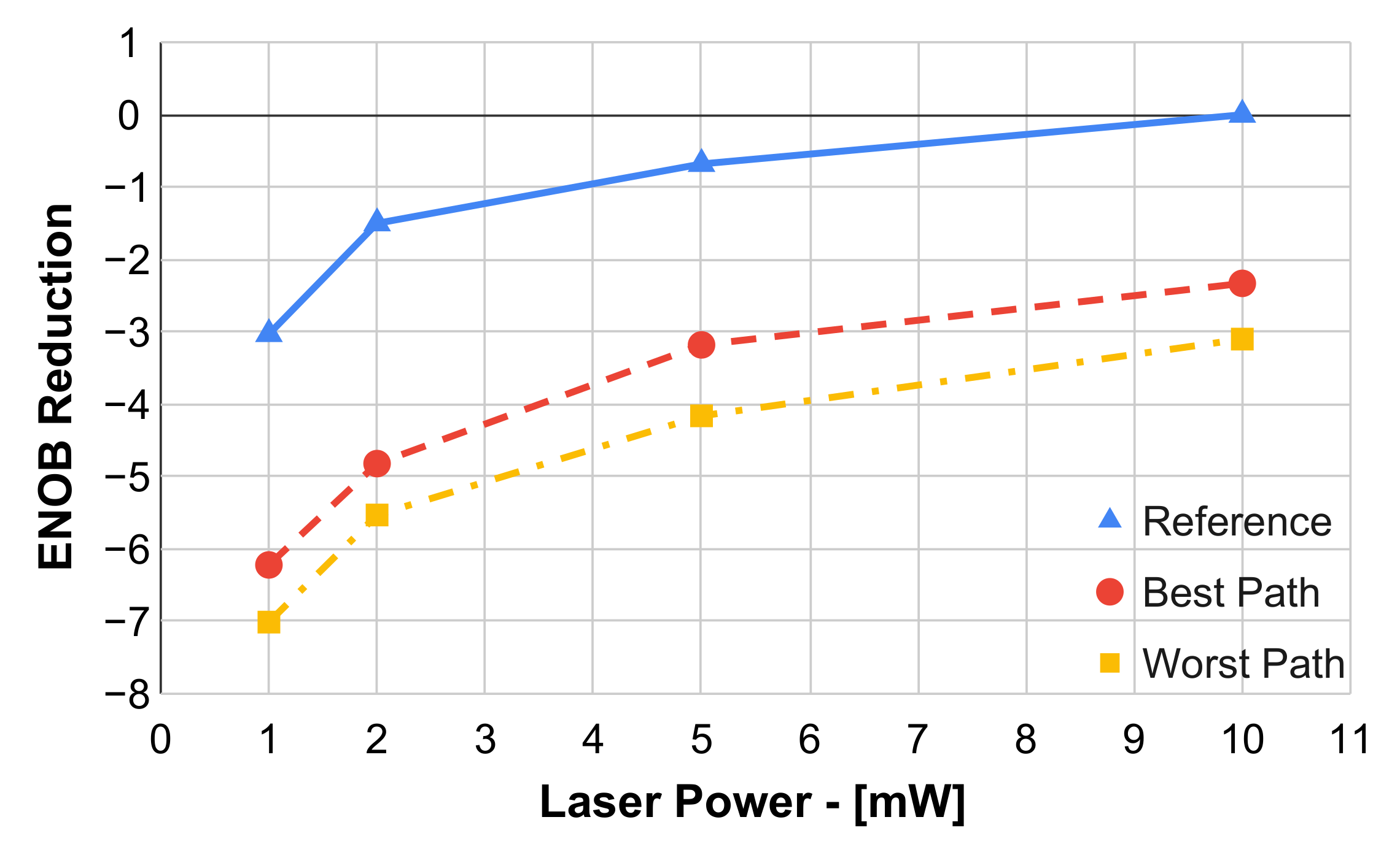
Figure 6 reports the ENOB reduction as a function of laser power with respect to the reference signal at the maximum power; the reference curve, as well as the the best and the worst device paths (i.e.,
and
, respectively) have been plotted. An ENOB degradation in the range 2.3–3.3 can be appreciated for the best path with respect to the reference, while the variation due to different paths is <1. Looking at the sources of ENOB reduction, they are mainly due to optical losses that directly degrade the SNR. Considering a 1 ENOB loss every 6.02 dB, the GCs alone are responsible for a loss more than two equivalent bits due to significant coupling losses. On the other hand, the analyzed spectra exhibited negligible distortions with a THD degradation < 1 dB.
4.2. Silicon Nitride Device
The internal shifters on the fabricated silicon nitride device showed an average I
of 10.2 mA with an average resistance of 2.8 k
, while the external phase shifters had 1.4 k
of resistance and an average I
of 14.5 mA; all were evaluated for operation at 1550 nm. The average P
resulted to be 296 mW. MZIs have an average loss of 1.5 dB and an average ER of 12.8 dB. After a careful analysis it has been found that both the excess loss and the relatively limited ER are mainly due to the directional couplers, which showed excess losses and unbalancing from the nominal 50/50 splitting ratio. The PIC exhibits a 3 dB bandwidth of about 40 nm, as reported in
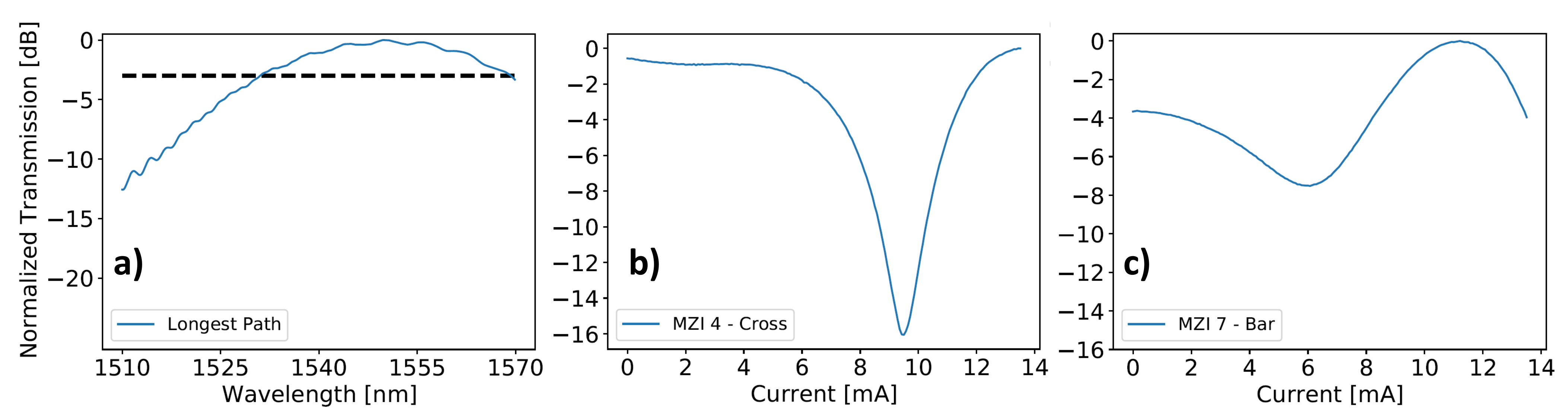
Figure 7a, showing the normalized transmission on the longest path as a function of the wavelength. In addition, the IL at 1550 nm along the same path is about 7.5 dB plus 3 dB from the two crossed spot size converters.
Figure 7b,c report the normalized transmission at 1550 nm of the best and the worst MZI from the ER standpoint (namely, MZI 4 in cross state and MZI 7 in bar state), with an extinction of 16.1 and 7.5 dB, respectively.
The impact of this silicon nitride processor on the bit resolution of analog signals has been then evaluated by acquiring and analyzing the spectra of the sinusoidal signal crossing the PIC with different configurations.
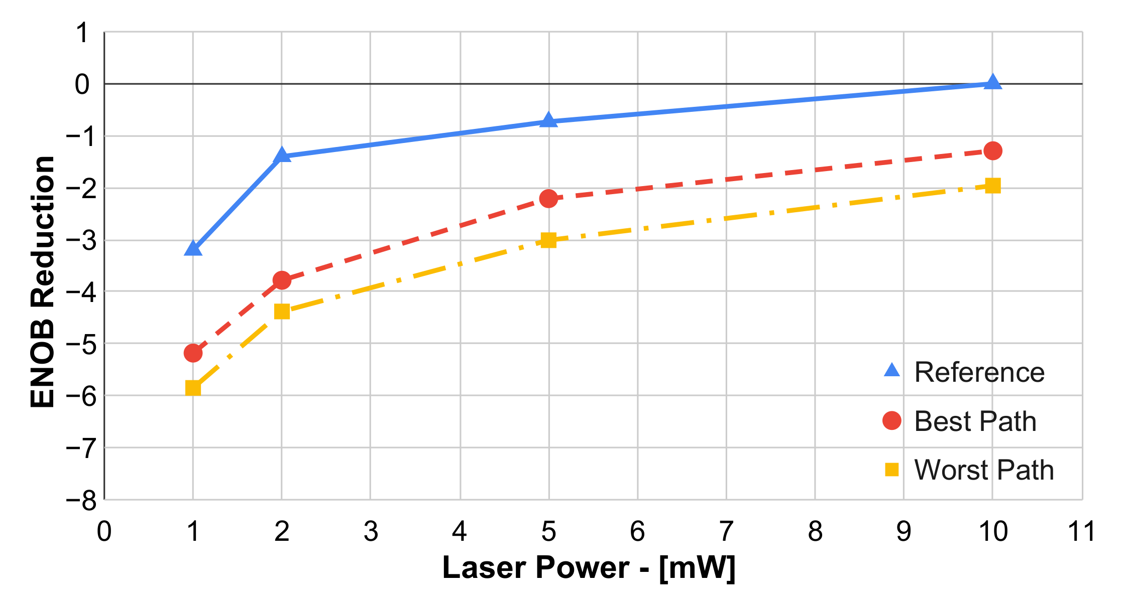
Figure 8 reports the bit resolution reduction as a function of the CW laser power normalized to the reference signal at the maximum laser power. The graph includes the reference curve, together with the ENOB reduction for the best and worst paths in the device, i.e.,
and
in
Figure 1, respectively. The ENOB reduction for the best path sits in the range 1.3 - 2.4 with respect to the reference curve, while the variation due to different paths is <1. As expected and similarly to the previous case, the PIC did not introduce spectral distortions, with a THD degradation <1 dB and the ENOB reduction mainly due to optical losses and related SNR decrease.
5. Discussion
The PIC performance as analog photonic processors can be evaluated by primarily considering two aspects: (i) the ability to optically process data without degrading the bit resolution of input signals, i.e., by keeping the ENOB unaltered; (ii) the ability to actually implement any SU(N), which is limited by the fabrication process inaccuracies. These aspects are detailed in the following, together with a discussion on the application of linear optical processors to computer vision tasks and a comparison of the realized photonic integrated devices.
5.1. Bit Resolution
Regarding the first point, the two solutions can be compared in terms of ENOB degradation. As reported in
Section 4.1 and
Section 4.2, no significant distortions nor noise are introduced by the PICs, being the optical loss the main source of ENOB degradation. This was expected since the devices are composed of passive elements and reconfigurable by means of thermal shifters. For this reason, the bit resolution comparison focuses on the IL determined by the MZI loss, the processor depth, and the optical I/O loss. The graphs in
Figure 6 and
Figure 8 show that the silicon nitride chip can perform the analog processing with higher resolution (about 1 ENOB) due to lower losses with respect to the silicon-on-insulator device.
Regarding the circuit topology, the “Clements” architecture is more convenient than the “Reck” architecture, given the same number of MZIs and the lower processor depth. The better scalability of “Clements” is apparent when devising larger size processors, since its processor depth is equal to the number of inputs
N, while the processor depth in the “Reck” architecture is almost double, growing as
, as discussed in
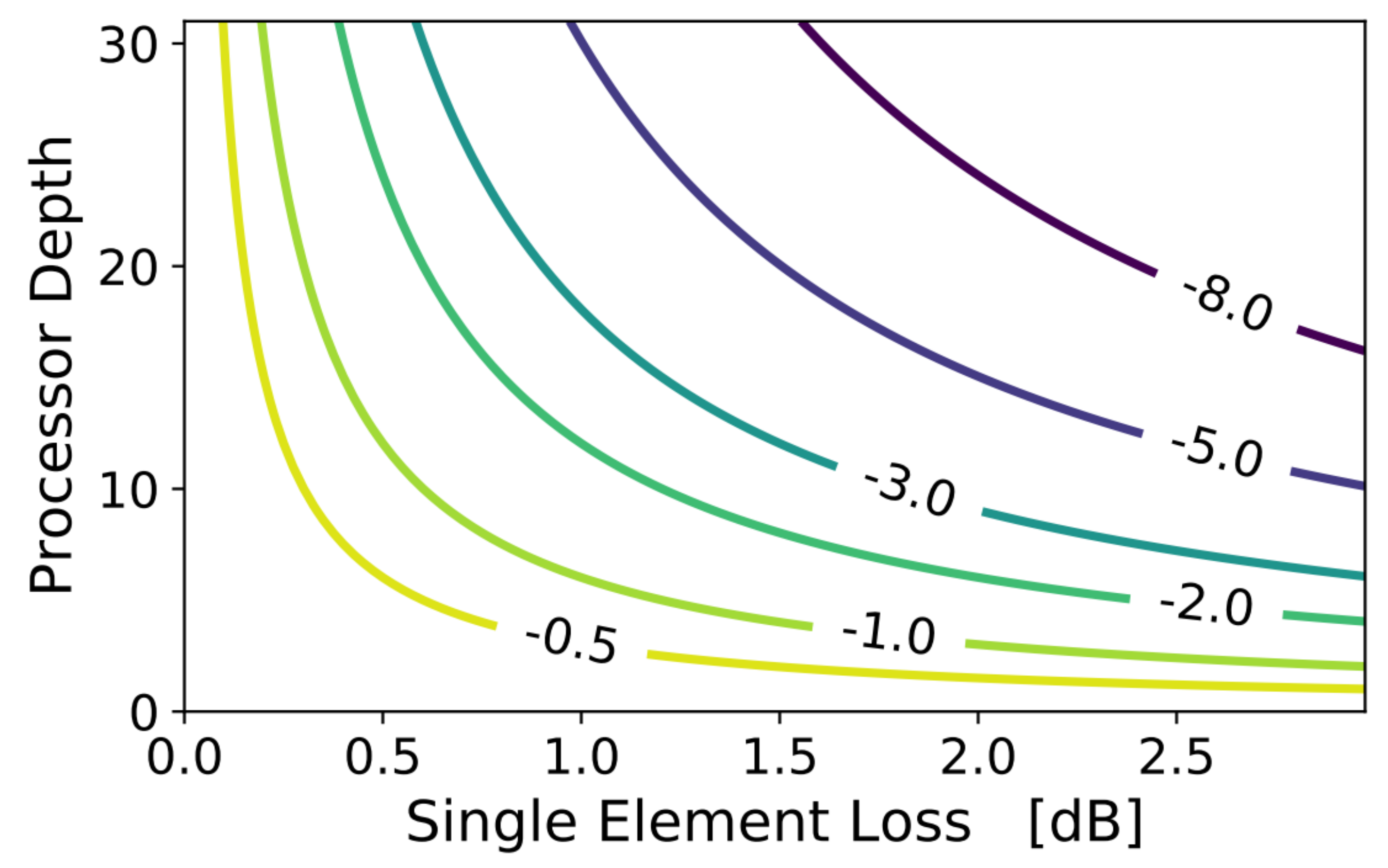
Section 3. Indeed, given the single element loss and neglecting optical I/O losses, the processor depth determines the ENOB reduction for all SNR-limited analog processors (not restricted to the case of PICs based on MZI meshes), as reported in
Figure 9. In this analysis that neglects optical I/O loss, the silicon-on-insulator chip, with an average MZI element loss of 0.7 dB, appears to be more scalable than the silicon nitride chip, with an average MZI element loss of 1.5 dB (more than double of the former). For instance, by restricting the ENOB reduction to be <2, this leads to a maximum silicon nitride processor depth of 8 with respect to 17 for the silicon-on-insulator processor.
5.2. Expressivity
Concerning the second aspect limiting the photonic processor performance, process variations should be considered that limit the PIC ability to implement any matrix in the SU(
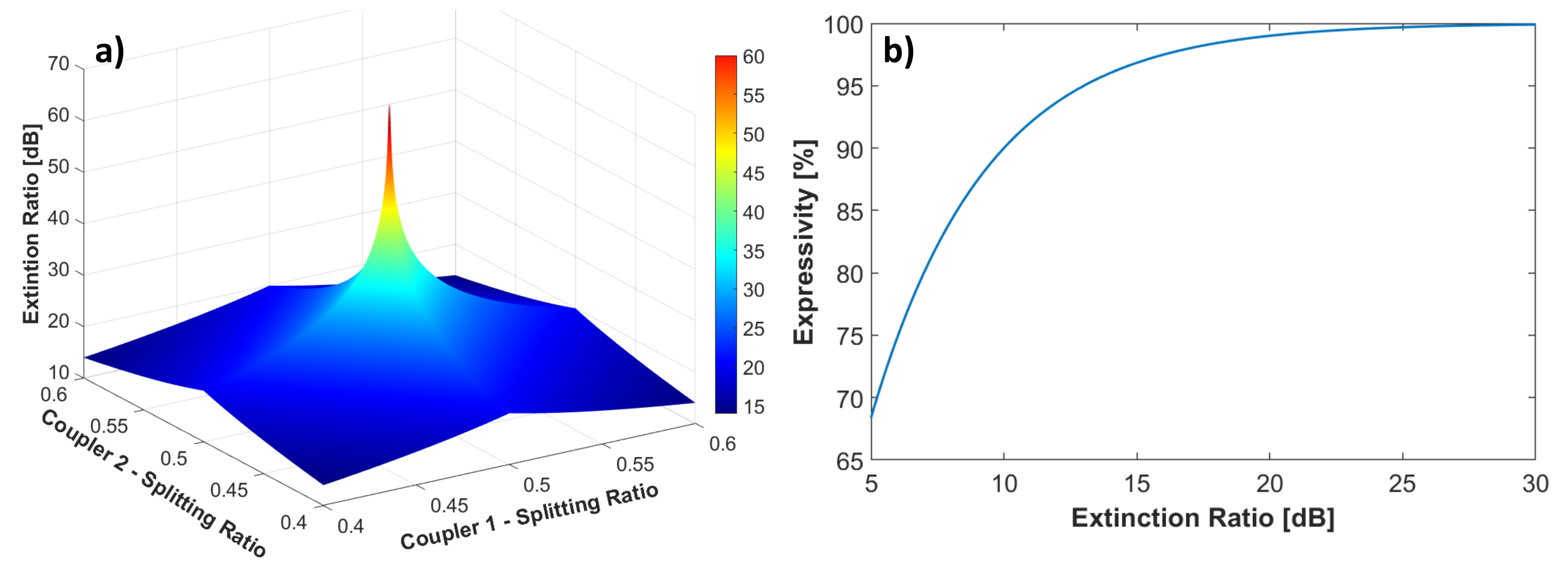
N) space, i.e., its expressivity. Fabrication inaccuracies primarily impact 3 dB couplers, causing an unbalance from the nominal 50/50 splitting ratio. The deviation from this nominal value decreases the MZI ER.
Figure 10a reports a 3D plot of the ER as a function of the splitting ratio of the two 3 dB couplers, within a 10% deviation from the ideal 0.5 splitting. The reported value is the minimum ER between the MZI bar and cross ports. The ER quickly decreases when deviating from the ideal splitting ratio, and reaches 25 dB when the two couplers have a splitting ratio of 0.47.
As discussed in
Section 3, an MZI should ideally implement any SU(2) matrix, which can be mapped on the surface of a Poincaré sphere [
40]. A finite ER prevents the single element from implementing any SU(2) matrix, thus reducing its expressivity, calculated as the fraction of reachable surface on the Poincaré sphere. To quantify this behaviour,
Figure 10b shows the MZI expressivity as a function of the ER. From this standpoint, the silicon-on-insulator chip outperforms the silicon nitride chip in terms of worst case MZI expressivity: since the worst ER is 22.9 dB, the former guarantees an MZI expressivity > 97%, while the latter, characterized by a modest ER of 7.5 dB in the worst case, reaches an MZI expressivity near 75%.
5.3. Linear Optical Processors for Computer Vision
Computer vision is probably the most relevant and wide application scenario in which deep learning has become a very successful and currently standard approach [
1]. Convolutional neural networks (CNNs) are the kind of DNNs used in computer vision, whose convolutional layers are composed of square filters with slow-changing parameters. Due to these peculiar features well matching the tuning speed of thermal phase shifters, CNN models are an interesting use case for assessing the presented photonic linear processors. Concerning computer vision tasks, ImageNet represents the most challenging image database for object recognition, composed of more than 14 million images and more than 2000 different object categories [
29]. Among the several CNN models proposed for the ImageNet challenge, Inception-ResNet-V2 represents a state-of-the-art deep CNN with super-human capabilities in object recognition [
41]. This CNN implements an advanced synthesis of two successful models: the inception module (from the Inception family) and the residual connection (from the ResNet family) [
41]. While the residual connection is a simple bypass of convolutional layers that highly improves the DNN ability to be properly trained [
42], the inception module is a modified convolutional layer that parallelizes multiple convolutional filters with different sizes to improve the CNN accuracy when detecting different size features. Convolutional filters are basically matrices used to process square portions of the image for extracting useful features: matrix values represent the network weights and are learnt during training. The advanced inception module of Inception-ResNet-V2 has been designed with the aim to simplify the convolutional filters, creating a deeper network with a lower number of learnable parameters. For this purpose, the larger
pixel-wide convolutional filters have been replaced by two cascaded
and
arrays. In the case of Inception-ResNet-V2, the replacement of
convolutional filters reduced the number of input per layer from 49 to 14, while the largest filters work on
pixels, corresponding to nine inputs. To perform the linear computation of Inception-ResNet-V2 convolutional layers in photonics, the maximum input size is thus 9. According to the singular value decomposition theorem outlined in
Section 3, two linear processors implementing SU(9) matrices plus a diagonal section are required. Exploiting the “Clements” architecture, these processors should have an overall depth of 19. With reference to the MZI element loss of the two PICs discussed above and the results in
Figure 9, a silicon photonic chip would exhibit an ENOB reduction of 2.2, while a silicon nitride chip would suffer a more significant ENOB reduction of 4.7.
Section 2 discusses the research on low-precision numerical representations that motivates the use of analog processors for neuromorphic computing. In this framework, the results on low-precision representations on the ImageNet dataset showed that numerical formats down to INT4 or INT2 can be used with limited accuracy losses [
30,
31]. Given these results, a final ENOB of 4 (equivalent to an INT4) would be a reasonable tradeoff between the classification accuracy and the implementation complexity. Given a typical input ENOB of about 6 [
15], the ENOB degradation due to analog processing should be < 2 to ensure the goal of a final ENOB ≥ 4. With reference to the results depicted in
Figure 9 the loss of a single element in the photonic processors with an overall depth of 19 should be below 0.63 dB, a value in line with demonstrated MZI-based photonic integrated switches [
43].
From a power efficiency standpoint, a 9-input layer processing input signals at 10 GHz implemented in a silicon-on-insulator device would dissipate 2.6 pJ/operation on average, while a silicon nitride device would have a energy consumption of 13.9 pJ/operation. These values are well in line with the ones outlined in the recent roadmaps on neuromorphic photonics [
44,
45].
5.4. Photonic Device Comparison
To conclude this section, we compare the realized devices in terms of several features relevant for photonic analog processors: (i) losses, that should be limited to ensure low ENOB degradations; (ii) footprint, to realize compact devices; (iii) phase shifter power consumption (estimated through P
), that should be low to realize energy-efficient photonic accelerators [
44,
45].
Table 1 reports an overview of the most important values found in the experimental characterization and measurements performed on the two reconfigurable linear optical processors in this work. For a proper comparison, the table lists also the values taken from other MZI-based reconfigurable chips, three in the silicon-on-insulator platform and one in the silicon nitride platform. Results include the scalability of the processors evaluated as the highest processor depth causing an ENOB reduction < 2, and the energy per operation on a nine-input layer. Expressivity, ENOB reduction, and scalability have been derived also for the architectures in the literature. Concerning chip-to-chip process variations, the reader is referred to [
46,
47].
The silicon-on-insulator chip, despite the rather high chip-to-fiber coupling losses due to the GC [
5], showed promising results due to the low loss and high ER of its basic MZI elements, the rather low P
of its thermal tuners, and the associated compactness. Nonetheless, using a different silicon-on-insulator process, insertion losses can drop down to 0.4 dB per element [
48] or even below 0.1 dB [
8]. This notable result presents the possibility to exploit SOI-based chips for large-scale parallel processing (processor depth >100) with reduced ENOB degradation. Spot size converters (SSCs) can mitigate the optical I/O losses down to 3.5 dB [
8], the ER can reach more than 60 dB [
8] with a consequent increase in expressivity, and thermal phase shifters can be more compact (<100
m) and energy-efficient with a halved [
5,
49] or almost twenty times lower [
48] P
.
The silicon nitride platform is renowned for very low propagation losses, as low as 1 dB/m [
50]. Indeed, the overall ENOB degradation was lower in the silicon nitride chip, mainly thanks to the lower chip-to-fiber coupling losses. However, in this work the realized photonic components, namely MZIs, were characterized by quite high losses and low ER. The DC IL can be reduced to < 0.1 dB, as reported in [
51], enabling the fabrication of a much deeper optical processor (up to 50 considering an ENOB loss < 2). The limited ER values are in line with the recent literature for this kind of processor [
52], but can be considerably improved according to the values reported in [
53], where an ER > 24 dB was found. The main reason for the limited ER can be traced back to the directional couplers, whose splitting ratio exhibits a standard deviation of 0.126 with respect to the nominal one, as reported in [
52]. Moreover, the rather high P
of its thermal phase shifters and the large PIC footprint, typical of this technology, highlighted some issues preventing the scalability of the design. Nonetheless, an interesting alternative to the thermal tuners could be pursued, regarding stress-optic modulators that exploit piezoelectric materials achieving an extremely low P
in the order of hundreds of nW [
54]. This perspective makes this technology still appealing for the development of very power-efficient analog photonic processors.
As outlined in this section, the main challenges in scaling up these optical processors are related to minimizing optical losses, footprint and deviation in the couplers from the ideal 50/50. Moreover, integrating the laser and the photodetectors would avoid optical I/O losses with large benefits in terms of signal bit resolution. Finally, even if all these problems were properly tackled, the handling of the electrical I/O would remain challenging as it scales quadratically in respect to the number of inputs.
6. Conclusions
In this paper we have reported the comparison of two reconfigurable linear optical processors based on thermally tunable MZI meshes. The PICs have been realized in silicon-on-insulator and silicon nitride platforms, implementing, respectively, the Reck and the Clements architectures. The latter is more convenient as it is compact and has balanced optical paths and a reduced optical depth with the same number of MZI elements. These devices are suited to compute matrix–vector multiplications analogically in the photonic domain, and they have been evaluated as neuromorphic accelerators to extract feature maps in convolutional neural networks. The processors do not introduce significant distortions nor noise. The bit resolution of processed signals is degraded due to optical losses, which ultimately limit their scaling. The silicon-on-insulator chip is characterized by a bit resolution reduction in the range of 2.3–3.3 for the best path, while for the silicon nitride chip the loss was found in the range of 1.3–2.4. In both cases, the reduction spread among all paths was <1. While this silicon nitride chip performs better compared the silicon-on-insulator one, the latter appears to be more suited to implement larger scale processors due to lower MZI element losses. Moreover, the impairments due to process tolerances result in a smaller ER of silicon nitride MZI elements, which limits their expressivity, i.e., the ability to actually implement any linear transformation. Finally, the silicon-on-insulator chip outperforms the silicon nitride one in terms of footprint and power efficiency.


 ,
, 


