Article

Independent Double-Boost Interleaved Converter with Three-Level Output

by
Vasile Mihai Suciu
,
Sorin Ionut Salcu
,
Alexandru Madalin Pacuraru
,
Lucian Nicolae Pintilie
,
Norbert Csaba Szekely
and
Petre Dorel Teodosescu
*
Department of Electrical Machines and Drives, Technical University of Cluj-Napoca, 400489 Cluj-Napoca, Romania
*
Author to whom correspondence should be addressed.
Appl. Sci. 2021, 11(13), 5993; https://doi.org/10.3390/app11135993
Submission received: 31 May 2021 / Revised: 22 June 2021 / Accepted: 23 June 2021 / Published: 28 June 2021
(This article belongs to the Special Issue Novel Power Electronics Technologies in Power Systems)

Abstract

:
This paper introduces a novel converter topology based on an independent controlled double-boost configuration. The structure was achieved by combining two independent classic boost converters connected in parallel at the input and in series at the output. Through proper control of the two boost converters, an interleaved topology was obtained, which presents a low ripple for the input current. Being connected in series at the output, a three-level structure was attained with twice the voltage gain of classic boost and interleaved topologies. A significant feature of the proposed converter is the possibility of independent operation of the two integrated boost converters, in both symmetrical and asymmetrical modes. This feature may be particularly useful in voltage balancing or interconnection with bipolar DC grids/applications. The operation principle, simulations, mathematical analysis, and laboratory prototype experimental results are presented.

1. Introduction

The need for high-gain boost topology converters with a low ripple of the input current can be justified in various applications, such as bidirectional chargers for electric vehicles in smart homes [1], development of energy storage for renewable power systems [2,3,4], and DC microgrid and mobility-related concepts [5,6,7,8]. The present work focuses on the power conversion stage of low voltage DC renewable sources, such as photovoltaic panels with power optimizers and/or micro-inverter applications in AC or DC distribution microgrids [9].
The classic interleaved boost converter is recognized for its high efficiency and low ripple input current. On the other hand, this type of converter exhibits a limited voltage gain. High-gain interleaved DC–DC voltage converters in transformerless structures have been explored in various studies [10,11,12,13]. A floating, high-gain voltage interleaved converter widely employed in research studies was analyzed in [14,15]. This structure is based on the principle of the intercalated operation of two classic boost converters. However, the output circuit for this application does not have purely capacitive filtering, thus it requires a more complex scheme for the output voltage control. Numerous studies commonly use the three-level boost converter [16], but since the input source and inductor currents are the same, there is no interleaved characteristic, and the voltage gain is limited. The same limitations were found in the research of [17], where a three-level DC–DC boost converter with dual output was presented. An interleaved step-up DC–DC converter topology composed of two boost converters was introduced in [18]. During operation, the converter stages are indirectly connected in a series, which ensures a high voltage gain of the output. Since the output consists of two series capacitors, a three-level output is achieved. The individual voltage drop across each capacitor is balanced according to the operating state of the converter, but a fully independent control is not achieved for this approach, and the efficiency at a low input voltage is limited. The same limitation regarding the independent voltage balancing of the output capacitors was found in [19].
High voltage gain non-isolated converters without coupled inductors exhibit a simpler structure, being more suited for low power level applications [20,21,22,23,24,25,26,27,28,29,30,31]. In Ref. [20], high conversion gain and efficiency were achieved using an interleaved topology. To acquire high voltage gain with low voltage stress across the semiconductor devices, [21] proposed the usage of an active–passive inductor cell configuration for a step-up DC–DC converter, and [22] showed that the implementation of a switched capacitor topology allowed a wide voltage gain range. In Refs. [23,24,25,26], multistage diode–capacitor (MSDC) networks were implemented. Similarly, in Ref. [27], a switched inductor and switched capacitor multilevel topology was involved, with the output voltage distributed among multiple levels of output capacitors, subsequently reducing the voltage stress on the components. Using two duty ratios to operate the switched states of the converter, Ref. [28] attained high voltage gain without using extreme values of these duty ratios, thus the voltage conversion proved to be more efficient. In addition, in Refs. [29,30,31], the converter topologies employed an interleaved design, with the inductors switched in a parallel and series configuration during the charging and discharging states. Despite the high voltage gain, in all the variants mentioned above, there was high voltage stress across the power semiconductors. All these converter topologies have good gain and efficiency, and some also have interleaved properties, but none have a three-level output with fully controlled voltage operation.
The present work introduces a novel interleaved converter topology that integrates two classic boost converters working independently, in parallel at the input and in series at the output. The circuit has high voltage gain capabilities, and in comparison with the work in [14,15], it exhibits pure capacitive filtering at the output, which enables a classical PI voltage control method to be used. Additionally, with three voltage level characteristics reached at the output in conjunction with the asymmetrical/independent operation of the integrated boost structures, the proposed converter topology could also be used in voltage balancing or interconnection with bipolar DC grids/applications [32]. Another major contribution of the present work is the unique integration of a multitude of useful features, such as interleaved, high-gain, good efficiency, low voltage stress, three-level output with symmetric/asymmetric operation, and stable control method, into a single electronic conversion solution.
Apart from the introduction, the paper is organized in the following structure. In Section 2, a detailed representation of the proposed topology and switching states is presented. Furthermore, an analysis of the converter in both the continuous conduction mode and discontinuous conduction mode is discussed in detail. Section 3 presents a study of the converter’s behavior, performed by software simulation and practical measurements on a laboratory model. In addition, the main features of the proposed topology in comparison with similar approaches are emphasized in this section. The conclusions and further work are presented in Section 4.

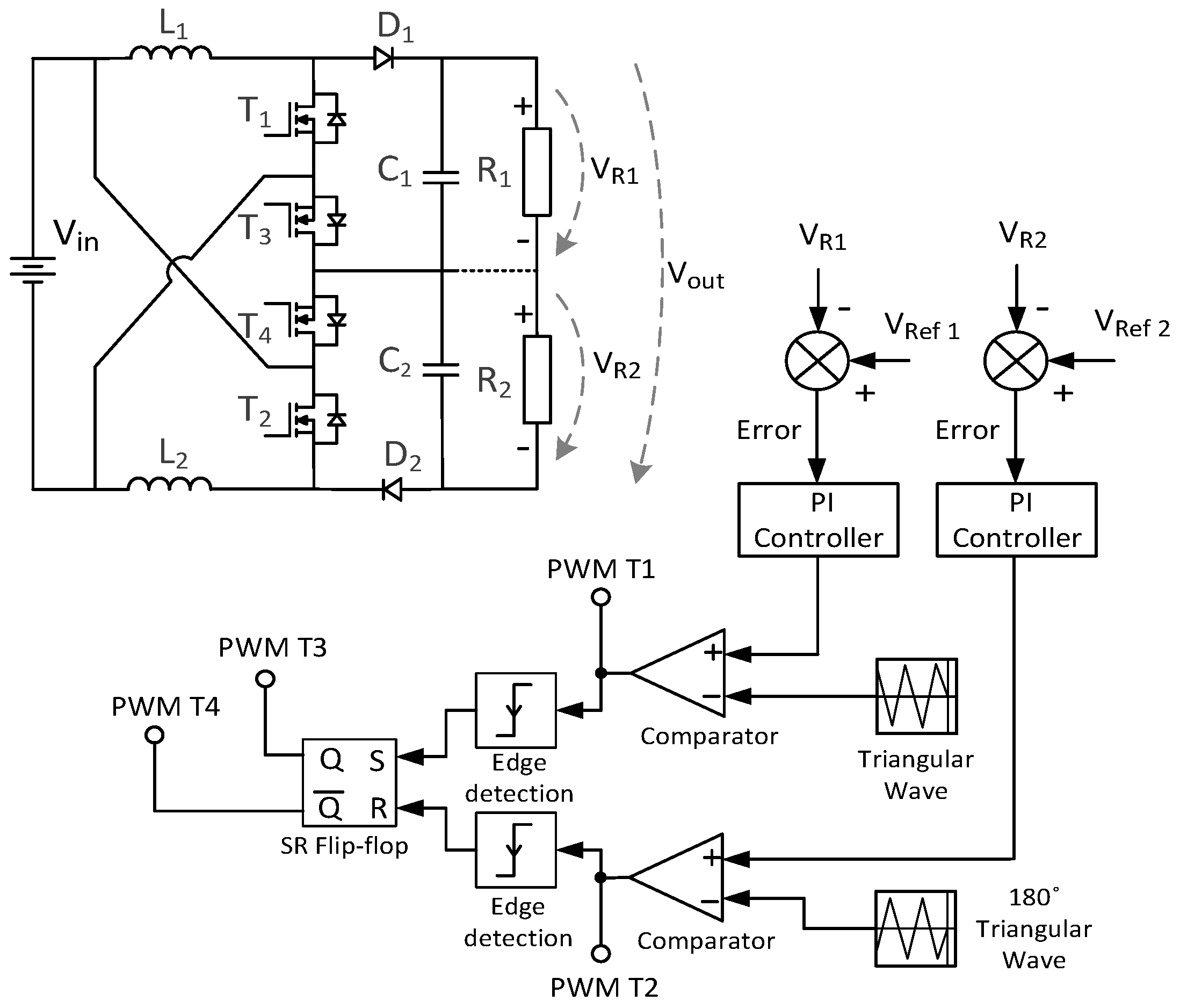
2. Converter Topology Analysis

2.1. Converter Topology, Switching States, and Presumptive Waveforms

The proposed converter topology, named an independent double-boost interleaved converter and henceforth referred to as IDBIC, is based on a patent application [33] developed especially for PV/wind energy harvesting and battery energy conversion systems. The basic converter topology is represented in Figure 1, while the main operating stages of the converter are presented in Figure 2, in which nine independent switching states (S1–S9) are underlined.
The characteristic waveforms during operation are introduced in Figure 3, in which the continuous conduction mode (CCM) and discontinuous conduction mode (DCM) operations are exemplified in conjunction with the S1–S9 switching states. These four presumptive switching patterns are mainly triggered by the duty cycle values of the T1 and T2 transistor command signals. In view of this, for a duty cycle smaller than 0.5, the inductor currents have steeper falling slopes during the S2 and S3 switching stages. For a duty cycle larger than 0.5, inductor current waveforms and behavior similar to the regular boost interleaved converter can be observed.
As documented in these switching stages and presumptive functioning patterns, the two integrated boost converters work independently from each other, with the inputs connected in parallel and the outputs in series. From this observation, one of the key characteristics of the proposed double-boost converter is defined.

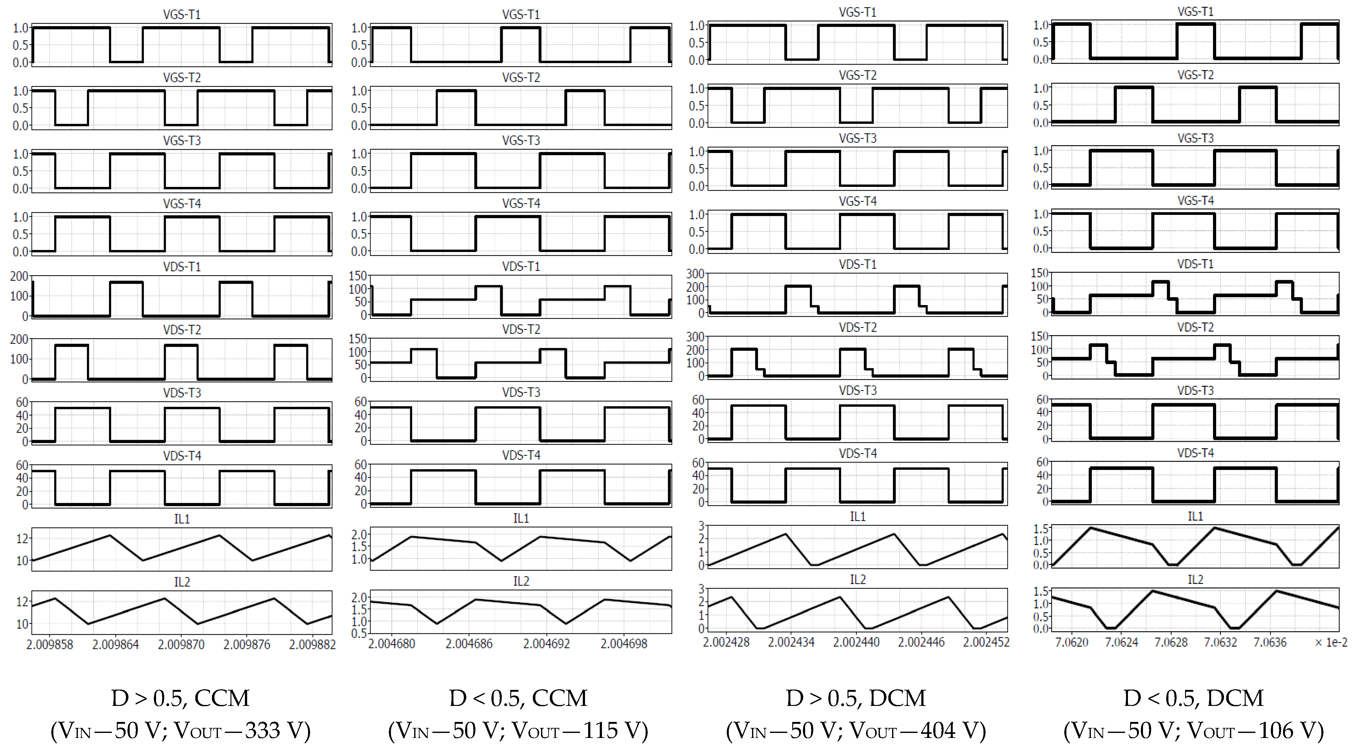
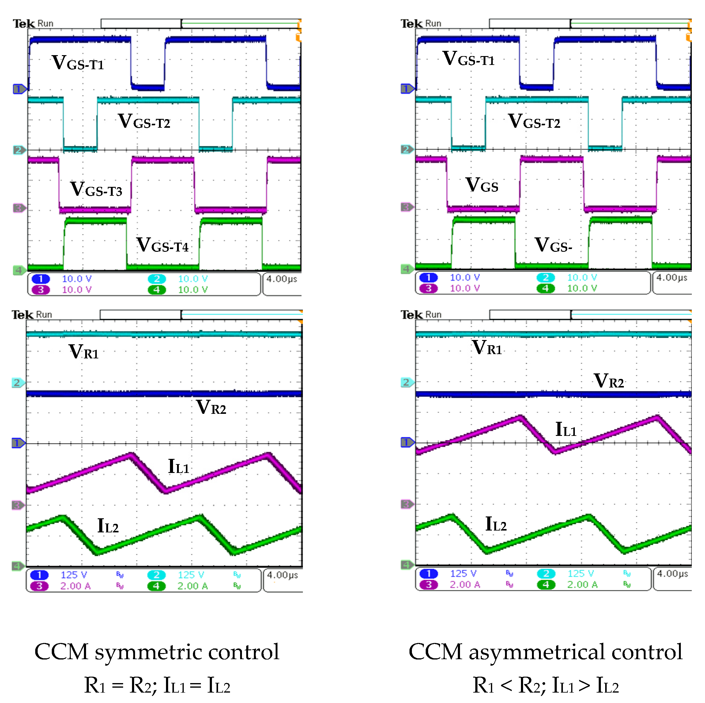
2.2. CCM Operation of the Proposed Converter

Considering the CCM operation, Figure 4 shows the steady-state waveforms for the inductor voltage and current at a duty cycle D larger and smaller than 0.5. For a duty cycle D larger than 0.5, the voltage ratio of the proposed converter can easily be deduced by the classic boost converter analysis approach [34], where the average inductor voltage equation is:
V in D + ( V in V C 1 ) ( 1 D ) = 0
where the capacitors C1 and C2 voltages are:
V C 1 = V C 2 = V out 2
The deduced voltage gain is given as:
V out V in = 2 ( 1 D )
Working at a duty cycle D smaller than 0.5, the average inductor voltage equation is:
V in D + ( V in V C 1 ) 0.5 V C 1 ( 0.5 D ) = 0
Thus, for this condition, the voltage gain can be expressed as:
V out V in = 2 D + 1 ( 1 D )
Considering (3) and (5), Figure 5 shows the DC conversion ratio M(D), of the proposed IDBIC converter for CCM operation in conjunction with the regular boost converter gain.

2.3. DCM Operation of the Proposed Converter

2.3.1. Case 1

Figure 6 shows the steady-state waveforms of inductor voltage and current for DCM operation in Case 1, where three different time intervals (D, D1, and D2) can be observed in a switching period. These waveforms are specific to the regular DCM boost converter [34].
From the average inductor voltage equation, the time interval defined by the time D1 in Figure 6 can be expressed as:
D 1 = 2 V in D V out 2 V in
Considering the output C1 capacitor charge balance, the converter load resistance R, the current area A from Figure 6, and the peak current ipk, the diode D1 average current equation can be described as:
i D 1 = 1 T s A = 1 T s ( 1 2 i pk D 1 T s ) = V in DD 1 T s 2 L 1 = 2 V C 1 R
By substituting the time interval D1 into (7), the voltage gain in DCM Case 1 becomes:
V out V in = ( 2 + 4 + 8 D 2 K ) 2
where:
K = 2 L 1 RT s
Using (8) and different values of the parameter K, Figure 7 shows the DC conversion ratio, M(D,K), of the IDBIC boost converter for DCM Case 1.

2.3.2. Case 2

This DCM working case is illustrated in Figure 8, in which the converter is working at a duty cycle smaller than 0.5, where four different time intervals (D, D1, D2, and D3) can be observed, and the inductor current has two falling slopes. For this operation mode, the average current of the diode D1 can be expressed using the current represented by the area A and the output capacitor C1 charge balance.
Using the average inductor voltage equation, the expression of the time interval D2 defined in Figure 8 is obtained:
D 2 = V in V C 1 ( D + D 1 ) D 1
Using the output C1 capacitor charge balance, the converter load resistance R, and the current area A from Figure 8, the diode D1 average current equation can be expressed as:
i D 1 = 2 V C 1 R = 1 T S A
By substituting the time interval defined by D2 into the capacitor C1 charge balance (11), the result is:
2 KV C 1 2 + V C 1 V in D 1 2 V in ( D + D 1 ) = 0
Knowing that the time interval D1 is 0.5, the voltage ratio of the converter becomes:
V out V in = 0.5 2 + 0.5 4 + 8 K ( D + 0.5 ) 2 K
Using (13) and different values of the parameter K, Figure 9 shows the DC conversion ratio, M(D, K), of the IDBIC boost converter for DCM Case 2.

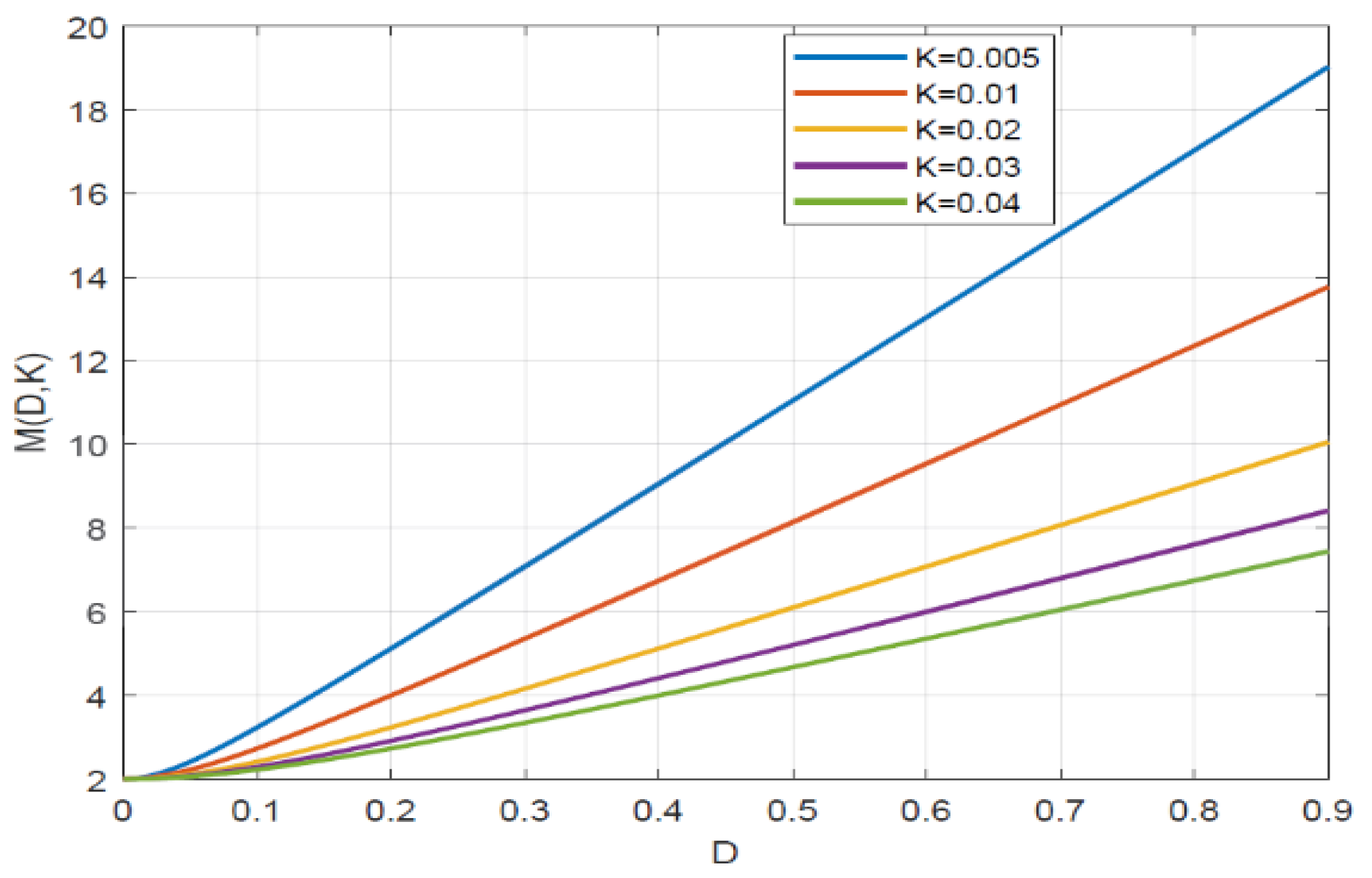
2.4. DCM–CCM Boudary Limit

In Figure 10, the DCM–CCM boundary limit is presented. Using the voltage gain Equations (3) and (8), the plot was obtained for D larger than 0.5, which complies with (14). For D smaller than 0.5, Equations (5) and (13) were used, and the evolution of the parameter Kcrt is defined by (15).
K crt ( D ) = D ( 1 D ) 2 2
K crt ( D ) = ( 1 D ) ( 1 + 2 D 4 D 2 ) 4 ( 2 D + 1 )

3. Simulation and Practical Implementation

Figure 11 and Figure 12 introduce the PLECS simulation and practical measurements for the discontinuous conduction mode (DCM) and continuous conduction mode (CCM) of the proposed IDBIC converter in the symmetrical operation of the two integrated boost converters. The gate-source command voltages of the transistors (T1, T2, T3, T4) are represented by VGS-T1, VGS-T2, VGS-T3, and VGS-T4. The drain-source voltages on all transistors are shown as VDS-T1, VDS-T2, VDS-T3, and VDS-T4. The inductors’ currents, IL1 and IL2, are illustrated as well. The command signals VGS-T1 and VGS-T2 are pulse width modulation signals (PWM), normally used in the regular interleaved boost converter with a 180° phase shift between the two signals. The logic 1 (high value) of the gate signal VGS-T3 was obtained between the falling edges of the VGS-T1 and VGS-T2 signals. The gate signal VGS-T4 was obtained by inverting the signal VGS-T3. A compulsory deadtime is introduced for the T3 and T4 transistor gate signals.
As one can notice, no significant difference can be observed between the simulated and practical measurements. The main differences are obtained during the DCM modes when the inductors’ currents are zero. Because of the parasitic components associated with the switching devices and PCB layout, resonant and transient behavior can be observed during the practical measurements. Despite this phenomenon, it is important to note that no relevant negative effect was present in the working behavior of the converter.
To operate the integrated boost converters in an independent manner, a three-voltage level system with two loads is needed at the output, as one can notice in Figure 13, where the generic voltage control loops and the PWM signal generator are highlighted. This schematic is suitable for an asymmetric control of the converter in which the reference voltages Vref 1 and Vref 2 can have different values; thus, each integrated boost converter needs to operate independently.
The most common usage of the asymmetrical control is related to the energy balancing/interconnections in bipolar DC grids/applications. Thus, in this case, the voltage references Vref 1 and Vref 2 are equal. Considering different values for the R1 and R2 loads in the asymmetric mode, indicating different inductor currents, the independent operation of the two integrated boost converters is demonstrated. For an application in which the overall output voltage Vout must be regulated, a symmetrical control loop approach is sufficient, meaning that only one PI controller and one voltage reference Vref are needed.
Figure 14 presents the practical measurements for the symmetric and asymmetric control of the converter considering the control schematics presented in Figure 13. For this situation, the output voltage Vout is set at 400 V, and the voltages VR1 and VR2 are equal to 200 V. During CCM operation, the command signals are almost identical, while the inductor currents are equal for the symmetric control and have different values for the asymmetrical control.
Moreover, based on an application with 50 V and 100 V input voltages and a 400 V output DC voltage in symmetric operation mode, the efficiency measurements carried out with the Tektronix PA3000 power analyzer are illustrated in Figure 15. The laboratory test setup is presented in Figure 16. For the prototype, the components and some general test specifications are presented in Table 1. In addition, Table 2 comprises the generalized information regarding the main characteristics of the proposed converter, directly compared with actual non-isolated topologies usually found targeting the same applications.
For analyses in wide voltage range applications, the laboratory prototype testing setup from Figure 16 was developed using high-voltage transistors, which exhibit quite high internal resistances (0.23 Ω). As one can see in Figure 15, at a 50 V input voltage, the efficiency decreases at high powers because of the transistors’ conduction losses that become predominant.

4. Conclusions

This work emphasizes the development and analysis of an interleaved converter with independent operation of the two integrated boost converter stages, attaining at the output a three-level voltage structure. The symmetric and asymmetric operations were demonstrated, together with all possible CCM and DCM operations.
Although the prototype design is not fully optimized, the results are encouraging, and future improvements can be aimed at the selection of the electronic switching devices, analog components, and PCB design. The converter features good energy efficiency with twice the voltage gain of regular boost and interleaved topologies.
The proposed converter has no specific feature with outstanding performance, and in certain applications, a shortcoming of the converter could be that the output and input do not share a common ground. Moreover, the complexity of the proposed structure can be considered a drawback, but by increasing the number of power electronics applications and particularities, alternative approaches will increase as well (Table 2). Compared with these solutions, the general number of components in the proposed converter is not very high. Nevertheless, considering all the combined characteristics, namely the interleaved property, high gain, good efficiency, low voltage stress, output with three-voltage levels, and especially the independent control of the integrated electronic structures, this converter is an engaging solution for PV optimizers/microinverters and battery energy management systems. Hence, thorough analytical and experimental studies are foreseen in future work to validate the proposed structure in DC grid interconnections and other applications by finding the best performance and optimal command/control strategies.

Author Contributions

Conceptualization, V.M.S. and P.D.T.; formal analysis, S.I.S.; investigation, V.M.S., S.I.S. and A.M.P.; methodology, V.M.S. and P.D.T.; software, V.M.S. and L.N.P.; supervision, P.D.T.; validation, V.M.S., A.M.P. and N.C.S.; writing—original draft, V.M.S., S.I.S. and P.D.T.; writing—review and editing, V.M.S., S.I.S. and P.D.T. All authors have read and agreed to the published version of the manuscript.

Funding

This research was funded by the European Regional Development Fund through the Competitiveness Operational Program 2014–2020 Romania, grant number 16/01.09.2016, project title “High power density and high-efficiency micro-inverters for renewable energy sources—MICROINV.

Informed Consent Statement

Not applicable.

Data Availability Statement

Not applicable.

Conflicts of Interest

The authors declare no conflict of interest.

References

  1. Tostado-Veliz, M.; Leon-Japa, R.S.; Jurado, F. Optimal electrification of off-grid smart homes considering flexible demand and vehicle-to-home capabilities. Appl. Energy 2021, 298, 117184. [Google Scholar] [CrossRef]
  2. Diaz-Saldierna, L.; Leyva-Ramos, J. High Step-Up Converter Based on Non-Series Energy Transfer Structure for Renewable Power Applications. Micromachines 2021, 12, 689. [Google Scholar] [CrossRef]
  3. Zhang, H.; Chen, Y.; Park, S.-J.; Kim, D.-H. A Family of Bidirectional DC–DC Converters for Battery Storage System with High Voltage Gain. Energies 2019, 12, 1289. [Google Scholar] [CrossRef] [Green Version]
  4. Ahmad, J.; Zaid, M.; Sarwar, A.; Lin, C.-H.; Ahmad, S.; Sharaf, M.; Zaindin, M.; Firdausi, M. A Voltage Multiplier Circuit Based Quadratic Boost Converter for Energy Storage Application. Appl. Sci. 2020, 10, 8254. [Google Scholar] [CrossRef]
  5. Lai, C.-M.; Yang, M.-J. A High-Gain Three-Port Power Converter with Fuel Cell, Battery Sources and Stacked Output for Hybrid Electric Vehicles and DC-Microgrids. Energies 2016, 9, 180. [Google Scholar] [CrossRef] [Green Version]
  6. Huang, H.; Balasubramaniam, S.; Todeschini, G.; Santoso, S. A Photovoltaic-Fed DC-Bus Islanded Electric Vehicles Charging System Based on a Hybrid Control Scheme. Electronics 2021, 10, 1142. [Google Scholar] [CrossRef]
  7. Malik, M.Z.; Chen, H.; Nazir, M.S.; Khan, I.; Abdalla, A.N.; Ali, A.; Chen, W. A New Efficient Step-Up Boost Converter with CLD Cell for Electric Vehicle and New Energy Systems. Energies 2020, 13, 1791. [Google Scholar] [CrossRef] [Green Version]
  8. Revathi, B.S.; Mahalingam, P.; Gonzalez-Longatt, F. Interleaved high gain DC–DC converter for integrating solar PV source to DC bus. Sol. Energy 2019, 188, 924–934. [Google Scholar] [CrossRef]
  9. Forouzesh, M.; Siwakoti, Y.P.; Gorji, S.A.; Blaabjerg, F.; Lehman, B. Step-Up DC–DC Converters: A Comprehensive Review of Voltage-Boosting Techniques, Topologies, and Applications. IEEE Trans. Power Electron. 2017, 32, 9143–9178. [Google Scholar] [CrossRef]
  10. Hu, X.; Li, L.; Li, Y.; Wu, G. Input-parallel output-series DC–DC converter for non-isolated high step-up applications. Electron. Lett. 2016, 52, 1715–1717. [Google Scholar] [CrossRef]
  11. Yan, Z.; Zeng, J.; Lin, W.; Liu, J. A Novel Interleaved Nonisolated Bidirectional DC–DC Converter with High Voltage-Gain and Full-Range ZVS. IEEE Trans. Power Electron. 2019, 35, 7191–7203. [Google Scholar] [CrossRef]
  12. Ahmad, J.; Zaid, M.; Sarwar, A.; Lin, C.-H.; Asim, M.; Yadav, R.; Tariq, M.; Satpathi, K.; Alamri, B. A New High-Gain DC–DC Converter with Continuous Input Current for DC Microgrid Applications. Energies 2021, 14, 2629. [Google Scholar] [CrossRef]
  13. Frivaldsky, M.; Hanko, B.; Prazenica, M.; Morgos, J. High Gain Boost Interleaved Converters with Coupled Inductors and with Demagnetizing Circuits. Energies 2018, 11, 130. [Google Scholar] [CrossRef] [Green Version]
  14. Choi, S.; Agelidis, V.; Yang, J.; Coutellier, D.; Marabeas, P. Analysis, design and experimental results of a floating-output interleaved-input boost-derived DC–DC high-gain transformer-less converter. IET Power Electron. 2011, 4, 168. [Google Scholar] [CrossRef]
  15. Li, Q.; Huangfu, Y.; Xu, L.; Wei, J.; Ma, R.; Zhao, D.; Gao, F. An Improved Floating Interleaved Boost Converter with the Zero-Ripple Input Current for Fuel Cell Applications. IEEE Trans. Energy Convers. 2019, 34, 2168–2179. [Google Scholar] [CrossRef]
  16. Dusmez, S.; Hasanzadeh, A.; Khaligh, A. Comparative Analysis of Bidirectional Three-Level DC–DC Converter for Automo-tive Applications. IEEE Trans. Ind. Electron. 2015, 62, 3305–3315. [Google Scholar] [CrossRef]
  17. Ganjavi, A.; Ghoreishy, H.; Ahmad, A.A. A Novel Single-Input Dual-Output Three-Level DC–DC Converter. IEEE Trans. Ind. Electron. 2018, 65, 8101–8111. [Google Scholar] [CrossRef]
  18. Chen, J.; Hou, S.; Sun, T.; Deng, F.; Chen, Z. A New Interleaved Double-Input Three-Level Boost Converter. J. Power Electron. 2016, 16, 925–935. [Google Scholar] [CrossRef]
  19. Tang, Y.; Wang, T.; He, Y. A Switched-Capacitor-Based Active-Network Converter Wit High Voltage Gain. IEEE Trans. Power Electron. 2014, 29, 2959–2968. [Google Scholar] [CrossRef]
  20. Marzang, V.; Hosseini, S.H.; Rostami, N.; Alavi, P.; Mohseni, P.; Hashemzadeh, S.M. A High Step-Up Nonisolated DC–DC Converter with Flexible Voltage Gain. IEEE Trans. Power Electron. 2020, 35, 10489–10500. [Google Scholar] [CrossRef]
  21. Maheri, H.M.; Babaei, E.; Sabahi, M.; Hosseini, S.H. High Step-Up DC–DC Converter with Minimum Output Voltage Ripple. IEEE Trans. Ind. Electron. 2017, 64, 3568–3575. [Google Scholar] [CrossRef]
  22. Zhang, Y.; Gao, Y.; Zhou, L.; Sumner, M. A Switched-Capacitor Bidirectional DC–DC Converter with Wide Voltage Gain Range for Electric Vehicles with Hybrid Energy Sources. IEEE Trans. Power Electron. 2018, 33, 9459–9469. [Google Scholar] [CrossRef]
  23. Haji-Esmaeili, M.M.; Babaei, E.; Sabahi, M. High Step-Up Quasi-Z Source DC–DC Converter. IEEE Trans. Power Electron. 2018, 33, 10563–10571. [Google Scholar] [CrossRef]
  24. Li, K.; Hu, Y.; Ioinovici, A. Generation of the Large DC Gain Step-Up Nonisolated Converters in Conjunction with Renewable Energy Sources Starting from a Proposed Geometric Structure. IEEE Trans. Power Electron. 2017, 32, 5323–5340. [Google Scholar] [CrossRef]
  25. Salvador, M.A.; Lazzarin, T.B.; Coelho, R.F. High Step-Up DC–DC Converter with Active Switched-Inductor and Passive Switched-Capacitor Networks. IEEE Trans. Ind. Electron. 2018, 65, 5644–5654. [Google Scholar] [CrossRef]
  26. Salvador, M.A.; De Andrade, J.M.; Lazzarin, T.B.; Coelho, R.F. Nonisolated High-Step-Up DC–DC Converter Derived from Switched-Inductors and Switched-Capacitors. IEEE Trans. Ind. Electron. 2019, 67, 8506–8516. [Google Scholar] [CrossRef]
  27. Maroti, P.K.; Ranjana, M.S.B.; Prabhakar, D.K. A novel high gain switched inductor multilevel buck-boost DC–DC converter for solar applications. In Proceedings of the 2014 IEEE 2nd International Conference on Electrical Energy Systems (ICEES), Chennai, India, 7–9 January 2014; Institute of Electrical and Electronics Engineers (IEEE): Piscataway, NJ, USA, 2014; pp. 152–156. [Google Scholar]
  28. Lakshmi, M.; Hemamalini, S. Nonisolated High Gain DC–DC Converter for DC Microgrids. IEEE Trans. Ind. Electron. 2018, 65, 1205–1212. [Google Scholar] [CrossRef]
  29. Baskar, M.S.; Meraj, M.; Iqbal, A.; Padmanaban, S.; Maroti, P.K.; Alammari, R. High Gain Transformer-Less Dou-ble-Duty-Triple-Mode DC/DC Converter for DC Microgrid. IEEE Access 2019, 7, 36353–36370. [Google Scholar] [CrossRef]
  30. Maroti, P.K.; Al-Ammari, R.; Bhaskar, M.S.; Meraj, M.; Iqbal, A.; Padmanaban, S.; Rahman, S. A new Tri-Switching State Non-Isolated High Gain DC–DC Boost Converter for Microgrid Application. IET Power Electron. 2019, 12, 2741–2750. [Google Scholar] [CrossRef]
  31. Bhaskar, M.S.; Alammari, R.; Meraj, M.; Padmanaban, S.; Iqbal, A. A New Triple-Switched-Triple-Mode High Step-up Con-verter with Wide Range of Duty Cycle for DC Microgrid Applications. IEEE Trans. Ind. Appl. 2019, 55, 7425–7441. [Google Scholar] [CrossRef]
  32. Wang, F.; Lei, Z.; Xu, X.; Shu, X. Topology Deduction and Analysis of Voltage Balancers for DC Microgrid. IEEE J. Emerg. Sel. Top. Power Electron. 2016, 5, 672–680. [Google Scholar] [CrossRef]
  33. Teodosescu, P.D.; Suciu, V.M.; Szekely, N.C.; Pacuraru, A.M.; Bojan, M. Interleaved Buck-Boost Voltage Converter. OSIM Patent Application A2019 00915, 19 December 2019. [Google Scholar]
  34. Erickson, R.W.; Maksimovic, D. Fundamentals of Power Electronics, 2nd ed.; Kluwer: Norwell, MA, USA, 2001. [Google Scholar]
Figure 1. The electronic schematic of the proposed converter—IDBIC.
Applsci 11 05993 g001
Figure 2. Switching stages for the proposed IDBIC converter.
Applsci 11 05993 g002
Figure 3. Presumptive functioning waveforms and switching stage correlations.
Applsci 11 05993 g003
Figure 4. CCM inductor voltage and current waveforms.
Applsci 11 05993 g004
Figure 5. Classic boost converter (purple line) and IDBIC (for D < 0.5 the orange line and for D > 0.5 the blue line) DC conversion ratio M(D) in CCM.
Applsci 11 05993 g005
Figure 6. Inductor voltage and current steady-state waveforms—DCM Case 1.
Applsci 11 05993 g006
Figure 7. DC conversion ratio M (D, K) of the boost converter—DCM Case 1.
Applsci 11 05993 g007
Figure 8. Inductor voltage and current steady-state waveforms—DCM Case 2.
Applsci 11 05993 g008
Figure 9. DC conversion ratio M (D, K) of the boost converter—DCM Case 2.
Applsci 11 05993 g009
Figure 10. CCM–DCM boundary limit plot for D < 0.5 (orange line) and for D > 0.5 (blue line).
Applsci 11 05993 g010
Figure 11. PLECS Simulation results in DCM and CCM operation modes.
Applsci 11 05993 g011
Figure 12. Practical measurements of the proposed converter in DCM and CCM.
Applsci 11 05993 g012
Figure 13. The generic output voltage control loop and PWM generator.
Applsci 11 05993 g013
Figure 14. Practical measurements of the proposed converter in symmetrical and asymmetrical operation modes.
Applsci 11 05993 g014
Figure 15. Laboratory practical efficiency measurements.
Applsci 11 05993 g015
Figure 16. Laboratory test setup.
Applsci 11 05993 g016
Table 1. Prototype components and specifications.
ParametersValues
Input Voltage—VIN50 V–100 V
Output Voltage—VOUT400 V
Switching frequency—fs100 kHz
Max. Output Power—POUT480 W
Switches (T1–T4)C2M0280120D
Diodes (D1, D2)C3D02060A
Inductors (L1, L2)50 µH, RL = 21 mΩ
Capacitors (C1, C2)100 µF
Table 2. Converter characteristics comparison.
Ref.Voltage Gain (M)Normalized Voltage Stress across the PowerPout
[W]
Efficiency
[%] at
Vin [V]
Components
S*/D*/L*/
C*/C.I*/T*
Switches VS/VODiodes VD/VO
IDBIC2/(1 − d)1/M + 0.5
1/M
0.524094.25 @ 50 V
95.95 @100 V
4/2/2/
2/-/10
[15](1 + d)/
(1 − d)
(M + 1)/2M(M + 1)/2M24091.7 @ 24 V2/2/2/
4/2/10
[17]1/(1 − d)0.50.530095.9 @ 60 V4/2/2/
3/-/11
[18]2/(1 − d)0.50.532090.2 @ 48 V
95 @ 80 V
2/3/2/
3/-/10
[20](3 + d1 − d2)/(1 − d1 − d2)(M + 1)/4M
(M − 1)/2M
(M + 1)2M50093.4 @ 20 V
95.85 @ 30 V
3/4/2/
3/-/12
[21](1 + 5d)/
(1 − d)
(1 + 5M)/6M(M + 1)/M20095.9 @ 30 V6/9/6/
1/-/22
[22]2/(1 − d)0.5-30091.3 @ 50 V
94.3 @ 100 V
4/0/1/
4/0/9
[23]3/(1 − d)0.330.3315093.9 @30 V1/5/1/
5/0/12
[26](3 + d)/
(1 − d)
(M + 1)/4M(M + 1)/2M20096 @ 30 V2/3/-/
3/1/9
S*: switch, D*: diode, L*: inductor, C*: capacitor, C.I*: coupled inductor, T*: total of components, VO: output voltage, VS: switch voltage, VD: diode voltage, Vin: input voltage, Pout: output power, d: duty cycle.
Publisher’s Note: MDPI stays neutral with regard to jurisdictional claims in published maps and institutional affiliations.

