Review

Gas Sensors Based on Localized Surface Plasmon Resonances: Synthesis of Oxide Films with Embedded Metal Nanoparticles, Theory and Simulation, and Sensitivity Enhancement Strategies

1
Centre of Physics (CF-UM-UP), University of Minho, 4710-057 Braga, Portugal
2
International Iberian Nanotechnology Laboratory, 4715-330 Braga, Portugal
*
Author to whom correspondence should be addressed.
Appl. Sci. 2021, 11(12), 5388; https://doi.org/10.3390/app11125388
Submission received: 5 May 2021 / Revised: 31 May 2021 / Accepted: 8 June 2021 / Published: 10 June 2021
(This article belongs to the Special Issue Optical Sensors and Gauges Based on Plasmonic Resonance)

Abstract

:
This work presents a comprehensive review on gas sensors based on localized surface plasmon resonance (LSPR) phenomenon, including the theory of LSPR, the synthesis of nanoparticle-embedded oxide thin films, and strategies to enhance the sensitivity of these optical sensors, supported by simulations of the electromagnetic properties. The LSPR phenomenon is known to be responsible for the unique colour effects observed in the ancient Roman Lycurgus Cup and at the windows of the medieval cathedrals. In both cases, the optical effects result from the interaction of the visible light (scattering and absorption) with the conduction band electrons of noble metal nanoparticles (gold, silver, and gold–silver alloys). These nanoparticles are dispersed in a dielectric matrix with a relatively high refractive index in order to push the resonance to the visible spectral range. At the same time, they have to be located at the surface to make LSPR sensitive to changes in the local dielectric environment, the property that is very attractive for sensing applications. Hence, an overview of gas sensors is presented, including electronic-nose systems, followed by a description of the surface plasmons that arise in noble metal thin films and nanoparticles. Afterwards, metal oxides are explored as robust and sensitive materials to host nanoparticles, followed by preparation methods of nanocomposite plasmonic thin films with sustainable techniques. Finally, several optical properties simulation methods are described, and the optical LSPR sensitivity of gold nanoparticles with different shapes, sensing volumes, and surroundings is calculated using the discrete dipole approximation method.

1. Overview on Gas Sensors

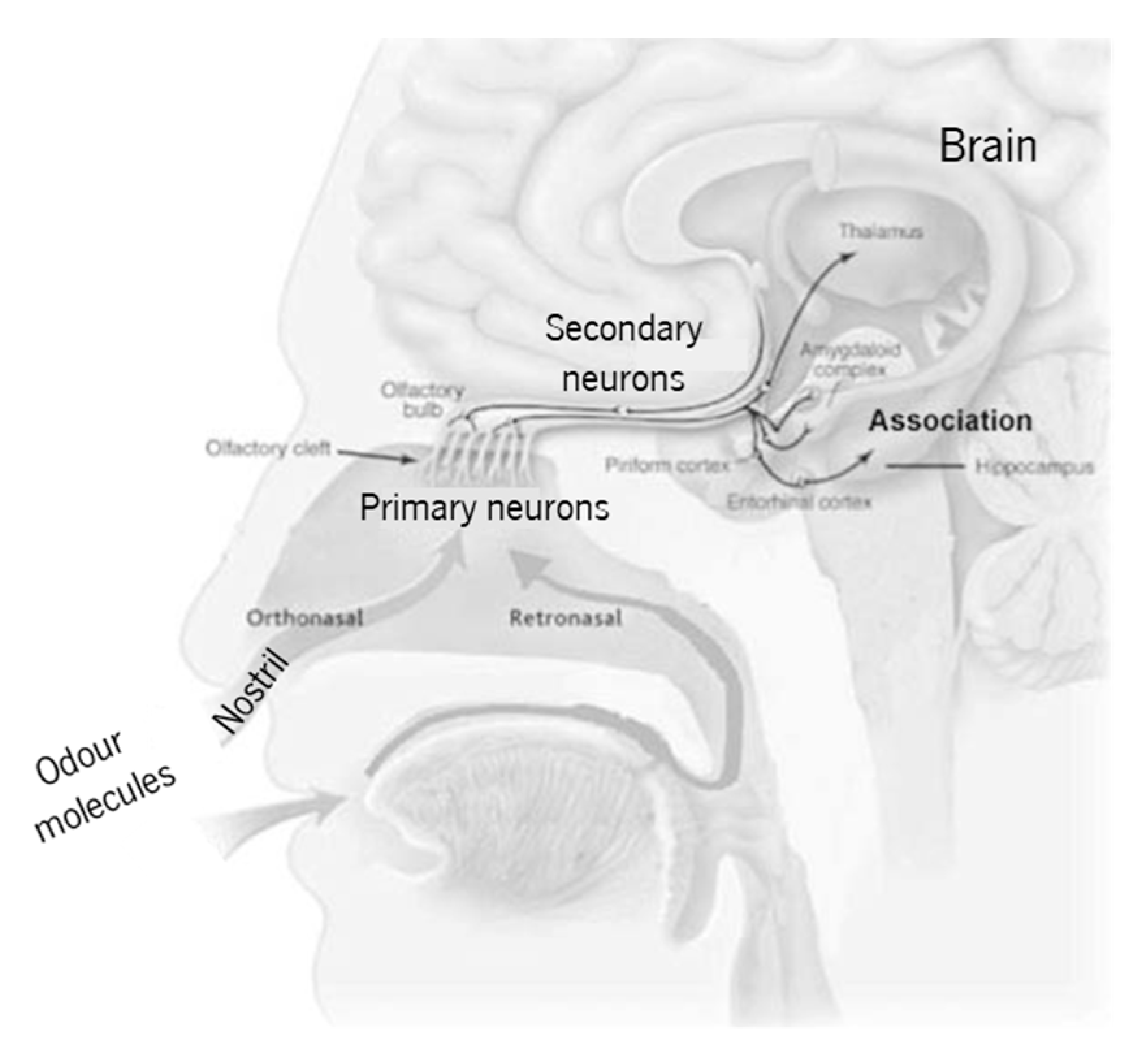
1.1. The Human Olfactory System

The human olfactory system (Figure 1) is used to evaluate the quality of food, drinks, perfumes, cosmetics, and chemical products. Unfortunately, the nose is capable of sensing only a small part of the available chemical species in air. Furthermore, the sensation, perception, and detection limit depend upon each person’s anatomy, experience, and memory. For these reasons, and in order to find reliable alternatives to the nonportable gas chromatography and mass spectrometry analytical techniques, portable gas sensors, also known as electronic-nose (e-nose) systems, have been the focus of several research projects [1]. These e-nose systems found their inspiration on the human olfactory system, as compared in Table 1. It consists of (i) a system to feed the gas (to mimic the nose), (ii) a sensor array (to mimic primary neurons in the cribriform plate), (iii) data preprocessing (to mimic secondary neurons), and (iv) the analysis and pattern recognition system (mimicking the brain). The e-nose is thus a collection of different individual gas sensors that work together to give an overall signal that will allow for a pattern recognition, which is a characteristic of the chemical species of interest.

1.2. Research Background on Gas Sensors

The first demonstration that a semiconductor (germanium, Ge) modifies its resistance depending on the surrounding atmosphere was made by Brattain and Bardeen in 1953 [3]. Their experimental schematics and monitoring example with oxygen are represented in Figure 2a-i,a-ii. In 1954, Heiland [4] described that metal oxides such as zinc oxide (ZnO) modify their semiconducting properties with a change in the partial pressure of oxygen in the surrounding atmosphere. The first gas sensing system was reported in 1964 by Wilkens and Hartman [5], which electronically mimicked the olfactory process (e-nose) using oxidation–reduction reactions of several odorants on distinct microelectrodes Figure 2b. In 1971, Taguchi patented the first gas sensing device, using tin dioxide (SnO2) as the sensitive material [6].
In the 1980s, the field of semiconductor sensors underwent a significant expansion [7] that led to the appearance of dedicated international peer reviewed journals such as Sensor Review, in 1981 (Emerald Group Publishing Ltd.) and Sensors and Actuators, in 1989 (Elsevier). However, the study of portable gas sensing systems only made its rapid progress since the publication in 1994 of a review on the e-nose, by Gardner and Bartlett [8].
Molecules interact with thin film sensors by adsorption (physisorption or chemisorption) or chemical reaction. These processes lead to a physical change in the film (sensor) that can be detected by variations in conductivity [8,9], mass [10], work function [11], or an optical property [12,13,14,15,16,17,18,19,20,21].
Most of the researched and established sensors use the conductivity change (Figure 3) of a given material as a signal, but they have low specificity, are susceptible to electrical noise, and the wiring needed complicates their implementation in some harsh environments. With the development of new technologies for the production of high quality optoelectronic components, optical sensors have undergone a large development over the past decades [22]. Optical sensors show excellent characteristics of sensitivity, selectivity, long lifetime, and fast response [6]. Therefore, they have attracted a great deal of attention for analytical applications, such as environment, industrial, and health monitoring. Furthermore, they have a straightforward working principle and simple hardware configuration, consisting of the sensing platform, a light source, optical fibres, a light detector, a processing unit, and pattern recognition software [22,23], following the same scheme of Figure 1b. The sensing mechanism is based on detecting a change in the light beam (frequency or wavelength, polarization, phase, or intensity) when the gas molecules interact with the sensing platform.

1.3. World Market

Nanomaterial-based sensors are a hot topic currently, especially for massive volume applications in the industrial, healthcare, consumer, and motor vehicle sectors, since they substantially reduce the size of the devices, with high-sensitivity, shorter response time, and real-time monitoring capabilities [24]. The world market for chemical sensors is projected to reach EUR 36,100 million by the year 2024 [25], with a growing demand that will be fuelled by new applications for established sensor products, product innovation, and falling cost of high-performance sensors. In particular, gas sensors are expected to reach 1400 million by the year 2024 (of which EUR 360 million in Europe) [26], powered by automotive, smart cities, building automation, medical, and other industrial applications (summary in Table 2). The main objective of these sensors is the detection of species that are “odourless” for humans, which can be harmful when their concentration is critical (such as carbon monoxide, CO [27,28]); below a certain limit (such as oxygen, O2 [29]); or dangerous when they are both volatile and inflammable (such as ethanol, C2H6O, or others [30]).
Hence, the development of new generations of optical gas sensors, tailored at the nanoscale to respond to various environments, has been increasing, thus imposing the exploitation of new sustainable production techniques and simulation models to achieve their best performance. This work contributes with the theory, simulation, and production of nanocomposite thin films consisting of an oxide matrix with embedded noble metal nanoparticles using reactive magnetron sputtering, along with strategies to enhance the sensitivity of these thin films.

2. Towards Optical Gas Sensing: Plasmonic Nanoparticles

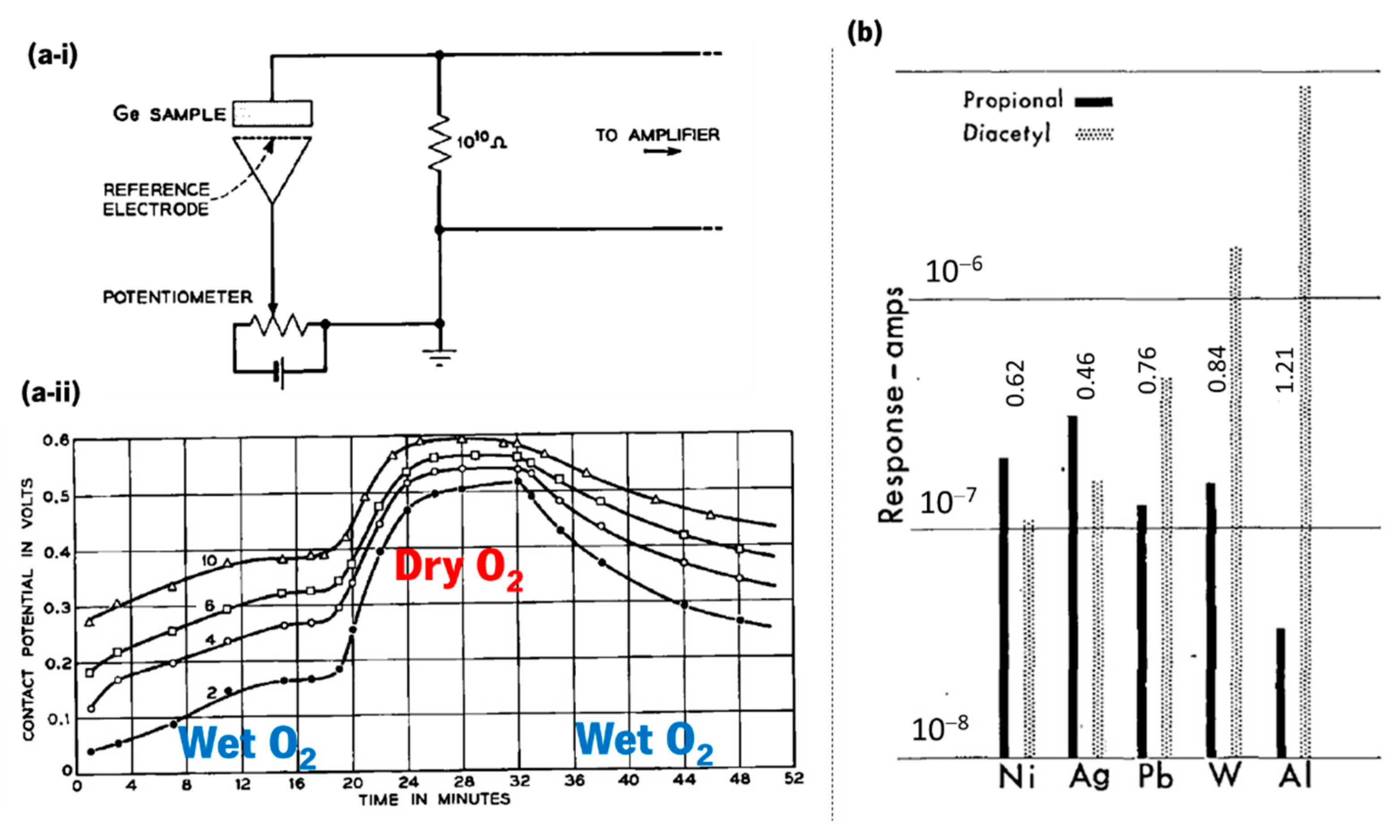
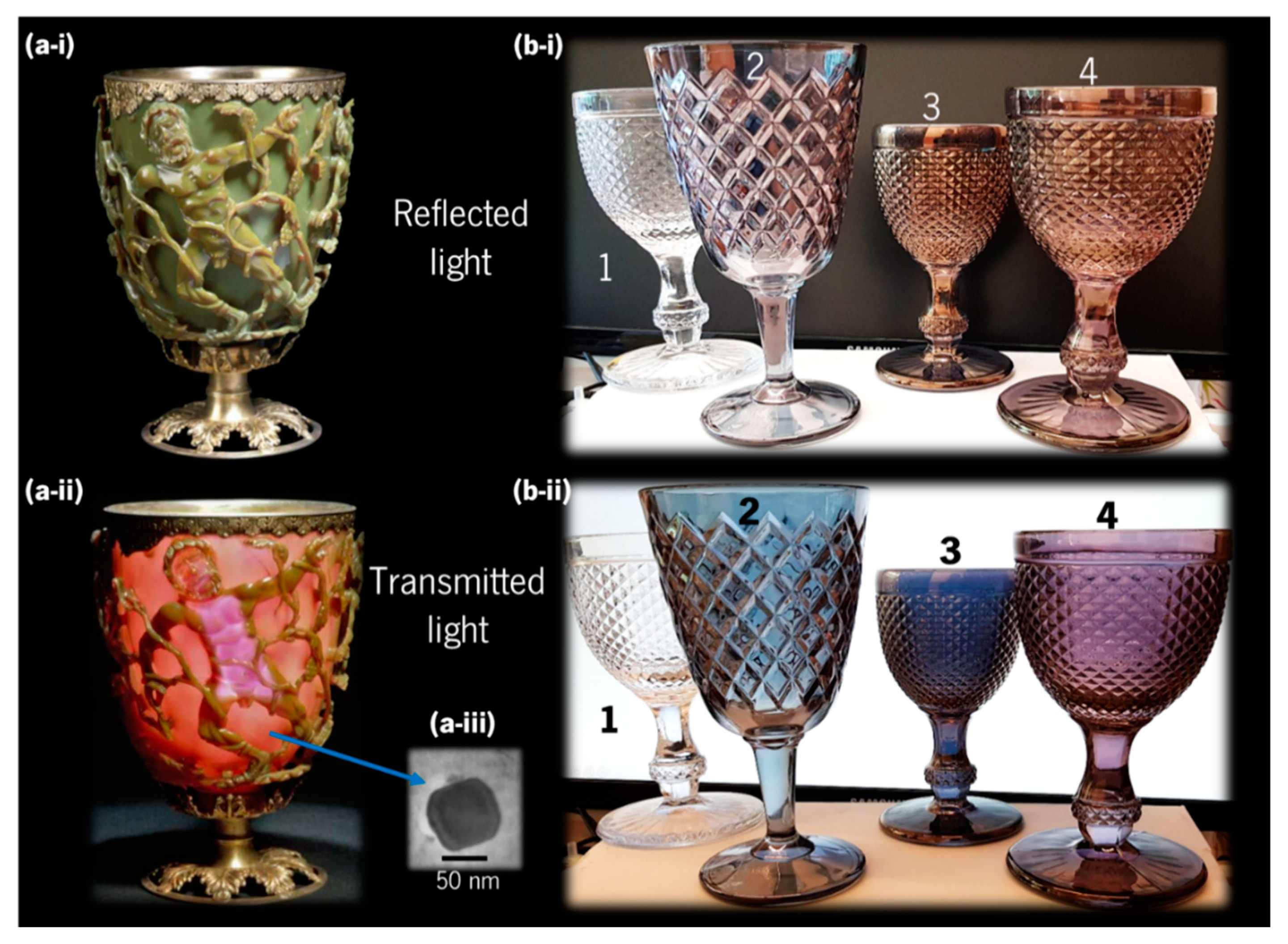
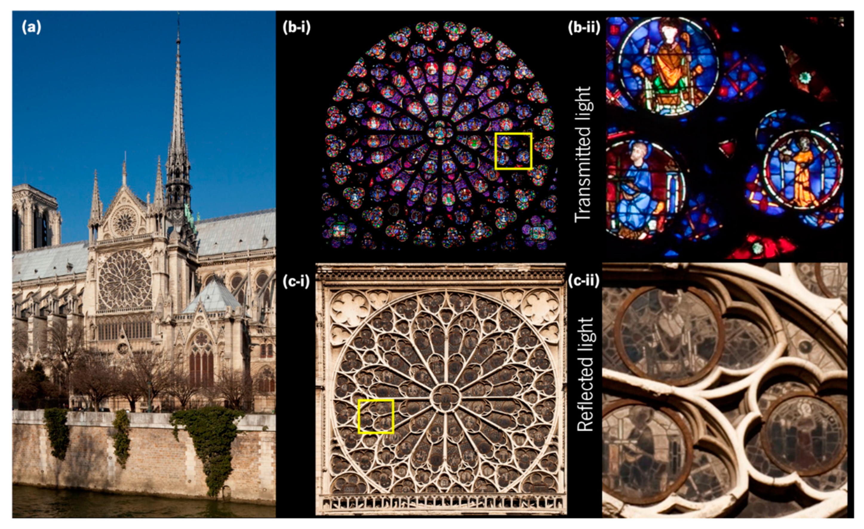
2.1. Ancient Stained Glass

Noble metals such as gold (Au) and silver (Ag) have been used since antiquity for decorative applications, and currently inspired several other practical uses in different scientific and technological areas [31]. Among several examples where noble metal-based colours can be found, the most ancient and fascinating one is the famous fourth century AD Lycurgus Cup displayed in the British Museum, London (Figure 4a).
In the 1960s, several chemical analyses were conducted on pieces of this Roman cup that revealed very small concentrations of gold (0.004 at.%) and silver (0.03 at.%) [32]. Later in the 1990s, with the advances in transmission electron microscopy (TEM) and energy dispersive X-ray spectroscopy (EDX), Barber and Freestone were able to explain the unusual optical properties such as a dichroic effect, i.e., the ability to change colour when illuminated from the outside or from within, looking as “opaque pea-green” in reflected light, and “deep wine-red” in transmitted light [32]. They found that Ag–Au alloy nanoparticles (Figure 4a-iii) with traces of copper (Cu) (Ag 66.2 at.%, Au 31.2 at.%, Cu 2.6 at.%) were responsible for the red transmission colour, while larger Ag nanoparticles were generating the green reflection colour [32]. Similar colours were demonstrated experimentally by Dekker et al. using solutions of Au and Ag nanoparticles [33]. Regarding the manufacture of the Lycurgus Cup, it is believed that it was made from a 15 mm-thick blown glass blank (a thick piece of glass with the overall shape of the final piece that undergoes additional decorations), and that the figures were cut, ground, and pressed to their actual shape [34]. Although the Roman glass industry was mature since the first century AD, the production method of the glass blank itself is still unclear. Modern methods of preparing colloidal noble metals were only developed after the 12th century and reported in the 17th century, so some theories speculate about successive grinding and melting of the glass, with several metals and metallic oxides added, in several steps. However, the existence of only six other broken pieces worldwide, from the same period, showing a similar but fainter dichroic effect has led some researchers to believe that the achievement of such an optical effect was most probably occasional, rather than the intentional work of a skilful craftsman [34,35].
With the advancements in nanotechnology, these optical effects can now be easily reproduced using thin film coatings deposited (e.g., by sputtering) directly on common glass, as exemplified in Figure 4b. In this case, the glasses were coated with a nanomaterial containing Au nanoparticles, embedded in an oxide matrix that protects them from mechanical abrasion, allowing to mimic the dichroic effect seen in ancient stained-glass. Cup number 1 is the uncoated reference, cup 2 and 3 were coated with Au nanoparticles embedded in titanium dioxide, TiO2, (cup 3 has a higher gold amount than cup 2), and cup 4 was coated with Au embedded in aluminium oxide (Al2O3). More details about the preparation of these thin films can be found elsewhere [36].
Another remarkable ancient use of gold and silver for decorative purposes is the stained-glass windows of medieval cathedrals. For example, in the “rose windows” of the gothic Notre-Dame Cathedral (Figure 5a) from the 13th century, in Paris, the presence of noble metal nanoparticles with different sizes and geometries embedded in the glass [31] yields magnificent colours that can be observed from inside the cathedral (transmitted light), Figure 5b-i,b-ii, while outside (reflected light) these colours appear very different, Figure 5c-i,c-ii.

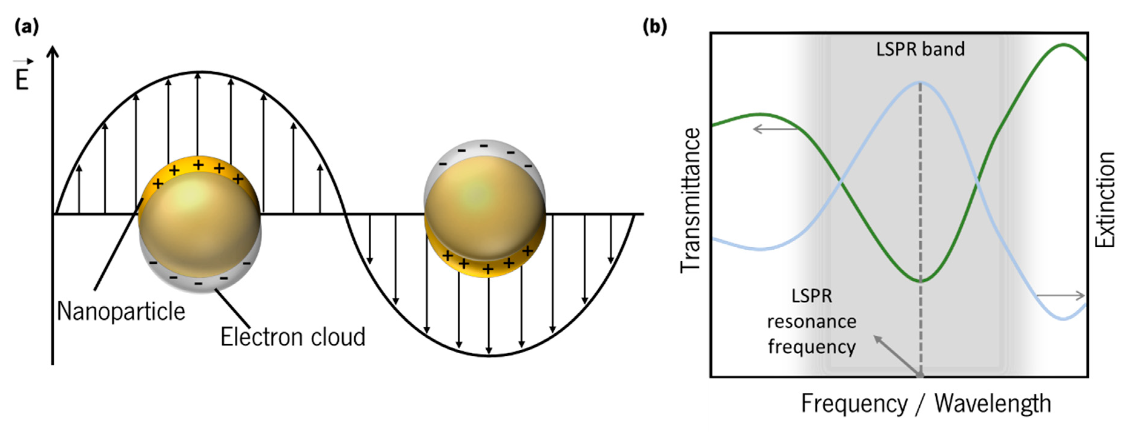
2.2. Background of Surface Plasmons

Although the aforementioned colour effects have been used for several centuries, their physical interpretation only started to gain relevance by the end of the 19th century and beginning of the 20th [37]. Particularly interesting was the theory proposed by Gustav Mie in 1908, who worked out a solution of Maxwell’s equations to calculate the extinction spectrum of a spherical particle illuminated by a time-harmonic electromagnetic field. The solution is an infinite series expansion with different terms corresponding to the n -th order multipoles of the sphere. The coefficients of this expansion are expressed in terms of the Riccatti–Bessel functions of the order n and the argument called the size parameter, x = 2 π n s a / λ 0 ( n s = ϵ s and a are the refractive index and the radius of the sphere, respectively, and λ 0 is the wavelength in vacuum). If x 1 , i.e., the particle is much smaller than the wavelength of the incident electromagnetic wave, only dipolar response may be considered, that is, the particle acts as an electrical dipole induced by the incident field (Figure 6a), p = ϵ m α E 0 , where ϵ m is the permittivity of the surrounding medium and α is particle’s polarizability,
α = 4 π a 3 ϵ s ϵ m ϵ s + 2 ϵ m .
If the sphere is metallic, the permittivity, ϵ s , is a complex function of the wavelength, so is the polarizability, and the particle both scatters and absorbs light. The extinction cross-section is a measure of both processes together, although the absorption dominates for small particles ( x 1 ) and it is given by [38]:
σ e = 2 π λ 0 Im   α .
The extinction depends on the dielectric functions of both the metal and host matrix, and the particle volume, v = 4 π a 3 / 3 .
This expression for the polarizability can be extended to the case of an ellipsoid, where α is a tensor with the principal components given by similar formulae,
α i = v ϵ s ϵ m ϵ m + η i ( ϵ s ϵ m ) ,   i = 1 ,   2 ,   3 ,
where η i are geometrical factors known as the depolarization coefficients [38,39]. They have the following property: i η i = 1. These formulae are commonly used to describe elongated nanoparticles, for instance, metallic nanorods.
Even though the classical treatment of Mie and its extensions to ellipsoids continue to be used to describe individual nanoparticles, it is not appropriate for more complex systems, where it is necessary to consider electromagnetic interactions between different parts of the system (e.g., different nanoparticles). Such systems, e.g., plasmonic nanostars [40] have more complex absorption and scattering spectra, which, in principle, can be understood by considering a set of interacting dipoles that can support collective electromagnetic modes. Such modes also can be excited by incident light.
In the 1950s R. H. Ritchie, who studied the characteristic energy losses of accelerated electron beams passing through thin films, triggered new developments on the subject at the experimental level, culminating in the demonstration, by Powell and Swan, of the existence of self-sustained collective excitations at metal surfaces, named thereafter as surface plasmons by Stern and Ferrell [41]. Using a similar experiment Ritchie, Otto, and Raether-Kretschmann demonstrated, independently, that propagating surface plasmons on a metal surface can also be excited by light [37]. It should be remembered that the propagating surface plasmons are characterized by a well-defined wavevector component along the surface, which is larger than any propagating photon of the same energy could have. The problem of wavevector matching can be bypassed by using a prism (so called Kretschmann and Otto configurations) or using surfaces with modulated conductivity [42]. It does not exist for confined geometries (e.g., for a spherical particle) because the wavevector is not well defined and its conservation in plasmon–light interaction is relaxed.
About two decades later, in 1974, Fleischmann, Hendra, and McQuillan reported, for the first time, the phenomenon of surface-enhanced Raman scattering (SERS) occurring on structured metallic surfaces and thus made a decisive contribution to the general interest in surface plasmons [43]. Since then, there have been significant advances in both theoretical and experimental research on surface plasmons, which led to the development of new simulation methods to calculate the optical properties of plasmonic systems [37,44,45,46] (more details in Section 5), and has delivered a relevant number of important applications [47,48].

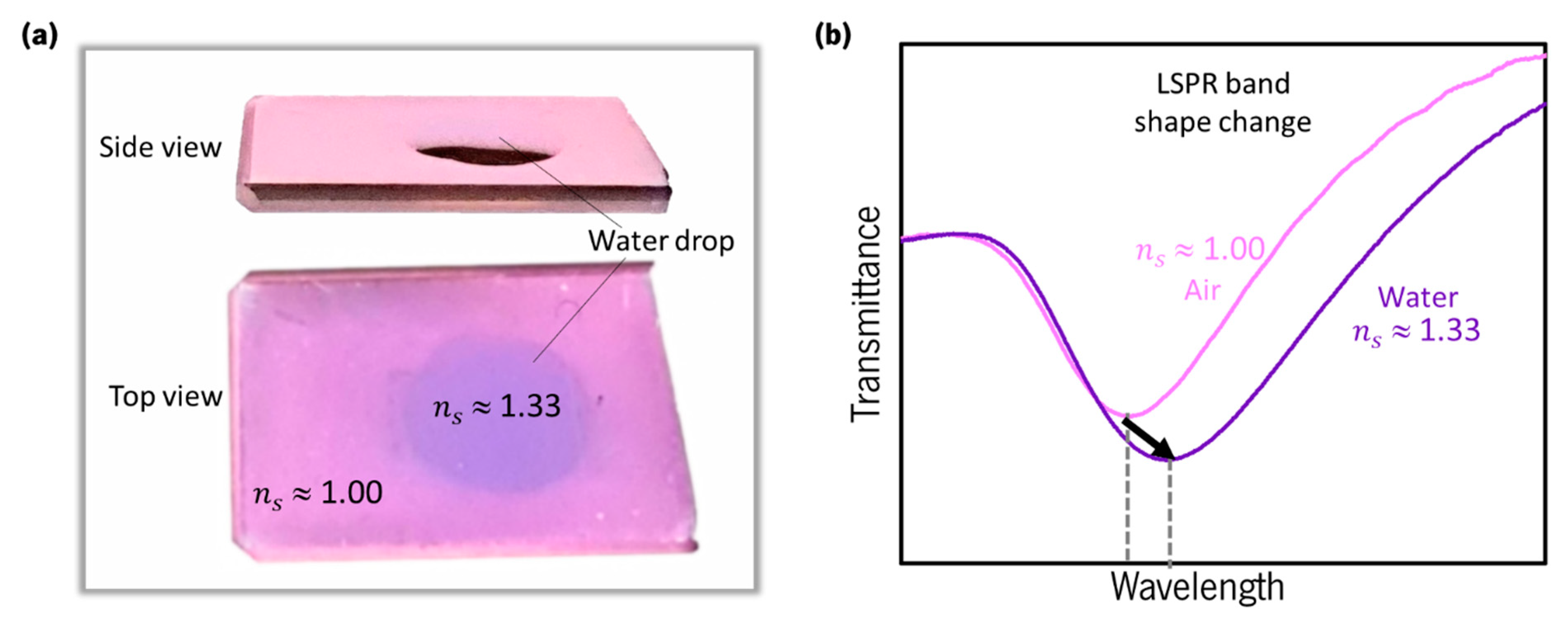
2.3. Localized Surface Plasmon Resonance (LSPR)

Noble metals (e.g., Au, Ag) are excellent electrical conductors due to the typically long mean free path of the electrons in the s-type conduction band. A quantum of their collective oscillations is called a plasmon. The term is also used to loosely refer to these kinds of elementary excitation, which are oscillations of the electron density accompanied by an electromagnetic field. Plasmons can arise in bulk materials (volume plasmons), or at the interface between two materials (surface plasmons–SPs) [49]. The excitation of SPs occurs when they interact with an incident electromagnetic field of frequency close to their natural oscillation frequency. SPs are divided into two main fundamental excitations: (i) surface plasmon polaritons (SPPs), which are evanescent electromagnetic waves coupled to the electron plasma of a metal and propagating along its surface [41,49,50], as already mentioned in the previous section; and (ii) localized surface plasmons (LSPs), Figure 6a, which are nonpropagating excitations of the conduction band electrons in subwavelength metallic nanostructures, coupled to a confined electromagnetic field [49,51,52,53].
To comply with energy and momentum conservation laws, SPPs cannot be excited directly by a propagating photon in air, since their momenta do not match [54], while LSPs have the advantage of coupling directly to photons. These frequency dependent coupling processes are commonly known as surface plasmon resonance (SPR) and localized surface plasmon resonance (LSPR), whether they occur, respectively, in a metal surface/dielectric interface, or in a metal nanoparticle or nanostructure. The LSPR band can be detected in an optical transmittance spectrum by a depression zone, and the LSPR resonance frequency corresponds to the maximum of the extinction (absorption + scattering) (Figure 6b). Thus, optical transmittance-LSPR (T-LSPR) is a simple technique by which the LSPs can be excited by the traversing light.
Different-order LSPRs are predicted by the Mie theory for a metallic sphere. The dipole resonance is determined by the pole of the particle polarizability, ϵ s + 2 ϵ m = 0 . Noteworthy is the dependence of the LSPR frequencies on the dielectric constant of the surrounding medium, which is the basis for the sensing applications of plasmonic nanoparticles. For a spheroidal nanoparticle, LSPRs can be split into two frequencies, corresponding to the poles of two unequal components of the polarizability tensor, α i [55]. Taking the noble metal permittivity within the simplest Drude model, the LSPR frequencies are given by:
ω p = ω p 1 + ( η | | 1 1 ) ϵ m ;   ω p = ω p 1 + ( η 1 1 ) ϵ m ,
where ω p is the plasma frequency of the bulk metal and η | | and η are the corresponding depolarization coefficients. The two resonances correspond to the electric field directed along or perpendicular to the longer axis of the spheroid, respectively. The separation in frequency between them can be very large for elongated nanoparticles (see Section 5.3).

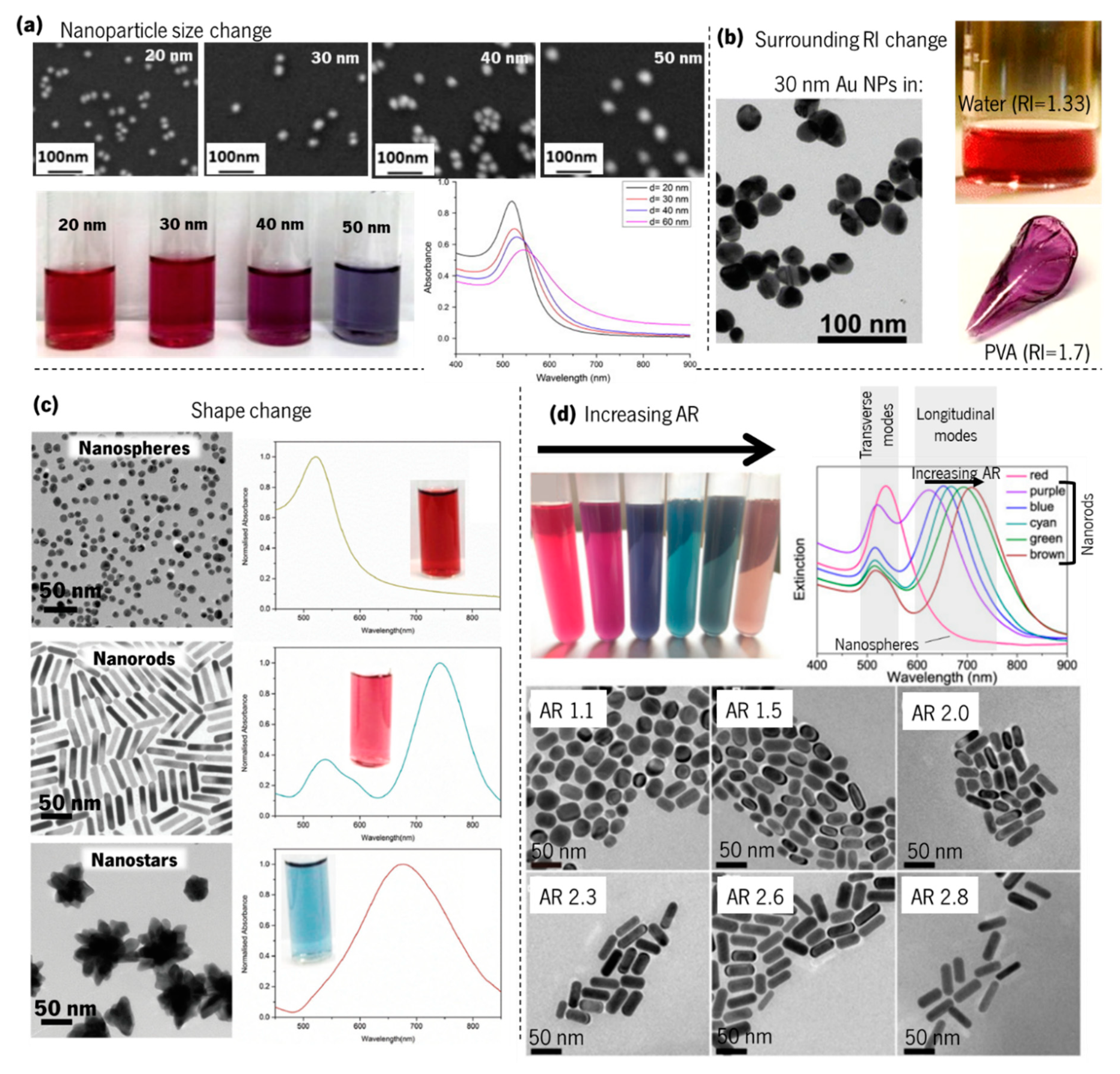
2.4. Gold Nanoparticles: LSPR Band Curvature and Applications

The plasmonic resonances are broadened because of several natural reasons, which include shape and size dispersion in nanoparticle ensembles, and the electron scattering in each individual particle. Bulk plasmons are damped mostly because of the electron–phonon interaction and in small particles there is an additional source of damping called surface scattering, for which it has been shown that it increases linearly with the inverse of the radius in the small size regime (less than 25 nm) [56]. All these factors result in a broadened LSPR band. Thus, the curvature of the band depends basically on the nature of the nanoparticles and their distribution, and on the surrounding dielectric function [51].
Although it may be counterintuitive, the awareness of the resonant properties of plasmonic metal nanoparticles is readily apparent to the naked eye. Since the nanoparticles absorb and scatter visible light, they can generate a wide palette of colours, depending on their concentration, geometries, and dimensions, and on their surroundings [57,58,59,60]. As can be seen in Figure 7a, by increasing the size of the Au nanoparticles (observed using scanning electron microscopy—SEM), the LSPR band shape changes smoothly, thus altering the colour [61]. On the other hand, if the “same” nanoparticles are embedded in different materials, the LSPR band resonance will be shifted to higher or lower wavelengths, whether the surrounding refractive index is higher or lower, thus changing the colour of the material. An example of this colour change is shown in Figure 7b when only the material surrounding the Au nanoparticles is changed, from a refractive index of 1.33 (water) to 1.7 (poly(vinyl alcohol), PVA) [62]. Moreover, by changing the shape of gold nanoparticles (Figure 7c) [58], from nanospheres to nanorods or nanostars (the shape is observed in the transmission electron microscopy, TEM, images), the LSPR band on the optical absorption spectra also changes, and hence the colour, from deep-red to sky-blue. Furthermore, the adjustment of the aspect ratio (AR) of gold nanoparticles from 1.1 to 2.8 [59] (Figure 7d) redshifts appreciably the longitudinal LSPR band ( ω p ), thus changing considerably the colour.
Beyond the already mentioned decorative field, several other applications based on the LSPR phenomenon have shown very promising impacts. As a matter of fact, due to their high sensitivity to the surrounding dielectric environment, plasmonic metal nanoparticles have received considerable attention over the past decade for sensing applications. Among them are the detection of biomolecules by plasmonic sensing [63,64,65,66,67,68,69,70] using several methods, as depicted in Figure 8a,b. To analyse the LSPR band curvature changes in sensing experiments, Rodrigues et al. [71] developed a software that calculates several parameters of the LSPR band, such as the (i) wavelength and transmittance coordinates of the optical transmittance spectrum minimum, (ii) several transmittance values at discrete wavelengths, and (iii) the (statistic) first central moments of the normalized spectral distribution.
Other examples that are still related to biomolecular detection are plasmon-enhanced fluorescence (PEF, Figure 8c) [72,73] and SERS [74,75,76]. Furthermore, plasmonic nanoparticles are currently used in several other fields, from the enhancement of absorbed light in solar cells [77,78,79,80] to biological imaging (Figure 8d) [81,82,83,84] and phototherapy of tumours (Figure 8e) [82,85,86].

3. Metal Oxides as Robust Platforms to Host Plasmonic Nanoparticles

To mechanically protect the Au nanoparticles and use environment-friendly deposition processes to obtain it, transparent metal oxides, or even metal nitrides, are often used as the “host” for the nanoparticles. The host matrix also allows for tuning the LSPR band since, on the one hand, it changes the refractive index surrounding the nanoparticles and, on the other hand, it may limit the size distribution [36]. Moreover, the host matrix micro- and nanostructure is of paramount importance to tailor the sensitivity to gas molecules. In fact, as mentioned in Section 1, oxide materials are recognized worldwide as being convenient platforms for gas sensing using electrical signals as transduction mechanisms. Two examples of metal oxides that could work as potentially suitable host matrices for gold nanoparticles are titanium dioxide (TiO2) and copper oxide (CuO).
Pure TiO2 is a transparent n-type semiconductor material, with a large bandgap varying between 3.0 and 3.4 eV [87,88,89,90,91]_ENREF_4. TiO2 is known for its biocompatibility, nontoxicity, chemical stability, high hardness, and high optical transmittance combined with a high refractive index that ranges between 2.4 and 2.9 [92,93,94,95]_ENREF_10. TiO2 exists in both amorphous and crystalline forms, with the most important phases anatase and rutile, both showing a tetragonal lattice structure [96]. Among these phases, anatase is known for its excellent photocatalytic activity [96,97,98], for antifogging and self-cleaning coating material for glasses [99,100], and it is kinetically stable at low temperatures. In the rutile form, TiO2 has good structural stability at high temperatures, together with a higher refractive index [101]. Conversely, in its amorphous form, TiO2 has high blood compatibility and thus it is often used in several types of biomedical applications [102]. In addition, TiO2 is widely used as a (chemical) gas sensor (Figure 9a) [103,104,105,106,107,108,109] and this is also a major reason why it is being explored for plasmonic sensing.
Pure CuO is a p-type semiconductor material with a band gap in the range 1.2–2.1 eV and a monoclinic crystal structure [87,111,112]. In recent years, it has attracted much interest due to its potential applications in several technological fields, such as catalysis [113,114,115], solar cells [116,117,118], electronics [119,120], and sensors [121,122,123]. In addition, CuO films have several unique features, such as low cost, nontoxicity, and abundant availability of constituents [124]. Due to these characteristics, CuO has been employed in the production of bio/chemical sensing devices (Figure 9b), operating by measuring conductivity changes induced by adsorption of molecules at its surface [110,121,125,126,127].

4. Preparation of Plasmonic Thin Film Sensors

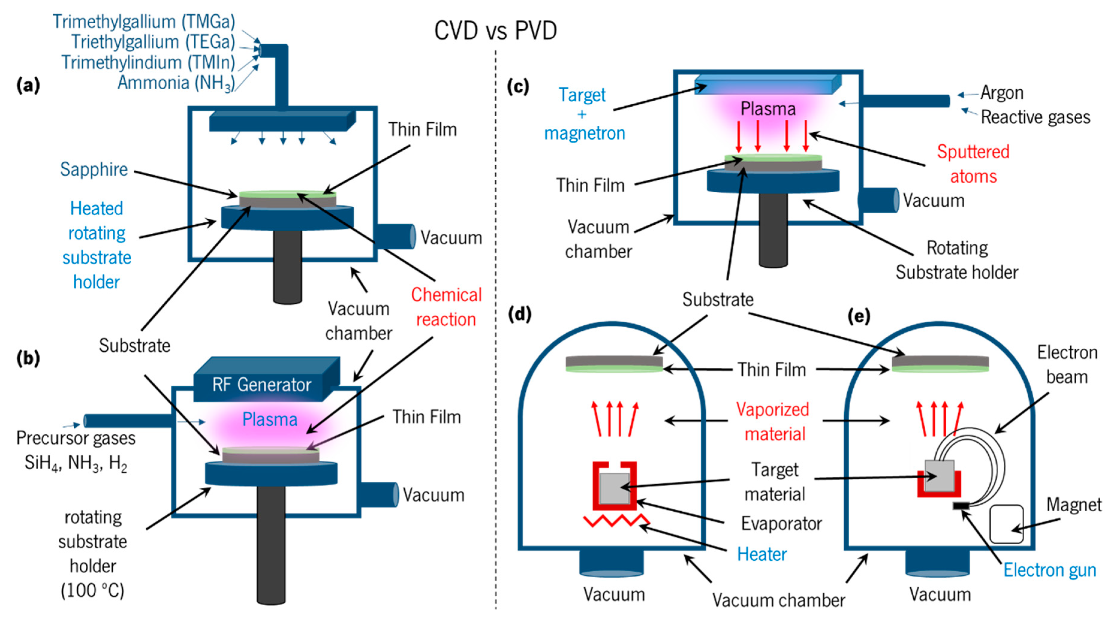
4.1. Thin Film Deposition Methods

The huge diversity of thin film materials available, and still to discover, implies the existence of several wet/dry, chemical/physical, and vacuum/atmospheric processing and fabrication techniques [128,129]. Regarding the scope of this work, the wet chemical deposition techniques are not discussed here; their overview can be found elsewhere, including the sol-gel [130,131], chemical bath [131,132], spray pyrolysis [133,134], electrophoretic deposition [135], and electroplating [136,137,138] techniques. Considering only dry vacuum deposition methods, it is possible to classify these techniques into two groups, physical and chemical processes [139].
In chemical methods, chemical reactions are needed to obtain the final thin film (Figure 10a,b), while physical methods cover the deposition techniques that depend on the ejection of the material from a source by evaporation or sputtering (Figure 10c–e).
Chemical vapour deposition (CVD) can be defined as a material synthesis method in which particles in the vapour phase react together to form a solid film in an energy-activated surface. The chemical reaction is a crucial characteristic of this method; therefore, besides the control of the usual deposition process variables, the related reactions must be well understood. Chemical reactions such as reduction, oxidation, and hydrolysis, among others, may occur. The activation energy may come from different sources, for example, heat, in conventional CVD (Figure 10a), or a plasma, in plasma enhanced CVD (PE-CVD) [140] (Figure 10b). When plasmas are used in CVD reactors to activate and partially decompose the reactants, the deposition will be possible at a temperature lower than conventional CVD. These plasmas are generated by using radiofrequency (RF) generators, as can be seen in Figure 10b. CVD processes are widely used in industry due to their versatility for depositing a large variety of elements and compounds covering a wide range of materials. Among these materials, metal oxides may be produced with a high degree of perfection and purity.
The advantages of physical methods are mostly related to dry processing, high purity and cleanliness, and compatibility with semiconductor integrated circuit processing, while being considered as green processes. However, there are certain disadvantages such as low deposition rates, difficult stoichiometry control, and high initial investments [140]. In physical vapour deposition (PVD) techniques, (i) the solid material to be deposited is physically transformed to a vapour phase, (ii) this vapour phase is transported through a low pressure volume from the source to the substrate, and (iii) the vapour condenses on the substrate to form the thin film [141]. The first stage (solid to vapour) is carried out by physical removal of surface atoms by particle-to-particle momentum transfer, in sputter deposition (Figure 10c), or by heating in evaporation deposition systems (Figure 10d,e). A large number of materials can be evaporated, and if the evaporation is undertaken in a vacuum system, then the evaporation temperature will be considerably reduced, and the impurities in the growing film will be minimized [140]. To evaporate materials in vacuum, the material holder must supply the vaporisation energy, while keeping its stability with an insignificant vapour pressure and dissociation, and without reacting chemically with the material of interest. The heating source may be a simple tungsten electrical resistive filament (Figure 10d) or an electron beam (Figure 10e).

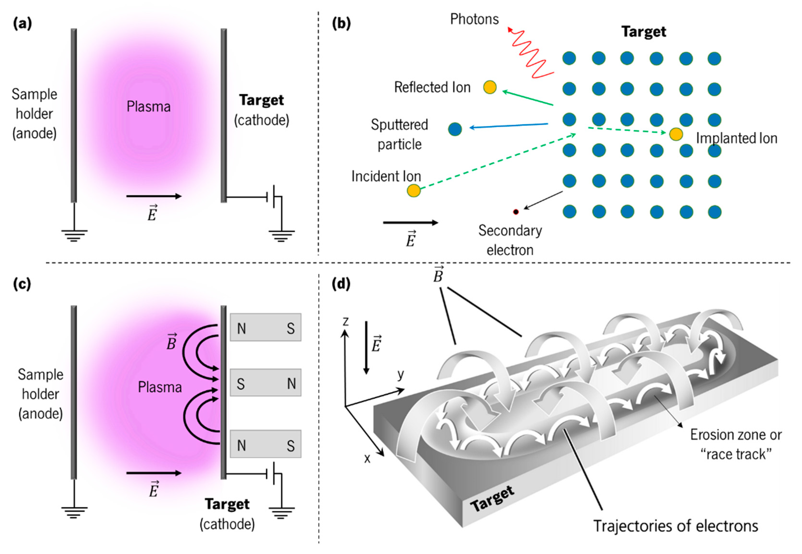
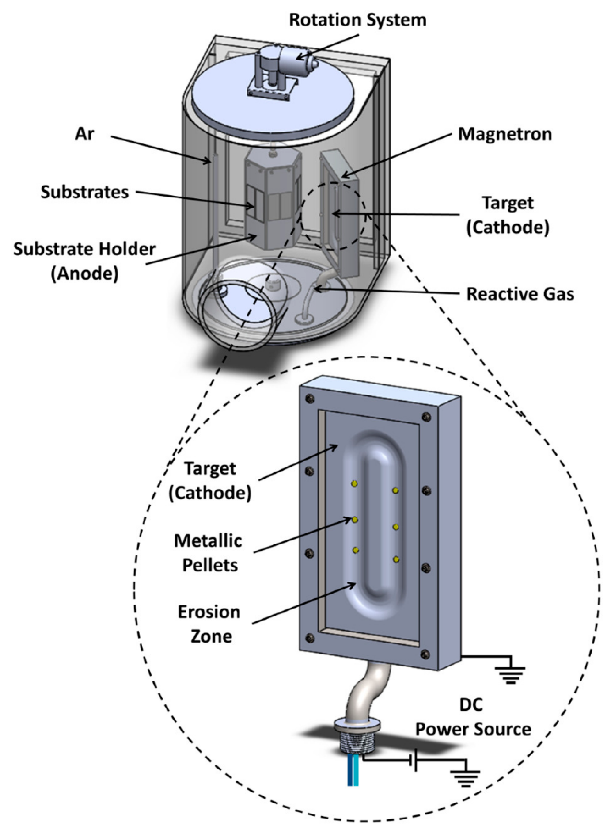
4.2. Reactive Magnetron Sputtering Deposition

Currently, sputtering is used in various fields of applications, for example, in the deposition of thin films, for surface etching, cleaning or activation, and in chemical analysis [142]. The industrial importance of sputtering includes semiconductor processing, surface finishing, jewellery, cutlery and optics, among others [143]. Since no chemical reactants are used and no waste is produced, this PVD process is also considered environmental friendly [144].
During the sputtering process, two main events occur after the introduction of a working gas and the application of an electric field: plasma generation and ion bombardment. After applying a negative potential to the cathode or “target” and grounding the anode or “sample holder”, an electric field ( E ) is generated (Figure 11a). Afterwards, the few existent electrons/ions (generated by natural processes such as cosmic rays or radioactive decay) are accelerated, leading to the creation of more charge carriers within the gas [145,146], i.e., the formation of a plasma (the concept of “plasma” was first described in 1928 by Irving Langmuir as the fourth state of matter [147]).
During the sputtering process, the ionized species that are accelerated in the electric field bombard the target. The bombardment causes the ejection of atoms and secondary electrons from the target surface, among other processes schematized in Figure 11b, such as photon emission, which makes the plasma visible. The secondary electrons that are ejected from the target play a fundamental role in maintaining the plasma. The electric field between the target and the sample holder induces an acceleration of the secondary electrons, and as they collide with neutral particles inside the vacuum chamber new charged carriers are created, and a steady-state plasma is developed [143]. The ejected target atoms are then deposited onto a substrate placed in front of the target, giving rise to a thin film [141].
Nevertheless, this basic sputtering process for thin film deposition initially only played a minor role compared to, e.g., thermal evaporation. Major drawbacks given were the low deposition rates of the process, the low ionization efficiency, inferior properties of the films, and substrate heating [149]. These limitations were overcome with the development of the magnetron [146].
The basic principle of magnetron sputtering is to impose a magnetic field ( B ) near the target (Figure 11c). The magnetron is a system of permanent magnets, with a specific orientation, placed behind the target. The introduction of a magnetic field confines the electron motion to the vicinity of the target (Figure 11d), increasing the probability of electron-ion/atom collisions [142]. Thus, the ionization efficiency increases, causing a higher plasma density near the cathode, which enhances the process efficiency (higher deposition rates) and hence the quality of the deposited films [143].
However, the plasma over the target surface is not uniform, so that the sputtering phenomena are much localized to a “preferential” erosion zone (Figure 11d) [148], sometimes using only about 30% of the whole target material. As the target is sputtered, its characteristics also change, so the deposition conditions such as the layer thickness and the film morphology are expected to change during the lifetime of the target [142]. To overcome this hurdle, moving targets/magnet systems have been developed, with almost 80% usage for flat targets [150], and more than 90% in cylindrical rotating targets [151].
Reactive magnetron sputtering is characterized by the addition of reactive gases, for example, oxygen (O2) and nitrogen (N2), to the “working” gas (usually argon, Ar). Those gases are mentioned as “reactive” since they are introduced to chemically bond to the sputtered atoms. In this way it is possible to produce complex metallic oxides/nitrides thin films with a specific stoichiometry, such as aluminium oxide (Al2O3), aluminium nitride (AlN), titanium dioxide (TiO2), copper oxide (CuO), and many more [146,152].
The magnetron sputtering systems used most employ a primary vacuum pump (e.g., oil-sealed rotary vane, diaphragm, or piston) to produce a medium vacuum, i.e., lower than 1 Pa in the deposition chamber. After this pressure is reached, a high/ultrahigh vacuum pump (e.g., turbomolecular, ion, oil diffusion, or cryogenic pump), backed up by a fore-vacuum pump (for example, the primary vacuum pump) produces a base pressure lower than 10−4 Pa in the deposition chamber.
When this pressure is reached, the working gas (e.g., Ar) and, if needed, the reactive gases (e.g., N2 or O2), are introduced (Figure 12) using mass flow controllers. Then, after configuring the desired parameters (e.g., current, potential, power, frequency, pulse width, time on, etc.), the power source (e.g., DC, RF, or pulsed DC power source) is turned on to generate and maintain the plasma, and the sputtering deposition process occurs.
In addition, to prepare nanocomposite thin films where Au nanoparticles are embedded in the oxide matrix, the sputtering target is initially modified with small pieces (disks/“pellets”) of the desired metal, as depicted in Figure 12.

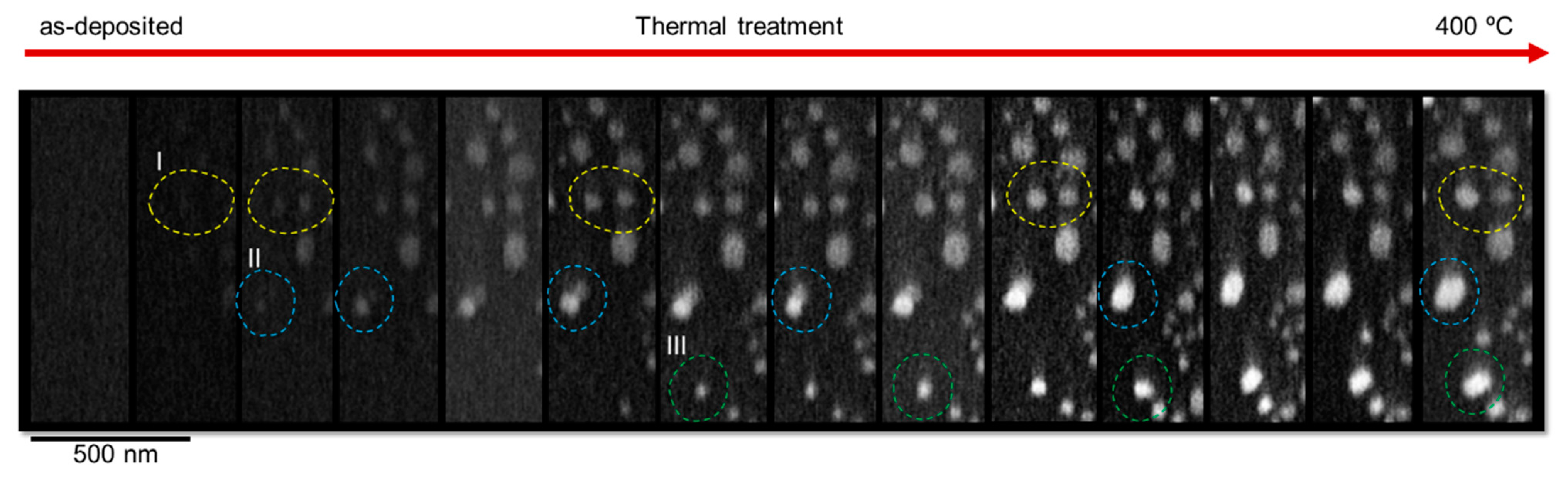
4.3. Thermal Annealing to Promote Gold Nanoparticle Growth

Once the nanocomposite thin films have been deposited, a post-deposition thermal treatment may be required to promote the growth of nanoparticles up to sizes that originate a LSPR band, measurable and observable in the transmittance spectrum. The growth of the nanoparticles from atoms initially dissolved in the matrix and distributed uniformly occurs through three main stages: (i) nucleation, when some new nanoparticles, formed by fluctuations, eventually reach a critical size and form stable nuclei; (ii) “normal growth” of the nuclei at the expense of dissolved matter; and (iii) Ostwald ripening (when small nanoparticles are dissolved and the atoms are transferred to larger nanoparticles) or coalescence (when two NPs are in contact and merge to form one larger NP) [154,155]. Magnetron sputtering deposition typically originates gold clusters/nanoparticles with sizes below 10 nm dispersed throughout the matrix, meaning that kinetic conditions are only favourable for the early stages of growth [156].
As an example, in Figure 13, one can visualize how the Au nanoparticles, in a nanocomposite Au–TiO2 thin film, underwent a growing process when thermal treatment was applied up to 400 °C. While the nanoparticles in I (yellow circles) and III (green circles) seem to grow at the expense of dissolved Au atoms, the two nanoparticles in II (blue circles) seem to be involved in a coalescence process (shown by the formation of a transient “neck”) that resulted in a larger nanoparticle.
The thin film preparation methodology described, magnetron sputtering followed by thermal annealing, was proposed about a decade ago as a versatile approach for the development of a new generation of decorative coatings [157]. In the following years, the optimization of these kinds of nanocomposite thin films led to the development of different systems such as Au and/or Ag nanoparticles embedded in TiO2 [158,159,160], Al2O3 [161], CuO [162,163], ZnO [164], and AlN [153,165] matrices.
Envisaging their application in optical LSPR sensing [166], there must be a compromise between the annealing temperature and size distribution of nanoparticles, taking into account economic reasons and considering important parameters for LSPR sensing (e.g., signal-to-noise-ratios and surface area of Au nanoparticles). In fact, annealing temperatures lower than 500 °C are preferable since transparent glass substrates are inexpensive. Yet, since the size distribution that can be obtained are in the range up to 40 nm, and the nanoparticles are mostly spherical, this might hinder the signal and sensitivity of the plasmonic sensor. On the other hand, this effect can be mitigated, for example, (i) by partially exposing the nanoparticles that are initially embedded in the matrix, using low vacuum plasma etching [166,167,168,169], or (ii) by developing nanostructured thin films deposited by glancing angle deposition (GLAD) [170,171], which may allow for increasing the availability of adsorption sites for analyte molecules and to produce nanoparticles with higher aspect ratios, and thus to be more sensitive [172,173].

4.4. Low-Pressure Plasma Treatment for Surface Etching

To partially expose the nanoparticles embedded in the metal oxide thin film, a low-pressure capacitively coupled plasma (CCP) treatment is a meaningful alternative to chemical etching. Low-pressure plasma treatment is recognised as a versatile, environmental friendly and effective technology for surface modification, cleaning and etching of surfaces at the micro- and nanolevels [174,175].
A low-pressure plasma system runs under (primary) vacuum in a controlled atmosphere and by using an alternating voltage source (Figure 14a). The characteristics of this low temperature, nonequilibrium plasma depend mainly on the gas species introduced, on the electrode configuration, and on the voltage source [176]. After a vacuum below 50 Pa is reached, the desired gas is introduced into the vacuum chamber up to a maximum pressure of 100 Pa, followed by the excitation using radiofrequency (40 kHz or 13.56 MHz) or microwaves (2.45 GHz) voltage sources (see simplified schematics in Figure 14b). The energy provided to the gas produces free electrons, ions, and free radicals. The species created in the plasma interact with the sample, thus functionalizing its surface. After the alternating voltage source is turned off, the particles recombine, and the plasma is extinguished.
Since the appearance of low-pressure plasma systems in the 1960s, the main usage has been in the electronic industry, and given that it is a low-temperature process, in the 1980s this technique was also applied to metallic and polymeric materials [177]. Currently, the variety of materials that are treated with this technology includes polymers, textiles, resins, paper, metals, ceramics, and inorganic and biologic materials. The modified surface properties include adhesion, wettability, protection, biocompatibility, and chemical affinity, among others, depending on the materials treated [178].
When compared to wet chemistry techniques, plasma treatment has several advantages, namely: (i) only the top surface layers are modified by the plasma treatment, hence maintaining the bulk material characteristics; (ii) it allows for achieving higher quality surface characteristics; (iii) several delicate materials can be processed, beyond those in wet chemistry; (iv) plasma processing does not involve a vast water supply, heating, or drying; and (v) only a very small amount of chemicals are needed to produce the required functionalities [179]. Low-pressure plasma systems also have several benefits when compared to other plasma techniques (e.g., atmospheric plasma): (i) low breakdown voltages; (ii) stable operation; (iii) electron temperature capable of dissociating molecules (1–5 eV), but a low ion temperature (0.03–0.05 eV); (iv) relatively high concentrations of ions and radicals to drive etching; and (v) a uniform glow over a large gas volume [179,180].

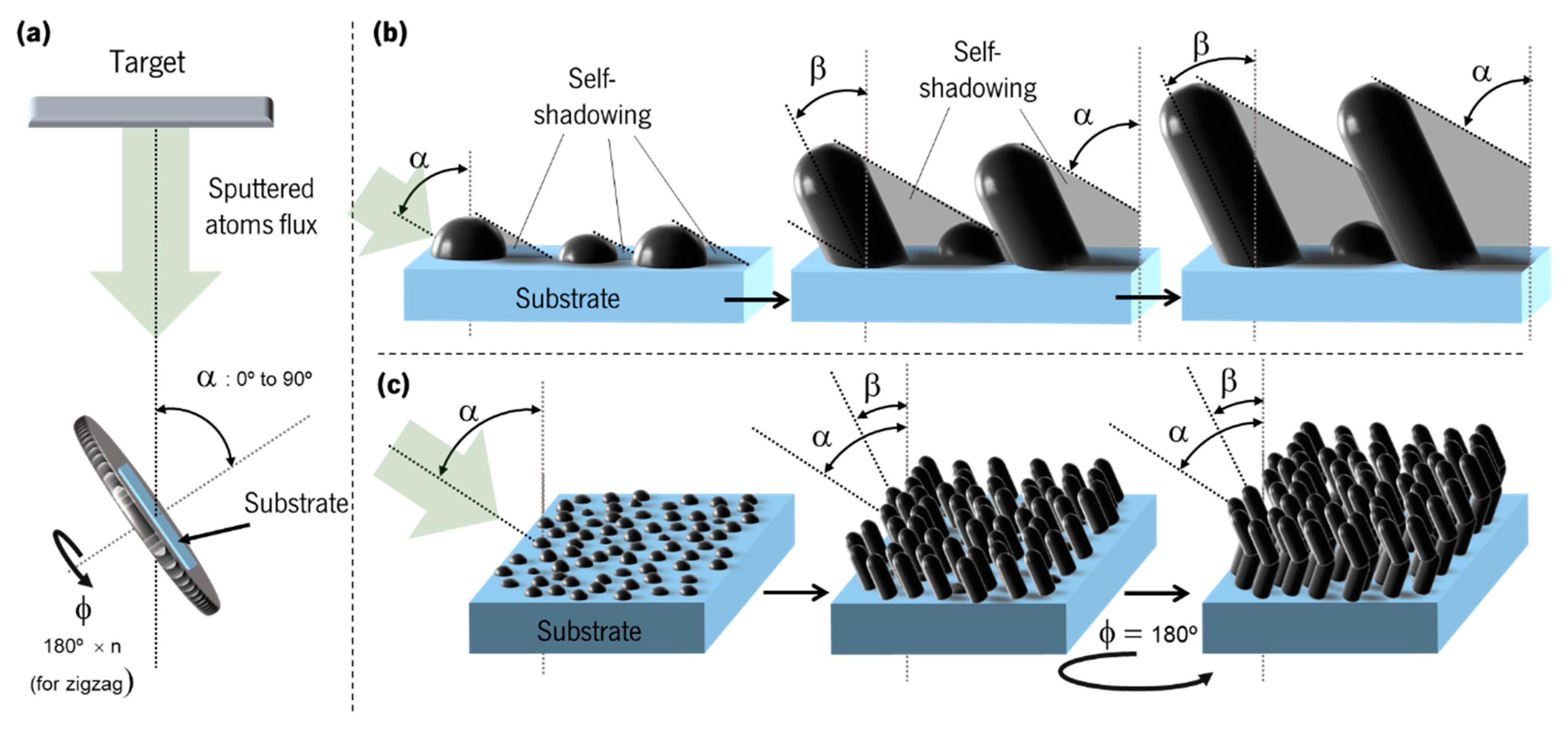
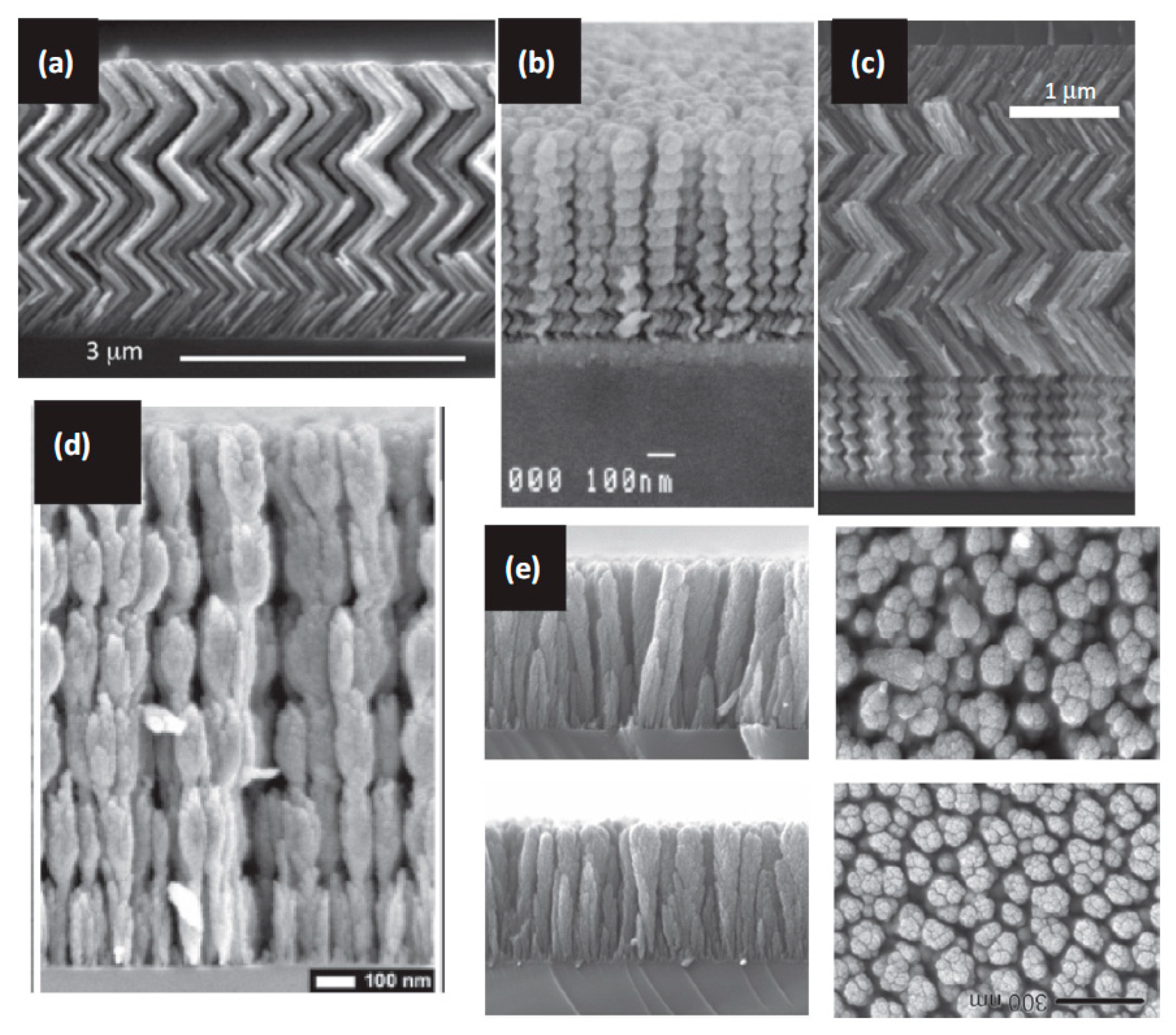
4.5. Glancing Angle Deposition (GLAD) to Tailor the Micro/Nano Structure

Nanostructured thin films can be achieved by glancing angle deposition (GLAD) in reactive magnetron sputtering. The fundamentals of GLAD, also known as oblique angle deposition (OAD), (Figure 15a) rely on the self-shadowing effect (Figure 15b) that appears just after the deposition of the first atoms, as long as the atom mobility remains low [181]. In conventional sputtering, the direction of the atom flux is perpendicular to the substrate (α = 0°), so the atoms condense on the nearest sites of nucleation or on the surrounding area to form the typical vertical columnar growth [141]. On the other hand, when the flux is not perpendicular to the surface (0° < α ≤ 90°), the atoms in the vapour phase condense on the substrate to form some nucleation sites, and, depending on several parameters (e.g., substrate condition and temperature or energy and nature of the atoms in the vapour phase), they may intercept the incoming atoms to produce a “shadow” on the substrate or on the material already deposited (Figure 15b). Due to this self-shadowing and although the atoms in the vapour phase reach the substrate at an angle α, the inclined columns grow at a lower angle β (Figure 15b). The effective column tilt angle β depends on several factors, namely material used, sputtered particle angle of incidence, substrate rotation speed, and gas pressure [182], and it can be roughly estimated, as a guideline, using Tait’s rule [183].
The self-shadowing process is also be responsible for producing more porous thin films, which, depending on the angle of incidence and on the material, can lead to nanostructured materials with only 10% of the bulk material’s density [184].
For an inclined columnar structure, only the angle of incidence (α) must be set, but by using another rotation axis φ (perpendicular to the substrate, Figure 15a). GLAD allows the development of layers with a zigzag structure (Figure 15c), spirals, isolated columns, and other configurations, only by combining different rotation speeds and protocols [185]. For example, to prepare zigzag structures, after an incidence angle (α) is selected, φ must be shifted by 180° at each half zigzag cycle, as depicted in Figure 15c. For spirals, an incidence angle (α) must be selected, and then φ must be changed slowly and continuously, and each time φ rotates 360° one spiral is produced. By changing the speed of rotation for φ angle, the shape of the spiral is changed, and if the speed is sufficiently high, instead of spirals, isolated columns may be produced. In this last configuration, the distance between each column will depend on the selected α angle [184] (see examples in Figure 16).
The discovery that the properties of thin films deposited by GLAD are different from conventional thin films was made at the end of the 1950s [186,187,188], and soon several theories developed for the explanation of the self-shadowing effect, the columnar growth according to β angle, and to account the different deposition rates, some of them already supported by computer simulations [181]. In the following decades, it was made clear by several authors that the induced morphological changes in the thin films could produce important anisotropy in the magnetic, electrical, mechanical, and optical properties [171,183,184,189].
Therefore, since the GLAD technique allows one to tailor even further the properties of most thin film systems, it can be of major interest in the fields of photonics, mechanics, catalysis, and biology. This involvement is mostly evident for metal and oxide coatings sputter deposited with inclined architectures [190,191]. However, for nanocomposite thin films containing noble metal nanoparticles, very few studies can be found about the relations between the possible achieved structures by GLAD and the resulting properties in terms of optical and other physical responses [170,192].

5. Tailoring the Sensitivity of LSPR-Based Sensors Using Simulation Models

5.1. Important Parameters Influencing the LSPR-Based Sensor Performance

According to the literature, so far the work carried out about surface plasmon resonance sensing has been mainly based on SPPs [16,49,193,194]. Yet, since surface plasmon effects can be much more prominent in nanoparticles than in continuous thin film layers [154,158,160,195,196,197], the nanoparticles can be exploited as intrinsic refractive index sensors [13], by monitoring shifts and curvature changes on the LSPR band (Figure 17a,b).
Optical sensors based on the LSPR phenomenon are recognized as advantageous candidates in the design of lab-on-chip platforms, providing a valid approach to achieve quantitative analysis while offering the possibility to be miniaturized [69,70,166,198,199,200,201].
For refractive index changes to produce a measurable shift in the resonance band, they must occur in a region of appreciable field intensity, namely, in a sensing volume contained within the plasmon’s electric field decay length ( L d ). Since the plasmon field decays exponentially with the distance from the nanoparticle, the effective sensing volume is typically limited to a length ranging from 10 to 30 nm, depending on the nanoparticle shape and size [52]. To quantify the sensitivity of a LSPR sensor to a refractive index change ( R I S , refractive index sensitivity, or just S, sensitivity) caused by an infinite surrounding environment (such as a gas), a simple phenomenological equation may be used— Δ P = R I S × Δ n s × ( 1 e d / L d ) —where Δ P is the variation of the measured parameter (which can be the LSPR resonance wavelength shift, Δ λ ), Δ n s is the refractive index difference between the two environments, d is the thickness of the layer, and L d the plasmon decay length.
From experimental and theoretical results in the literature, several parameters have been proposed as having an important influence in the sensitivity of plasmonic thin films. The proposed parameters, namely, the existence of sharp vertices in nanoparticles of exotic shapes (such as stars, pyramids, bipyramids, rings, crescents, and branches), the position of the LSPR resonance, or the full width at half height of the LSPR band, failed to give a complete explanation [173]. Meanwhile, it has been made clear that the aspect ratio (AR), independently of the shape (Figure 18a), is the most probable candidate parameter to tailor the sensitivity of plasmonic nanoparticles (Figure 18b) [202].

5.2. Optical Properties Modelling

The most widely used methods for modelling the optical properties of nanoparticles with sizes above 5 nm (where quantum mechanical calculations are not required) rely on solutions, numeric or via approximations, of the Maxwell equations, such as Mie theory-based codes, finite-difference time-domain (FDTD) approach, finite element method (FEM), and the discrete dipole approximation (DDA), among others [37,203,204,205,206].
Some of these methods use computationally intensive algorithms that are currently available to everyone thanks to the processing power of modern computers and clusters that run parallel computations in open access. NanoHUB [207] is an example of a user-friendly and web-based system, controlled by the Purdue University’s Network for Computational Nanotechnology and funded by the American National Science Foundation. It hosts a collection of simulation tools, which allow one to study light–matter interactions in different contexts. In particular, there are (i) “Nanosphere Optics Lab” [208] for an exact solution of Maxwell equations using the Mie theory for single spheres; (ii) “Extinction, Scattering and Absorption Efficiencies of Single and Multilayer Nanoparticles” [209] (Figure 19a), also using the Mie theory for single spheres, core-shell, and “nanomatryoshka” structures; (iii) “Molecular Foundry Photonics Toolkit” [210] (Figure 19b) for FDTD simulations; (iv) “MOOSE” [211,212] (Figure 19c), for advanced FEM simulations; and (v) “nanoDDSCAT+” [213] (Figure 19d) for DDA simulations with nanoparticles of arbitrary shapes.
Commercially available simulation tools include MATLAB (with incorporated Mie theory codes), Lumerical software (FDTD), and COMSOL Multiphysics (FEM), among others. Detailed comparisons of these and other methods may be found elsewhere [37,214,215,216,217,218], but the main decisions that one has to make in order to choose the best method are related to the following factors:
(i)
Nanoparticle shape (for instance, Mie codes and their extensions work only with high-symmetry shapes and the DDA uses a large amount of memory if the simulations use both large and very small shapes at the same time);
(ii)
Number of simulations to run (for instance, spectral calculations are time consuming for FDTD, FEM, and DDA);
(iii)
Type of output one is interested in, namely, only the local field intensity in the vicinity of a plasmonic structure, to find the most intense hot spots, or angular distribution of the scattered light intensity and polarization in the far field zone (for instance, COMSOL is ideal for the former but not so well-suited for the latter).
It is also necessary to consider that none of these tools can be used to directly calculate the response of a statistical ensemble of interacting nanoparticles, considering each of them explicitly (for instance, a composite layer containing arbitrarily shaped particles). For such a task one needs to apply either approximate methods known in the theory of disordered systems, which use either a self-consistent approach or a kind of perturbation theory [219,220,221,222] or solve numerically a system of equations that describes a relatively small, yet representative, set of interacting polarizable particles distributed in space according to some rules mimicking the real system, such as the coupled dipole equations (CDE), where each particle is approximated by a dipole [223].
Let us focus on the DDA approach, which is suitable for describing nanoparticles of arbitrary shape, both in the near-and far-field zone, and calculate the absorption and extinction cross sections. This is attractive in the context of modelling a sensing system because the plasmonic effect slightly perturbed by the presence of an analyte may be detected via a change in the position and shape of the LSPR band, but also through an altered polarization state of the resonantly scattered light. The DDA has been demonstrated to be one of the most powerful and flexible electrodynamic methods for computing the optical spectra of nanoparticles with an arbitrary geometry [37].
The idea was introduced by DeVoe, 1964 [224] who applied it to study the optical properties of molecular aggregates. DDA with retardation effects was presented in 1973 by Purcell and Pennypacker [225] to study the scattering and absorption of light of interstellar dust grains. They presented it as a method in which the continuum target is approximated by a finite array of polarizable points. These points acquire dipole moments due to the electric field of an incident wave. The dipoles interact with the neighbouring dipoles via their electric fields. These dipoles can be thought of as polarizable particles of simple geometries, such as spheres or spheroids (actually, it is very similar to the CDE approach for composite materials, mentioned above). The polarizability of the dipoles is related to properties of the material via its refractive index n s . The domain discretization is a very important first step. The method is expected to produce an acceptable response (almost a continuum target) on length scales much larger than the lattice spacing, d λ 0 (more rigorously, this criterion is 2 π n s d / λ 0 1 ). Roughness of a target can be mimicked by randomly removing some elements from the surface using a Monte Carlo sampling.
An obvious problem that appears for a target with a large size is that the number of small spheres necessary to describe the target is huge. Therefore, the memory/CPU requirements may be a problem (computational effort scales with the number of small spheres as N 3 and with memory needs scale as N 2 ) . LU decomposition, as stated by Draine and Flatau (1994) [226], is a solution for relatively small problems. However, for larger problems, iterative methods such as complex conjugate gradient-type methods might be used. This is the case of the method presented by Draine (1988) [227], where the iterative conjugate gradient algorithm (CGA) to find the dipole polarizations is described. When the number of particles N is large, this algorithm converges rapidly due to symmetries of the matrix. Since P has 3 N unknowns, this method converges in 3 N iterations, which is much faster than a direct method that must solve a linear system of equations [ A ] P = E , where [ A ] is a 3 N × 3 N dense matrix. Using fast-Fourier-transform (FFT) methods, as suggested by Goodman et al. (1991) [228], accelerates computations of scattering and absorption by particles of arbitrary shape using DDA and diminishes the CPU price that comes from a CGA method (multiplications matrix–vector, which are mostly convolutions).
As an illustration, we used the DDA method to estimate the sensitivity (RIS) of gold spheroids, with different AR, embedded in a TiO2 dielectric matrix. The spheroids were exposed to environments with different refractive indices and two sets of simulations of the optical properties were undertaken. The simulations presented in the next section were carried out using the already mentioned nanoDDSCAT+ tool [213] (Figure 19d), which is powered by Draine and Flatau’s DDSCAT (v7.3) code [226], and uses DDA for calculating scattering and absorption (hence extinction) of light by particles with arbitrary shapes.

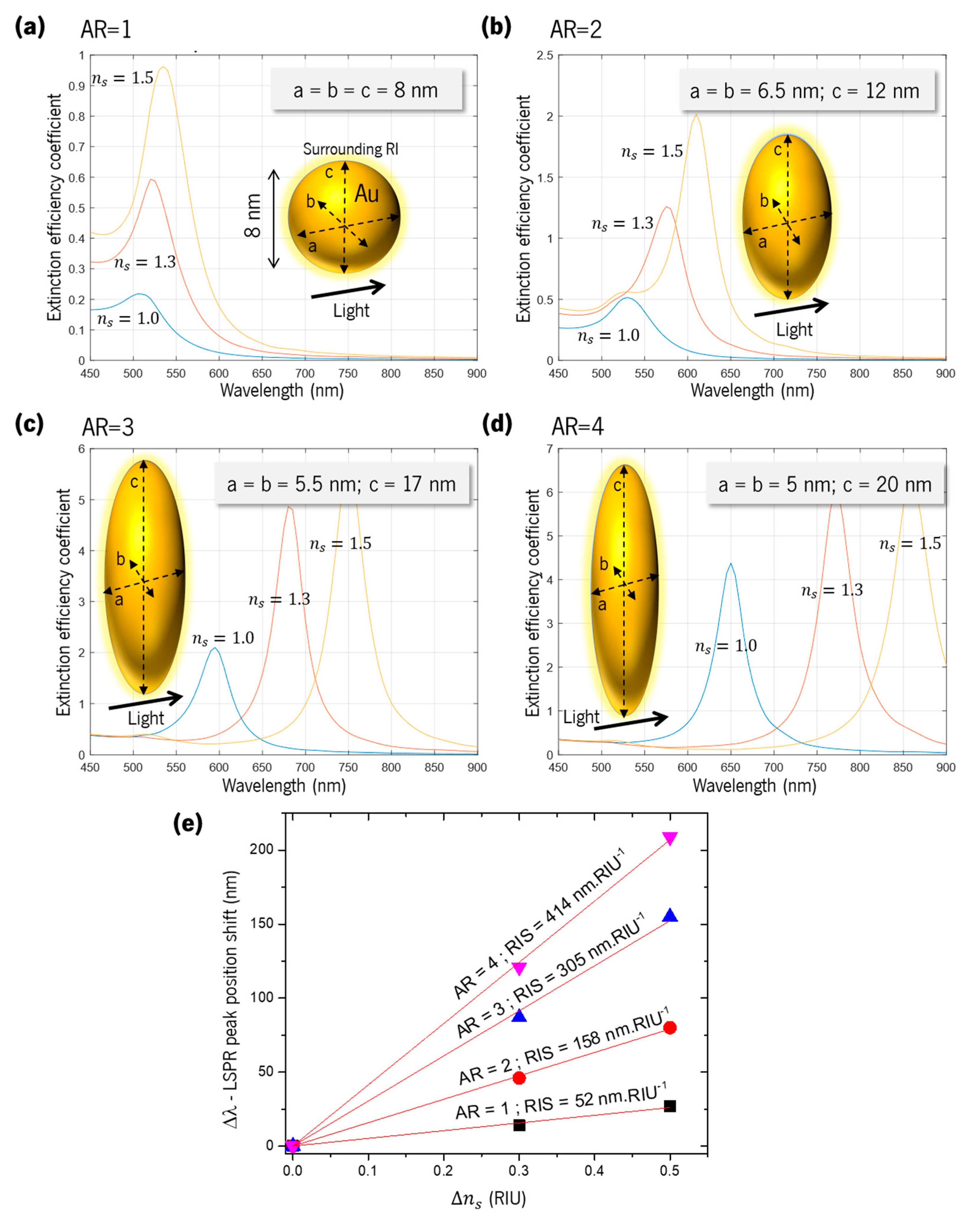
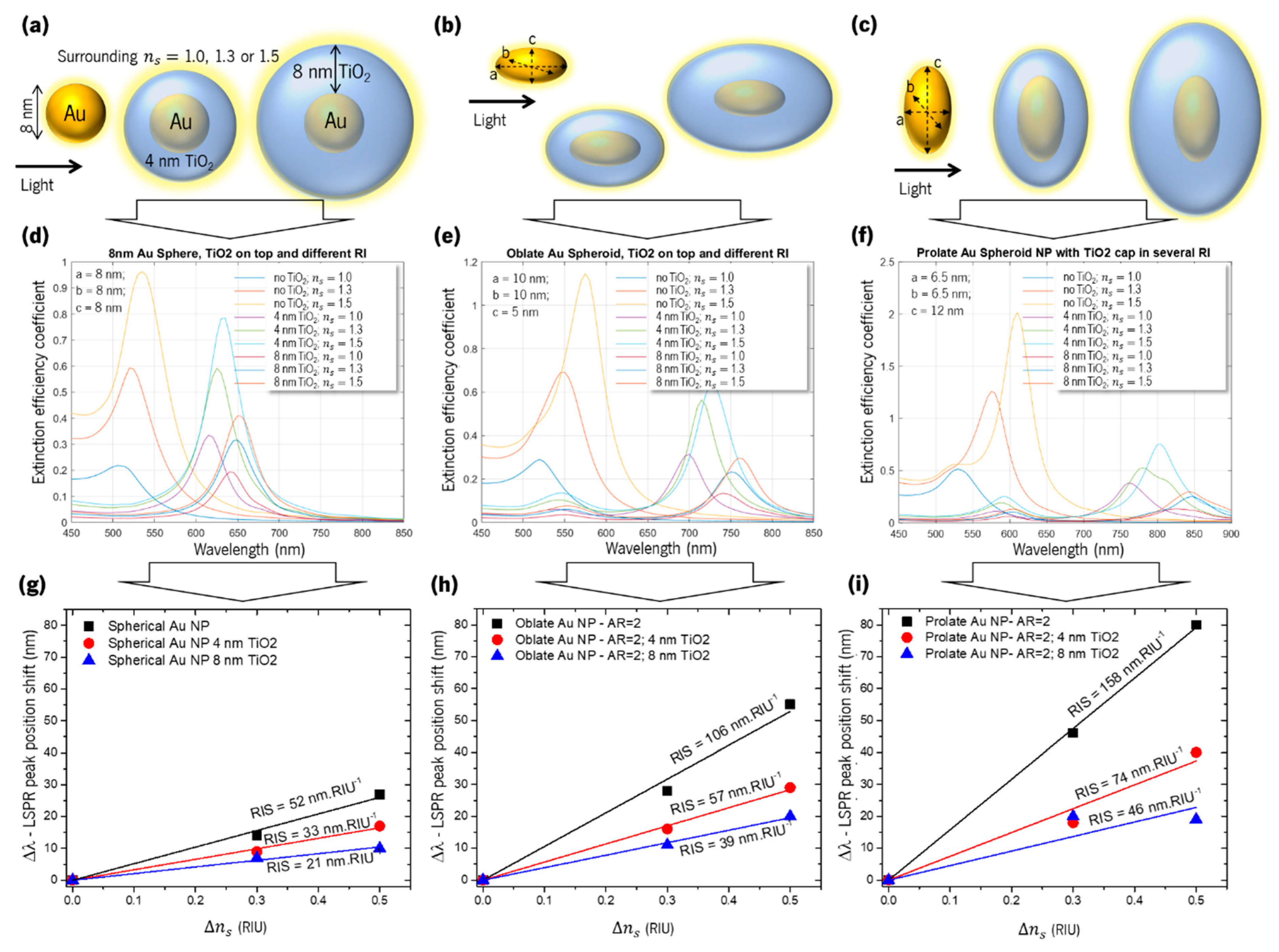
5.3. Sensitivity of a Spheroid Au Nanoparticle Embedded in TiO2

In the first set of simulations (Figure 20), the RIS of nanoparticles with different aspect ratios was estimated. In the DDA simulations, the nanoparticles had an effective radius of 8 nm, which represents the radius of a sphere having a volume equal to that of the nanoparticle [229]. The principal settings used in the simulations follow:
(i)
Unpolarized light;
(ii)
Four dipoles per nm;
(iii)
Au dielectric function from Johnson and Christy [230];
(iv)
TiO2 dielectric constant (ε = 6.8121, or n s = 2.61);
(v)
Surrounding external refractive index set either to 1.0, 1.3, or 1.5, as a “semi-infinite” layer;
(vi)
A wavelength range from 450 to 900 nm with a 5 nm step.
Considering the size of the nanoparticles used for the simulations, the scattering efficiency coefficient is negligible when compared to the absorption efficiency coefficient (up to three orders of magnitude) [229,231]. Thus, the extinction efficiency coefficient (the sum of the two previous) presented in the results is roughly the same as the absorption efficiency coefficient.
Indeed, it is obvious from Figure 20a–d, that for spheroids with higher AR when the surrounding refractive index increases (from 1.0 to 1.5), the shift of the extinction efficiency coefficient is also increasing from 26 nm for AR = 1 and up to 207 nm for AR = 4. Then, by plotting Δ λ against Δ n s (Figure 20e), the RIS can be estimated: 52 nm/RIU, 158 nm/RIU, 305 nm/RIU, and 414 nm/RIU, for AR of 1, 2, 3, and 4, respectively, thus giving an overall eight-fold improvement. These results are in line with the literature data collection depicted in Figure 18b.
From these simulations it looks obvious that the enhanced sensitivity comes from the longitudinal vibration modes of the LSPs, since their intensity seems to be much higher than that of the transverse modes [232]. Therefore, it is advantageous to have nanoparticles with higher aspect ratio since their sensitivity is much higher than spherical shapes. This property might be fine-tuned with the GLAD technique [97].
In the second set of simulations (Figure 21), the effect of a TiO2 cap layer covering an Au sphere (AR = 1, Figure 21a), an oblate spheroid (AR = 2, Figure 21b), and a prolate spheroid (AR = 2, Figure 21c) were studied. From Figure 21d–f, it can be concluded that by adding a 4 nm and then an 8 nm TiO2 layer, the intensity of the extinction efficiency coefficient is gradually diminished. Similarly, the sensitivity (RIS) estimated with the against Δ n s plots in Figure 21g–i, also decreases with increasing thickness of the surrounding TiO2 layer.
It means that when the Au nanoparticles are grown within an oxide matrix, the sensitivity of the optical LSPR response of the Au nanoparticles is impaired. This effect is due to the plasmon decay length that follows an exponential decrease from the surface of the nanoparticle, as mentioned before. To overcome this hurdle, the surface of the films can be etched to eliminate superficial oxide layers, thus diminishing the distance between the nanoparticles and the molecules to detect, thereby improving the sensitivity. Furthermore, in agreement with the previous set of simulations, the aspect ratio of the nanoparticles also plays an important role when the nanoparticles are covered by the dielectric matrix. As seen in Figure 21g–i, the sensitivity is improved with the AR increase even if the TiO2 capping layer is surrounding the nanoparticle. For instance, prolate or oblate spheroids with an AR of 2 and a 4 nm TiO2 capping layer (Figure 21h,i) have a higher sensitivity (57 nm/RIU and 74 nm/RIU) than a gold sphere without a TiO2 capping layer (52 nm/RIU, Figure 21g).
These sensitivity simulation results, summarized in Table 3, are the consequence of an interaction of light with single nanoparticles with a well-described shape and size. Under these circumstances, the extinction spectrum redshifts when the surrounding refractive index increases, thus giving the foundation of optical LSPR sensing for refractive index changes. Unfortunately, even with well-defined arrays of Ag or Au nanoparticles, a continuous distribution of their size and aspect ratio is obtained [233]. Furthermore, since the nanoparticles must be supported by a substrate, the sensing volume also changes. This must be kept in mind when analysing LSPR sensitivity results from an ensemble of nanoparticles, since the expected redshift of the LSPR band can result in an overall blueshift.

6. Technoeconomic Challenges

The technologies behind the development of this new generation of nanoplasmonic thin film sensors are vacuum deposition techniques, which are recognized as clean and environmentally sound technologies, since no dangerous byproducts or waste are produced.
Although the initial cost of vacuum deposition techniques may be somewhat high when it comes to industrial upscaling, the production of these thin film sensors by magnetron sputtering, an efficient physical vapour deposition (PVD) technique, reveals it to be an economically viable process. To produce one thin film sensor (8 × 8 mm2) in a R&D vacuum deposition chamber (where approximately 300 thin film sensors can be deposited simultaneously), the estimated production cost is around EUR 0.20. This value also includes the thermal treatment required to promote the growth of nanoparticles (see Section 4.3) and plasma treatments to enhance the sensitivity (see Section 4.4).
If the thermal treatment and the working temperature do not exceed 450 °C [168], one may consider an inexpensive substrate, such as glass. This type of substrate may increase the final cost by 3% to 5%, which is a marginal difference. Nevertheless, if a temperature above 450 °C is needed [169,234], more expensive substrates are required. For example, if a fused silica substrate is used, the final cost of the thin film sensor can increase up to EUR 0.75.
Regarding the use of the GLAD technique, the substrate space limitation inside the vacuum system makes it an expensive technique, since only around 30 thin film sensors can be deposited in a similar R&D system, increasing their production cost by a factor of 10. Moreover, upscaling the production to an industrial system is not revealed to be a simple task [235], and further research is needed.

7. Conclusions and Outlook

In this article, a review is presented on gas sensors based on the localized surface plasmon resonance (LSPR) phenomenon, focused on earliest and modern applications of plasmonic nanoparticles. Furthermore, the synthesis of nanoparticle-embedded nanostructured oxide/nitride thin films and experimental strategies to enhance their sensitivity are discussed, complemented by simulation and modelling results.
According to the historical and technological overview on conductometric and optical gas sensors (electronic-nose systems), it is foreseen that in the forthcoming years nanomaterial-based sensors will play an important role in several industrial sectors, leading to growth in a worldwide market. Among several applications that plasmonic nanoparticles can offer, LSPR sensing platforms have been the focus of much research due to the straightforward detection mechanism and experimental setups needed.
We show that metal oxides can be robust materials to host nanoparticles and boost their sensing capabilities. The preparation method of nanocomposite plasmonic thin films highlighted in this paper consists of reactive magnetron sputtering deposition, followed by thermal annealing, while glancing angle deposition (GLAD) and low-pressure plasma treatment are presented as important techniques to tailor the film nanostructures and hence to improve their optical sensing responses. Of course, it does not mean that chemically synthesized nanoparticles are not promising for sensing applications [82,103].
Finally, several simulation methods are described, and the optical LSPR sensitivity of gold nanoparticles with different shapes and sensing volumes estimated using discrete dipole approximation (DDA) models. The simulations confirmed that the enhanced sensitivity in spheroidal nanoparticles comes from the longitudinal vibration modes of the localized surface plasmons that arise when their aspect ratio increases. When Au nanoparticles are embedded in an oxide matrix, their sensitivity is reduced. From these simulations, it becomes clear that an oxide matrix can be used to mechanically protect the nanoparticles, and still allowing them to maintain their sensing capabilities. Furthermore, the sensing capabilities of these embedded nanoparticles can be optimized by adjusting their aspect ratios, and physically erode the excess oxide layer around them. To further investigate the sensitivity of nanoparticles in real systems, simulation models using the theory of disordered systems, with a self-consistent approach or a kind of perturbation theory must be used, since even the most powerful modern computers do not allow for modelling large systems that include many nanoparticles by direct solution of discretized Maxwell equations or even with approximations such as DDA.

Author Contributions

Conceptualization, M.S.R., J.B., and F.V.; methodology, M.S.R., J.B., C.L., and R.M.S.P.; software, M.S.R. and R.M.S.P.; validation, J.B., M.I.V., and F.V.; formal analysis, M.S.R., J.B., and R.M.S.P.; investigation, M.S.R., J.B., C.L., and R.M.S.P.; resources, J.B. and F.V.; data curation, M.S.R., R.M.S.P., and J.B.; writing—original draft preparation, M.S.R., J.B., and C.L.; writing—review and editing, M.S.R., J.B., C.L, R.M.S.P., M.I.V., and F.V.; visualization, M.S.R., J.B., C.L., M.I.V., and F.V.; supervision, J.B. and F.V.; project administration, J.B. and F.V.; funding acquisition, J.B. and F.V. All authors have read and agreed to the published version of the manuscript.

Funding

This research was funded by the Portuguese Foundation for Science and Technology (FCT) in the framework of the Strategic Funding UIDB/04650/2020; and by the project NANO4BIO POCI-01-0145-FEDER-032299, with FCT reference PTDC/FISMAC/32299/2017. Marco S. Rodrigues acknowledges FCT for his PhD Scholarship, SFRH/BD/118684/2016.

Conflicts of Interest

The authors declare no conflict of interest.

References

  1. Arshak, K.; Moore, E.; Lyons, G.M.; Harris, J.; Clifford, S. A review of gas sensors employed in electronic nose applications. Sens. Rev. 2004, 24, 181–198. [Google Scholar] [CrossRef] [Green Version]
  2. Lafreniere, D.; Mann, N. Anosmia: Loss of Smell in the Elderly. Otolaryngol. Clin. N. Am. 2009, 42, 123–131. [Google Scholar] [CrossRef]
  3. Brattain, W.H.; Bardeen, J. Surface properties of germanium. Bell Syst. Tech. J. 1953, 32, 1–41. [Google Scholar] [CrossRef]
  4. Heiland, G. Zum Einfluß von adsorbiertem Sauerstoff auf die elektrische Leitfähigkeit von Zinkoxydkristallen. Z. Für Phys. 1954, 138, 459–464. [Google Scholar] [CrossRef]
  5. Wilkens, W.F.; Hartman, J.D. An Electronic Analog for the Olfactory Processesa. J. Food Sci. 1964, 29, 372–378. [Google Scholar] [CrossRef]
  6. Neri, G. First Fifty Years of Chemoresistive Gas Sensors. Chemosensors 2015, 3, 1–20. [Google Scholar] [CrossRef]
  7. Göpel, W. Solid-state chemical sensors: Atomistic models and research trends. Sens. Actuators 1989, 16, 167–193. [Google Scholar] [CrossRef]
  8. Xu, K.; Fu, C.; Gao, Z.; Wei, F.; Ying, Y.; Xu, C.; Fu, G. Nanomaterial-based gas sensors: A review. Instrum. Sci. Technol. 2018, 46, 115–145. [Google Scholar] [CrossRef]
  9. Schierbaum, K.D.; Vaihinger, S.; Göpel, W.; van den Vlekkert, H.H.; Kloeck, B.; de Rooij, N.F. Prototype structure for systematic investigations of thin-film gas sensors. Sens. Actuators B Chem. 1990, 1, 171–175. [Google Scholar] [CrossRef]
  10. Pinto, R.M.R.; Brito, P.; Chu, V.; Conde, J.P. Thin-Film Silicon MEMS for Dynamic Mass Sensing in Vacuum and Air: Phase Noise, Allan Deviation, Mass Sensitivity and Limits of Detection. J. Microelectromech. Syst. 2019, 28, 390–400. [Google Scholar] [CrossRef]
  11. Behzadi pour, G.; Fekri aval, L. Highly sensitive work function hydrogen gas sensor based on PdNPs/SiO2/Si structure at room temperature. Results Phys. 2017, 7, 1993–1999. [Google Scholar] [CrossRef]
  12. Soares, L.; Csáki, A.; Jatschka, J.; Fritzsche, W.; Flores, O.; Franco, R.; Pereira, E. Localized surface plasmon resonance (LSPR) biosensing using gold nanotriangles: Detection of DNA hybridization events at room temperature. Analyst 2014, 139, 4964–4973. [Google Scholar] [CrossRef]
  13. Bingham, J.M.; Anker, J.N.; Kreno, L.E.; Van Duyne, R.P. Gas Sensing with High-Resolution Localized Surface Plasmon Resonance Spectroscopy. J. Am. Chem. Soc. 2010, 132, 17358–17359. [Google Scholar] [CrossRef] [Green Version]
  14. Chang, C.-Y.; Lin, H.-T.; Lai, M.-S.; Shieh, T.-Y.; Peng, C.-C.; Shih, M.-H.; Tung, Y.-C. Flexible Localized Surface Plasmon Resonance Sensor with Metal–Insulator–Metal Nanodisks on PDMS Substrate. Sci. Rep. 2018, 8, 11812. [Google Scholar] [CrossRef]
  15. Farooq, S.; Neves, W.W.; Pandoli, O.; Del Rosso, T.; de Lima, L.M.; Dutra, R.F.; Araujo, R.E. de Engineering a plasmonic sensing platform for Candida albicans antigen identification. J. Nanophotonics 2018, 12, 1–10. [Google Scholar] [CrossRef]
  16. Koutsioubas, A.G.; Spiliopoulos, N.; Anastassopoulos, D.L.; Vradis, A.A.; Priftis, G.D. On the implementation of nano-structured materials in surface plasmon resonance sensors. Mater. Sci. Eng. B 2009, 165, 270–273. [Google Scholar] [CrossRef]
  17. Yang, Z.; Sassa, F.; Hayashi, K. A robot equipped with a high-speed LSPR gas sensor module for collecting spatial odor information from on-ground invisible odor sources. ACS Sens. 2018, 3, 1174–1181. [Google Scholar] [CrossRef] [PubMed]
  18. Oh, S.Y.; Heo, N.S.; Bajpai, V.K.; Jang, S.-C.; Ok, G.; Cho, Y.; Huh, Y.S. Development of a Cuvette-Based LSPR Sensor Chip Using a Plasmonically Active Transparent Strip. Front. Bioeng. Biotechnol. 2019, 7, 299. [Google Scholar] [CrossRef] [PubMed]
  19. Castillero, P.; Roales, J.; Lopes-Costa, T.; Sánchez-Valencia, J.; Barranco, A.; González-Elipe, A.; Pedrosa, J. Optical Gas Sensing of Ammonia and Amines Based on Protonated Porphyrin/TiO2 Composite Thin Films. Sensors 2016, 17, 24. [Google Scholar] [CrossRef] [PubMed] [Green Version]
  20. Pereira-Silva, P.; Costa-Barbosa, A.; Costa, D.; Rodrigues, M.S.; Carvalho, P.; Borges, J.; Vaz, F.; Sampaio, P. Antifungal activity of ZnO thin films prepared by glancing angle deposition. Thin Solid Film. 2019, 687, 137461. [Google Scholar] [CrossRef]
  21. Proença, M.; Rodrigues, M.S.; Borges, J.; Vaz, F. Gas Sensing with Nanoplasmonic Thin Films Composed of Nanoparticles (Au, Ag) Dispersed in a CuO Matrix. Coatings 2019, 9, 337. [Google Scholar] [CrossRef] [Green Version]
  22. Sabri, N.; Aljunid, S.A.; Salim, M.S.; Ahmad, R.B.; Kamaruddin, R. Toward Optical Sensors: Review and Applications. J. Phys. Conf. Ser. 2013, 423, 12064. [Google Scholar] [CrossRef]
  23. Ng, S.M. 12—Carbon Dots as Optical Nanoprobes for Biosensors. In Micro and Nano Technologies; Gopinath, S.C.B., Lakshmipriya, T.B.T.-N., Eds.; Elsevier: Amsterdam, The Netherlands, 2019; pp. 269–300. ISBN 978-0-12-813900-4. [Google Scholar]
  24. Chemical Sensors Market Forecast, Trend Analysis & Competition Tracking—Global Market Insights 2018 to 2028; Fact.MR: Dublin, Ireland, 2020.
  25. Chemical Sensors Market: Global Demand Analysis & Opportunity Outlook 2024; Research Nester: New York, NY, USA, 2020.
  26. Gas Sensors Market by Gas Type (Oxygen, Carbon Monoxide, Carbon Dioxide, Ammonia, Chlorine, Hydrogen Sulfide, Nitrogen Oxide, Volatile Organic Compounds, Hydrocarbons), Technology, Application, Geography—Global Forecast 2024; MarketsandMarkets: Northbrook, IL, USA, 2021.
  27. Olson, K.R. Carbon monoxide poisoning: Mechanisms, presentation, and controversies in management. J. Emerg. Med. 1984, 1, 233–243. [Google Scholar] [CrossRef]
  28. Rose, J.J.; Wang, L.; Xu, Q.; McTiernan, C.F.; Shiva, S.; Tejero, J.; Gladwin, M.T. Carbon Monoxide Poisoning: Pathogenesis, Management, and Future Directions of Therapy. Am. J. Respir. Crit. Care Med. 2016, 195, 596–606. [Google Scholar] [CrossRef] [PubMed]
  29. Stone, B.L. Chapter 38—Hypoxemia; Zaoutis, L.B., Ed.; Mosby: Philadelphia, PA, USA, 2007; pp. 181–189. ISBN 978-0-323-03004-5. [Google Scholar]
  30. Eckhoff, R.K. Explosion Hazards in the Process Industries, 2nd ed.; Elsevier: Amsterdam, The Netherlands, 2016; ISBN 9780128032732. [Google Scholar]
  31. Stockman, M.I. Nanoplasmonics: The physics behind the applications. Phys. Today 2011, 64, 39–44. [Google Scholar] [CrossRef] [Green Version]
  32. Barber, D.J.; Freestone, I.C. An investigation of the origin of the colour of the lycurgus cup by analytical transmission electron microscopy. Archaeometry 1990, 32, 33–45. [Google Scholar] [CrossRef]
  33. Dekker, F.; Kool, L.; Bunschoten, A.; Velders, A.H.; Saggiomo, V. Syntheses of gold and silver dichroic nanoparticles; looking at the Lycurgus cup colors. Chem. Teach. Int. 2019. [Google Scholar] [CrossRef]
  34. Freestone, I.; Meeks, N.; Sax, M.; Higgitt, C. The Lycurgus Cup—A Roman nanotechnology. Gold Bull. 2007, 40, 270–277. [Google Scholar] [CrossRef] [Green Version]
  35. Kool, L.; Bunschoten, A.; Velders, A.H.; Saggiomo, V. Gold nanoparticles embedded in a polymer as a 3D-printable dichroic nanocomposite material. Beilstein J. Nanotechnol. 2019, 10, 442–447. [Google Scholar] [CrossRef]
  36. Borges, J.; Rodrigues, M.S.; Kubart, T.; Kumar, S.; Leifer, K.; Evaristo, M.; Cavaleiro, A.; Apreutesei, M.; Pereira, R.M.S.; Vasilevskiy, M.I.; et al. Thin films composed of gold nanoparticles dispersed in a dielectric matrix: The influence of the host matrix on the optical and mechanical responses. Thin Solid Film. 2015, 596, 8–17. [Google Scholar] [CrossRef]
  37. Gonçalves, M.R. Plasmonic nanoparticles: Fabrication, simulation and experiments. J. Phys. D Appl. Phys. 2014, 47, 213001. [Google Scholar] [CrossRef]
  38. Bohren, C.F.; Huffman, D.R. Absorption and Scattering of Light by Small Particles; Wiley Online Books; Wiley: New York, NY, USA, 1998; ISBN 9780471293408. [Google Scholar]
  39. Landau, L.D.; Pitaevskii, L.P.; Lifshitz, E.M. Electrodynamics of Continuous Media, 2nd ed.; Butterworth-Heinemann: Oxford, UK, 1984; ISBN 9780080570600. [Google Scholar]
  40. Pettine, J.; Choo, P.; Medeghini, F.; Odom, T.W.; Nesbitt, D.J. Plasmonic nanostar photocathodes for optically-controlled directional currents. Nat. Commun. 2020, 11, 1367. [Google Scholar] [CrossRef] [PubMed] [Green Version]
  41. Pitarke, J.M.; Silkin, V.M.; Chulkov, E.V.; Echenique, P.M. Theory of surface plasmons and surface-plasmon polaritons. Rep. Prog. Phys. 2007, 70, 1–87. [Google Scholar] [CrossRef]
  42. Bludov, Y.U.V.; Ferreira, A.; Peres, N.M.R.; Vasilevskiy, M.I. A primer on surface plasmon-polaritons in graphene. Int. J. Mod. Phys. B 2013, 27, 1341001. [Google Scholar] [CrossRef] [Green Version]
  43. McQuillan, A.J. The discovery of surface-enhanced Raman scattering. Notes Rec. R. Soc. 2009, 63, 105–109. [Google Scholar] [CrossRef]
  44. Pereira, R.M.S.; Borges, J.; Peres, F.C.R.; Pereira, P.A.S.; Smirnov, G.V.; Vaz, F.; Cavaleiro, A.; Vasilevskiy, M.I. Effect of clustering on the surface plasmon band in thin films of metallic nanoparticles. J. Nanophotonics 2015, 9, 093796. [Google Scholar] [CrossRef]
  45. Toudert, J.; Simonot, L.; Camelio, S.; Babonneau, D. Advanced optical effective medium modeling for a single layer of polydisperse ellipsoidal nanoparticles embedded in a homogeneous dielectric medium: Surface plasmon resonances. Phys. Rev. B 2012, 86, 45415. [Google Scholar] [CrossRef] [Green Version]
  46. Scholl, J.A.; Koh, A.L.; Dionne, J.A. Quantum plasmon resonances of individual metallic nanoparticles. Nature 2012, 483, 421–427. [Google Scholar] [CrossRef]
  47. Stockman, M.I.; Kneipp, K.; Bozhevolnyi, S.I.; Saha, S.; Dutta, A.; Ndukaife, J.; Kinsey, N.; Reddy, H.; Guler, U.; Shalaev, V.M.; et al. Roadmap on plasmonics. J. Opt. 2018, 20, 043001. [Google Scholar] [CrossRef] [Green Version]
  48. Giannini, V.; Fernández-Domínguez, A.I.; Heck, S.C.; Maier, S.A. Plasmonic Nanoantennas: Fundamentals and Their Use in Controlling the Radiative Properties of Nanoemitters. Chem. Rev. 2011, 111, 3888–3912. [Google Scholar] [CrossRef]
  49. Maier, S.A. Plasmonics: Fundamentals and Applications; Springer: New York, NY, USA, 2007; ISBN 978-0-387-37825-1. [Google Scholar]
  50. Kahl, P.; Podbiel, D.; Schneider, C.; Makris, A.; Sindermann, S.; Witt, C.; Kilbane, D.; Hoegen, M.H.; Aeschlimann, M.; zu Heringdorf, F.M. Direct Observation of Surface Plasmon Polariton Propagation and Interference by Time-Resolved Imaging in Normal-Incidence Two Photon Photoemission Microscopy. Plasmonics 2018, 13, 239–246. [Google Scholar] [CrossRef]
  51. Willets, K.A.; Van Duyne, R.P. Localized Surface Plasmon Resonance Spectroscopy and Sensing. Annu. Rev. Phys. Chem. 2007, 58, 267–297. [Google Scholar] [CrossRef] [Green Version]
  52. Kedem, O.; Vaskevich, A.; Rubinstein, I. Critical Issues in Localized Plasmon Sensing. J. Phys. Chem. C 2014, 118, 8227–8244. [Google Scholar] [CrossRef]
  53. Li, D.-B.; Sun, X.-J.; Jia, Y.-P.; Stockman, M.I.; Paudel, H.P.; Song, H.; Jiang, H.; Li, Z.-M. Direct observation of localized surface plasmon field enhancement by Kelvin probe force microscopy. Light Sci. Appl. 2017, 6, e17038. [Google Scholar] [CrossRef] [PubMed]
  54. Svedendahl, M.; Chen, S.; Käll, M. An Introduction to Plasmonic Refractive Index Sensing BT—Nanoplasmonic Sensors; Dmitriev, A., Ed.; Springer: New York, NY, USA, 2012; pp. 1–26. ISBN 978-1-4614-3933-2. [Google Scholar]
  55. Vasilevskiy, M.I. Effective Dielectric Response of Composites Containing Uniaxial Inclusions. Phys. Status Solidi 2000, 219, 197–204. [Google Scholar] [CrossRef]
  56. Baida, H.; Billaud, P.; Marhaba, S.; Christofilos, D.; Cottancin, E.; Crut, A.; Lermé, J.; Maioli, P.; Pellarin, M.; Broyer, M.; et al. Quantitative Determination of the Size Dependence of Surface Plasmon Resonance Damping in Single Ag@SiO2 Nanoparticles. Nano Lett. 2009, 9, 3463–3469. [Google Scholar] [CrossRef] [PubMed]
  57. Kristensen, A.; Yang, J.K.W.; Bozhevolnyi, S.I.; Link, S.; Nordlander, P.; Halas, N.J.; Mortensen, N.A. Plasmonic colour generation. Nat. Rev. Mater. 2016, 2, 16088. [Google Scholar] [CrossRef]
  58. Adnan, N.N.M.; Cheng, Y.Y.; Ong, N.M.N.; Kamaruddin, T.T.; Rozlan, E.; Schmidt, T.W.; Duong, H.T.T.; Boyer, C. Effect of gold nanoparticle shapes for phototherapy and drug delivery. Polym. Chem. 2016, 7, 2888–2903. [Google Scholar] [CrossRef]
  59. Zhang, J.; Song, F.; Lin, S.; Liu, S.; Liu, Y. Tunable fluorescence lifetime of Eu-PMMA films with plasmonic nanostructures for multiplexing. Opt. Express 2016, 24, 8228–8236. [Google Scholar] [CrossRef]
  60. Song, M.; Wang, D.; Peana, S.; Choudhury, S.; Nyga, P.; Kudyshev, Z.A.; Yu, H.; Boltasseva, A.; Shalaev, V.M.; Kildishev, A. V Colors with plasmonic nanostructures: A full-spectrum review. Appl. Phys. Rev. 2019, 6, 41308. [Google Scholar] [CrossRef] [Green Version]
  61. Notarianni, M.; Vernon, K.; Chou, A.; Aljada, M.; Liu, J.; Motta, N. Plasmonic effect of gold nanoparticles in organic solar cells. Sol. Energy 2014, 106, 23–37. [Google Scholar] [CrossRef] [Green Version]
  62. Pluchery, O.; Remita, H.; Schaming, D. Demonstrative experiments about gold nanoparticles and nanofilms: An introduction to nanoscience. Gold Bull. 2013, 46, 319–327. [Google Scholar] [CrossRef] [Green Version]
  63. Anker, J.N.; Hall, W.P.; Lyandres, O.; Shah, N.C.; Zhao, J.; Van Duyne, R.P. Biosensing with plasmonic nanosensors. Nat. Mater. 2008, 7, 442–453. [Google Scholar] [CrossRef] [PubMed]
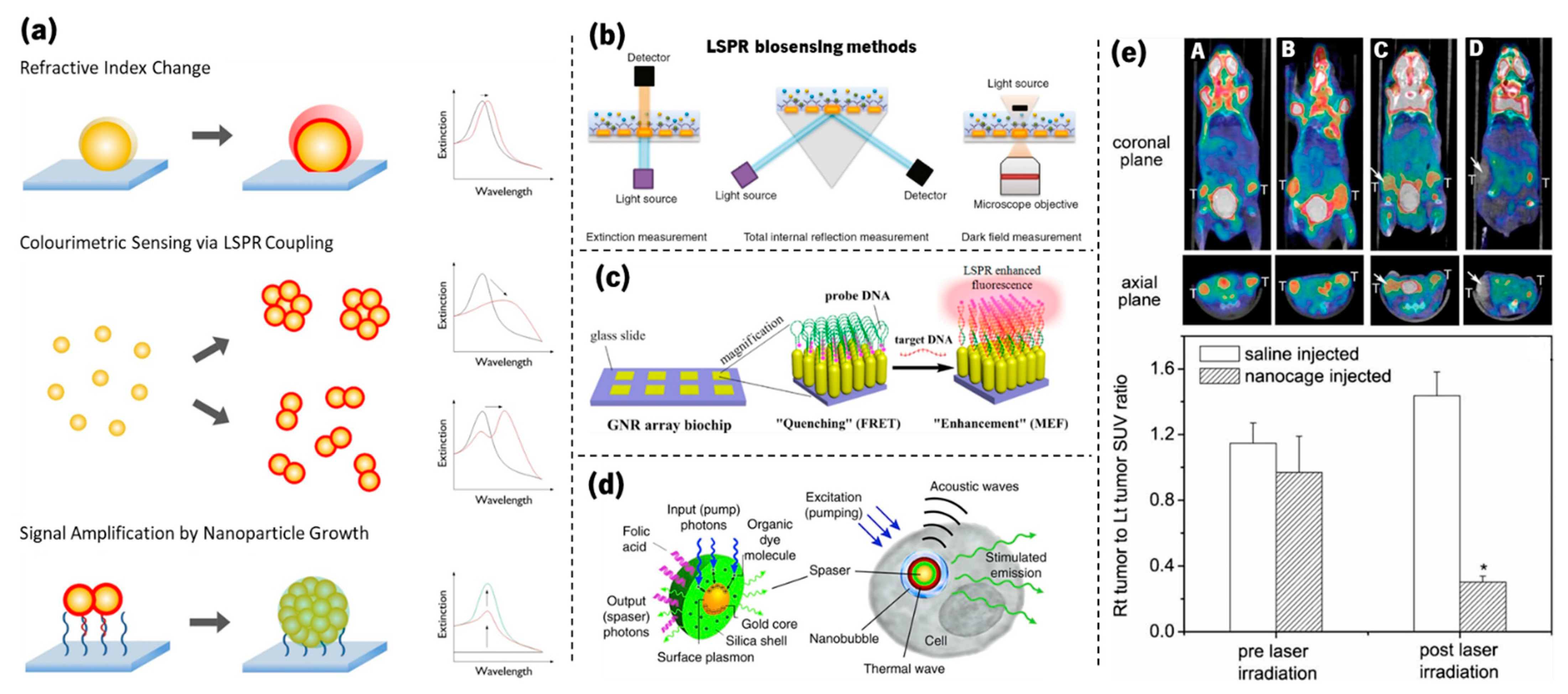
  64. Guo, L.; Jackman, J.A.; Yang, H.H.; Chen, P.; Cho, N.J.; Kim, D.H. Strategies for enhancing the sensitivity of plasmonic nanosensors. Nano Today 2015, 10, 213–239. [Google Scholar] [CrossRef] [Green Version]
  65. Kazuma, E.; Tatsuma, T. Localized surface plasmon resonance sensors based on wavelength-tunable spectral dips. Nanoscale 2014, 6, 2397–2405. [Google Scholar] [CrossRef] [PubMed] [Green Version]
  66. Sannomiya, T.; Vörös, J. Single plasmonic nanoparticles for biosensing. Trends Biotechnol. 2011, 29, 343–351. [Google Scholar] [CrossRef]
  67. Piliarik, M.; Šípová, H.; Kvasnička, P.; Galler, N.; Krenn, J.R.; Homola, J. High-resolution biosensor based on localized surface plasmons. Opt. Express 2012, 20, 672. [Google Scholar] [CrossRef]
  68. Soler, M.; Huertas, C.S.; Lechuga, L.M. Label-free plasmonic biosensors for point-of-care diagnostics: A review. Expert Rev. Mol. Diagn. 2019, 19, 71–81. [Google Scholar] [CrossRef] [PubMed]
  69. Cappi, G.; Spiga, F.M.; Moncada, Y.; Ferretti, A.; Beyeler, M.; Bianchessi, M.; Decosterd, L.; Buclin, T.; Guiducci, C. Label-Free Detection of Tobramycin in Serum by Transmission-Localized Surface Plasmon Resonance. Anal. Chem. 2015, 87, 5278–5285. [Google Scholar] [CrossRef]
  70. Lopez, G.A.; Estevez, M.C.; Soler, M.; Lechuga, L.M. Recent advances in nanoplasmonic biosensors: Applications and lab-on-a-chip integration. Nanophotonics 2017, 6, 123–136. [Google Scholar] [CrossRef]
  71. Rodrigues, M.S.; Pereira, R.M.S.; Vasilevskiy, M.I.; Borges, J.; Vaz, F. NANOPTICS: In-depth analysis of NANomaterials for OPTICal localized surface plasmon resonance Sensing. SoftwareX 2020, 12, 100522. [Google Scholar] [CrossRef]
  72. Mei, Z.; Tang, L. Surface-Plasmon-Coupled Fluorescence Enhancement Based on Ordered Gold Nanorod Array Biochip for Ultrasensitive DNA Analysis. Anal. Chem. 2017, 89, 633–639. [Google Scholar] [CrossRef] [PubMed]
  73. Li, J.-F.; Li, C.-Y.; Aroca, R.F. Plasmon-enhanced fluorescence spectroscopy. Chem. Soc. Rev. 2017, 46, 3962–3979. [Google Scholar] [CrossRef] [PubMed]
  74. Rao, V.K.; Radhakrishnan, T.P. Tuning the SERS Response with Ag-Au Nanoparticle-Embedded Polymer Thin Film Substrates. Acs Appl. Mater. Interfaces 2015, 7, 12767–12773. [Google Scholar] [CrossRef]
  75. Solís, D.M.; Taboada, J.M.; Obelleiro, F.; Liz-Marzán, L.M.; García de Abajo, F.J. Optimization of Nanoparticle-Based SERS Substrates through Large-Scale Realistic Simulations. ACS Photonics 2017, 4, 329–337. [Google Scholar] [CrossRef] [Green Version]
  76. Oh, Y.-J.; Jeong, K.-H. Optofluidic SERS chip with plasmonic nanoprobes self-aligned along microfluidic channels. Lab Chip 2014, 14, 865–868. [Google Scholar] [CrossRef] [PubMed]
  77. Zhang, S.; Liu, M.; Liu, W.; Liu, Y.; Li, Z.; Wang, X.; Yang, F. Absorption enhancement in thin film solar cells with bilayer silver nanoparticle arrays. J. Phys. Commun. 2018, 2, 055032. [Google Scholar] [CrossRef]
  78. Liu, W.-L.; Lin, F.-C.; Yang, Y.-C.; Huang, C.-H.; Gwo, S.; Huang, M.H.; Huang, J.-S. The influence of shell thickness of Au@TiO2 core–shell nanoparticles on the plasmonic enhancement effect in dye-sensitized solar cells. Nanoscale 2013, 5, 7953. [Google Scholar] [CrossRef]
  79. Wang, W.; Zhang, J.; Che, X.; Qin, G. Large Absorption Enhancement in Ultrathin Solar Cells Patterned by Metallic Nanocavity Arrays. Sci. Rep. 2016, 6, 34219. [Google Scholar] [CrossRef] [Green Version]
  80. Kim, I.; Seok Jeong, D.; Seong Lee, T.; Seong Lee, W.; Lee, K.-S. Plasmonic absorption enhancement in organic solar cells by nano disks in a buffer layer. J. Appl. Phys. 2012, 111, 103121. [Google Scholar] [CrossRef]
  81. Peng, Y.; Xiong, B.; Peng, L.; Li, H.; He, Y.; Yeung, E.S. Recent Advances in Optical Imaging with Anisotropic Plasmonic Nanoparticles. Anal. Chem. 2015, 87, 200–215. [Google Scholar] [CrossRef] [PubMed]
  82. Kim, S.-E.; Lee, B.-R.; Lee, H.; Jo, S.D.; Kim, H.; Won, Y.-Y.; Lee, J. Near-Infrared Plasmonic Assemblies of Gold Nanoparticles with Multimodal Function for Targeted Cancer Theragnosis. Sci. Rep. 2017, 7, 17327. [Google Scholar] [CrossRef] [Green Version]
  83. Galanzha, E.I.; Weingold, R.; Nedosekin, D.A.; Sarimollaoglu, M.; Nolan, J.; Harrington, W.; Kuchyanov, A.S.; Parkhomenko, R.G.; Watanabe, F.; Nima, Z.; et al. Spaser as a biological probe. Nat. Commun. 2017, 8, 15528. [Google Scholar] [CrossRef] [Green Version]
  84. STOCKMAN, M.I. Spaser, Plasmonic Amplification, and Loss Compensation. Act. Plasmon. Tuneable Plasmonic Metamater. 2013, 1–39. [Google Scholar] [CrossRef]
  85. Mendes, R.; Pedrosa, P.; Lima, J.C.; Fernandes, A.R.; Baptista, P.V. Photothermal enhancement of chemotherapy in breast cancer by visible irradiation of Gold Nanoparticles. Sci. Rep. 2017, 7, 10872. [Google Scholar] [CrossRef] [PubMed]
  86. Chen, J.; Glaus, C.; Laforest, R.; Zhang, Q.; Yang, M.; Gidding, M.; Welch, M.J.; Xia, Y. Gold Nanocages as Photothermal Transducers for Cancer Treatment. Small 2010, 6, 811–817. [Google Scholar] [CrossRef] [PubMed] [Green Version]
  87. Marschall, R. Semiconductor Composites: Strategies for Enhancing Charge Carrier Separation to Improve Photocatalytic Activity. Adv. Funct. Mater. 2014, 24, 2421–2440. [Google Scholar] [CrossRef]
  88. Cetin, S.S.; Corekci, S.; Cakmak, M.; Ozcelik, S. Structural investigation and electronic band transitions of nanostructured TiO2 thin films. Cryst. Res. Technol. 2011, 46, 1207–1214. [Google Scholar] [CrossRef]
  89. Scanlon, D.O.; Dunnill, C.W.; Buckeridge, J.; Shevlin, S.A.; Logsdail, A.J.; Woodley, S.M.; Catlow, C.R.A.; Powell, M.J.; Palgrave, R.G.; Parkin, I.P.; et al. Band alignment of rutile and anatase TiO2. Nat. Mater. 2013, 12, 798–801. [Google Scholar] [CrossRef]
  90. Prasai, B.; Cai, B.; Underwood, M.K.; Lewis, J.P.; Drabold, D.A. Properties of amorphous and crystalline titanium dioxide from first principles. J. Mater. Sci. 2012, 47, 7515–7521. [Google Scholar] [CrossRef]
  91. Rojviroon, T.; Sirivithayapakorn, S. Properties of TiO2 thin films prepared using sol–gel process. Surf. Eng. 2013, 29, 77–80. [Google Scholar] [CrossRef]
  92. Kang, S.H.; Kang, M.S.; Kim, H.S.; Kim, J.Y.; Chung, Y.H.; Smyri, W.H.; Sung, Y.E. Columnar rutile TiO2 based dye-sensitized solar cells by radio-frequency magnetron sputtering. J. Power Sources 2008, 184, 331–335. [Google Scholar] [CrossRef]
  93. Song, D.H.; Uhm, S.H.; Lee, S.B.; Han, J.G.; Kim, K.N. Antimicrobial silver-containing titanium oxide nanocomposite coatings by a reactive magnetron sputtering. Thin Solid Film. 2011, 519, 7079–7085. [Google Scholar] [CrossRef]
  94. Shibata, T.; Irie, H.; Hashimoto, K. Photoinduced hardness change on TiO2 single crystal surfaces. Chem. Commun. 2009, 3735–3737. [Google Scholar] [CrossRef]
  95. Torrell, M.; Cunha, L.; Kabir, M.R.; Cavaleiro, A.; Vasilevskiy, M.I.; Vaz, F. Nanoscale color control of TiO2 films with embedded Au nanoparticles. Mater. Lett. 2010, 64, 2624–2626. [Google Scholar] [CrossRef] [Green Version]
  96. Eufinger, K.; Janssen, E.N.; Poelman, H.; Poelman, D.; De Gryse, R.; Marin, G.B. The effect of argon pressure on the structural and photocatalytic characteristics of TiO2 thin films deposited by d.c. magnetron sputtering. Thin Solid Film. 2006, 515, 425–429. [Google Scholar] [CrossRef] [Green Version]
  97. Gonzalez-García, L.; Parra-Barranco, J.; Sanchez-Valencia, J.R.; Ferrer, J.; Garcia-Gutierrez, M.-C.; Barranco, A.; Gonzalez-Elipe, A.R. Tuning Dichroic Plasmon Resonance Modes of Gold Nanoparticles in Optical Thin Films. Adv. Funct. Mater. 2013, 23, 1655–1663. [Google Scholar] [CrossRef] [Green Version]
  98. Lee, H.; Park, Y.K.; Kim, S.J.; Park, J.H.; Ki, S.J.; Jung, S.C. TiO2 photocatalyst film using circulating fluidised bed–chemical vapour deposition. Surf. Eng. 2015, 31, 134–139. [Google Scholar] [CrossRef]
  99. Zhao, Z.; Tan, H.; Zhao, H.; Li, D.; Zheng, M.; Du, P.; Zhang, G.; Qu, D.; Sun, Z.; Fan, H. Orientated anatase TiO2 nanocrystal array thin films for self-cleaning coating. Chem. Commun. 2013, 49, 8958–8960. [Google Scholar] [CrossRef] [PubMed]
  100. Banerjee, S.; Dionysiou, D.D.; Pillai, S.C. Self-cleaning applications of TiO2 by photo-induced hydrophilicity and photocatalysis. Appl. Catal. B Environ. 2015, 176–177, 396–428. [Google Scholar] [CrossRef] [Green Version]
  101. Yu, J.G.; Zhao, X.J. Effect of substrates on the photocatalytic activity of nanometer TiO2 thin films. Mater. Res. Bull. 2000, 35, 1293–1301. [Google Scholar] [CrossRef]
  102. Liu, B.S.; Zhao, X.J.; Zhao, Q.N.; Li, C.L.; He, X. The effect of O-2 partial pressure on the structure and photocatalytic property of TiO2 films prepared by sputtering. Mater. Chem. Phys. 2005, 90, 207–212. [Google Scholar] [CrossRef]
  103. Raza, M.A.; Habib, A.; Kanwal, Z.; Hussain, S.S.; Iqbal, M.J.; Saleem, M.; Riaz, S.; Naseem, S. Optical CO2 Gas Sensing Based on TiO2 Thin Films of Diverse Thickness Decorated with Silver Nanoparticles. Adv. Mater. Sci. Eng. 2018, 2018, 2780203. [Google Scholar] [CrossRef] [Green Version]
  104. Krško, O.; Plecenik, T.; Roch, T.; Grančič, B.; Satrapinskyy, L.; Truchlý, M.; Ďurina, P.; Gregor, M.; Kúš, P.; Plecenik, A. Flexible highly sensitive hydrogen gas sensor based on a TiO2 thin film on polyimide foil. Sens. Actuators B Chem. 2017, 240, 1058–1065. [Google Scholar] [CrossRef]
  105. Ali Haidry, A.; Sun, L.; Saruhan, B.; Plecenik, A.; Plecenik, T.; Shen, H.; Yao, Z. Cost-effective fabrication of polycrystalline TiO2 with tunable n/p response for selective hydrogen monitoring. Sens. Actuators B Chem. 2018, 274, 10–21. [Google Scholar] [CrossRef] [Green Version]
  106. Li, Z.; Yao, Z.; Haidry, A.A.; Plecenik, T.; Xie, L.; Sun, L.; Fatima, Q. Resistive-type hydrogen gas sensor based on TiO2: A review. Int. J. Hydrogen Energy 2018, 43, 21114–21132. [Google Scholar] [CrossRef]
  107. Zakrzewska, K.; Radecka, M. TiO2-Based Nanomaterials for Gas Sensing—Influence of Anatase and Rutile Contributions. Nanoscale Res. Lett. 2017, 12, 89. [Google Scholar] [CrossRef] [PubMed] [Green Version]
  108. Comert, B.; Akin, N.; Donmez, M.; Saglam, S.; Ozcelik, S. Titanium Dioxide Thin Films as Methane Gas Sensors. IEEE Sens. J. 2016, 16, 8890–8896. [Google Scholar] [CrossRef]
  109. Plecenik, T.; Moško, M.; Haidry, A.A.; Ďurina, P.; Truchlý, M.; Grančič, B.; Gregor, M.; Roch, T.; Satrapinskyy, L.; Mošková, A.; et al. Fast highly-sensitive room-temperature semiconductor gas sensor based on the nanoscale Pt–TiO2–Pt sandwich. Sens. Actuators B Chem. 2015, 207, 351–361. [Google Scholar] [CrossRef] [Green Version]
  110. Presmanes, L.; Thimont, Y.; el Younsi, I.; Chapelle, A.; Blanc, F.; Talhi, C.; Bonningue, C.; Barnabé, A.; Menini, P.; Tailhades, P. Integration of P-CuO Thin Sputtered Layers onto Microsensor Platforms for Gas Sensing. Sensors 2017, 17, 1409. [Google Scholar] [CrossRef] [PubMed] [Green Version]
  111. Edelmannová, M.; Lin, K.-Y.; Wu, J.C.S.; Troppová, I.; Čapek, L.; Kočí, K. Photocatalytic hydrogenation and reduction of CO2 over CuO/ TiO2 photocatalysts. Appl. Surf. Sci. 2018, 454, 313–318. [Google Scholar] [CrossRef]
  112. Mugwang’a, F.K.; Karimi, P.K.; Njoroge, W.K.; Omayio, O.; Waita, S.M. Optical characterization of Copper Oxide thin films prepared by reactive dc magnetron sputtering for solar cell applications. Int. J. Thin Film. Sci. Technol. 2013, 2, 12–24. [Google Scholar]
  113. Lim, Y.-F.; Chua, C.S.; Lee, C.J.J.; Chi, D. Sol-gel deposited Cu2O and CuO thin films for photocatalytic water splitting. Phys. Chem. Chem. Phys. 2014, 16, 25928–25934. [Google Scholar] [CrossRef]
  114. Hossain, S.T.; Almesned, Y.; Zhang, K.; Zell, E.T.; Bernard, D.T.; Balaz, S.; Wang, R. Support structure effect on CO oxidation: A comparative study on SiO2 nanospheres and CeO2 nanorods supported CuOx catalysts. Appl. Surf. Sci. 2018, 428, 598–608. [Google Scholar] [CrossRef]
  115. Shen, J.; Rao, C.; Fu, Z.; Feng, X.; Liu, J.; Fan, X.; Peng, H.; Xu, X.; Tan, C.; Wang, X. The influence on the structural and redox property of CuO by using different precursors and precipitants for catalytic soot combustion. Appl. Surf. Sci. 2018, 453, 204–213. [Google Scholar] [CrossRef]
  116. Wanjala, K.S.; Njoroge, W.K.; Makori, N.E.; Ngaruiya, J.M. Optical and Electrical Characterization of CuO Thin Films as Absorber Material for Solar Cell Applications. Am. J. Condens. Matter Phys. 2016, 6, 1–6. [Google Scholar]
  117. Wongratanaphisan, D.; Kaewyai, K.; Choopun, S.; Gardchareon, A.; Ruankham, P.; Phadungdhitidhada, S. CuO-Cu2O nanocomposite layer for light-harvesting enhancement in ZnO dye-sensitized solar cells. Appl. Surf. Sci. 2019, 474, 85–90. [Google Scholar] [CrossRef]
  118. Daoudi, O.; Qachaou, Y.; Raidou, A.; Nouneh, K.; Lharch, M.; Fahoume, M. Study of the physical properties of CuO thin films grown by modified SILAR method for solar cells applications. Superlattices Microstruct. 2019, 127, 93–99. [Google Scholar] [CrossRef]
  119. Shen, Y.; Guo, M.; Xia, X.; Shao, G. Role of materials chemistry on the electrical/electronic properties of CuO thin films. Acta Mater. 2015, 85, 122–131. [Google Scholar] [CrossRef]
  120. Sultana, J.; Paul, S.; Karmakar, A.; Yi, R.; Dalapati, G.K.; Chattopadhyay, S. Chemical bath deposited (CBD) CuO thin films on n-silicon substrate for electronic and optical applications: Impact of growth time. Appl. Surf. Sci. 2017, 418, 380–387. [Google Scholar] [CrossRef]
  121. Oosthuizen, D.N.; Motaung, D.E.; Swart, H.C. Selective Detection of CO at Room Temperature with CuO Nanoplatelets Sensor for Indoor Air Quality Monitoring Manifested by Crystallinity. Appl. Surf. Sci. 2019, 466, 545–553. [Google Scholar] [CrossRef]
  122. Hou, L.; Zhang, C.; Li, L.; Du, C.; Li, X.; Kang, X.-F.; Chen, W. CO gas sensors based on p-type CuO nanotubes and CuO nanocubes: Morphology and surface structure effects on the sensing performance. Talanta 2018, 188, 41–49. [Google Scholar] [CrossRef]
  123. Ayesh, A.I.; Ahmed, R.E.; Al-Rashid, M.A.; Alarrouqi, R.A.; Saleh, B.; Abdulrehman, T.; Haik, Y.; Al-Sulaiti, L.A. Selective gas sensors using graphene and CuO nanorods. Sens. Actuators A Phys. 2018, 283, 107–112. [Google Scholar] [CrossRef]
  124. Sangwaranatee, N.; Chananonnawathorn, C.; Horprathum, M. Deposition of CuO thin film prepared by DC reactive magnetron sputtering. Mater. Today Proc. 2018, 5, 13896–13899. [Google Scholar] [CrossRef]
  125. Bai, X.; Chen, W.; Song, Y.; Zhang, J.; Ge, R.; Wei, W.; Jiao, Z.; Sun, Y. Nickel-copper oxide nanowires for highly sensitive sensing of glucose. Appl. Surf. Sci. 2017, 420, 927–934. [Google Scholar] [CrossRef]
  126. Rydosz, A.; Szkudlarek, A. Gas-sensing performance of M-doped CuO-based thin films working at different temperatures upon exposure to propane. Sensors 2015, 15, 20069–20085. [Google Scholar] [CrossRef] [Green Version]
  127. Batra, N.; Tomar, M.; Gupta, V. ZnO–CuO composite matrix based reagentless biosensor for detection of total cholesterol. Biosens. Bioelectron. 2015, 67, 263–271. [Google Scholar] [CrossRef]
  128. Pulker, H.K. Film Deposition Methods BT—Optical Interference Coatings; Kaiser, N., Pulker, H.K., Eds.; Springer: Berlin/Heidelberg, Germany, 2003; pp. 131–153. ISBN 978-3-540-36386-6. [Google Scholar]
  129. Ashik, U.P.M.; Kudo, S.; Hayashi, J. Chapter 2—An Overview of Metal Oxide Nanostructures. In Micro and Nano Technologies; Mohan Bhagyaraj, S., Oluwafemi, O.S., Kalarikkal, N., Thomas, S.B.T.-S., Eds.; Woodhead Publishing: Cambridg, UK, 2018; pp. 19–57. ISBN 978-0-08-101975-7. [Google Scholar]
  130. Aegerter, M.A.; Puetz, J.; Gasparro, G.; Al-Dahoudi, N. Versatile wet deposition techniques for functional oxide coatings. Opt. Mater. (Amst). 2004, 26, 155–162. [Google Scholar] [CrossRef] [Green Version]
  131. Jilani, A.; Abdel-wahab, M.S.; Hammad, A.H. Advance Deposition Techniques for Thin Film and Coating. In Modern Technologies for Creating the Thin-Film Systems and Coatings; InTech: London, UK, 2017. [Google Scholar]
  132. Pawar, S.M.; Pawar, B.S.; Kim, J.H.; Joo, O.-S.; Lokhande, C.D. Recent status of chemical bath deposited metal chalcogenide and metal oxide thin films. Curr. Appl. Phys. 2011, 11, 117–161. [Google Scholar] [CrossRef]
  133. Gorup, L.F.; Amorin, L.H.; Camargo, E.R.; Sequinel, T.; Cincotto, F.H.; Biasotto, G.; Ramesar, N.; de La Porta, F.A. Chapter 2—Methods for design and fabrication of nanosensors: The case of ZnO-based nanosensor. In Micro and Nano Technologies; Han, B., Tomer, V.K., Nguyen, T.A., Farmani, A., Kumar Singh, P.B.T.-N., Eds.; Elsevier: Amsterdam, The Netherlands, 2020; pp. 9–30. ISBN 978-0-12-819870-4. [Google Scholar]
  134. Cho, J.; Hwang, S.; Ko, D.-H.; Chung, S. Transparent ZnO Thin-Film Deposition by Spray Pyrolysis for High-Performance Metal-Oxide Field-Effect Transistors. Materials 2019, 12, 3423. [Google Scholar] [CrossRef] [PubMed] [Green Version]
  135. Shen, S.C.; Pan, C.T.; Chang, S.J.; Lin, S.C. Wet Deposition Process for Thin-Film Transistors. Mater. Manuf. Process. 2014, 29, 498–503. [Google Scholar] [CrossRef]
  136. Low, C.T.J.; Wills, R.G.A.; Walsh, F.C. Electrodeposition of composite coatings containing nanoparticles in a metal deposit. Surf. Coat. Technol. 2006, 201, 371–383. [Google Scholar] [CrossRef]
  137. Walsh, F.C.; Ponce de Leon, C. A review of the electrodeposition of metal matrix composite coatings by inclusion of particles in a metal layer: An established and diversifying technology. Trans. IMF 2014, 92, 83–98. [Google Scholar] [CrossRef] [Green Version]
  138. Tseluikin, V.N. On the Structure and Properties of Composite Electrochemical Coatings. A Review. Prot. Met. Phys. Chem. Surf. 2016, 52, 254–266. [Google Scholar] [CrossRef]
  139. Seshan, K. Handbook of Thin Film Deposition Processes and Techniques, 2nd ed.; Seshan, K., Ed.; William Andrew Publishing: Norwich, NY, USA, 2001; ISBN 978-0-8155-1442-8. [Google Scholar]
  140. Jameel, D.A. Thin Film Deposition Processes. Int. J. Mod. Phys. Appl. 2015, 1, 193–199. [Google Scholar]
  141. Vaz, J.F.V. Preparação e Caracterização de Filmes Finos de Ti(1-x)Si(x)N(y), Crescidos por Pulverização Catódica Reactiva em Magnetrão; Universidade do Minho: Braga, Portugal, 2000. [Google Scholar]
  142. de Carvalho, P.M.C.B.F. Development of New Decorative Coatings Based on Zirconium Oxynitrides; Universidade do Minho: Braga, Portugal, 2008. [Google Scholar]
  143. Borges, J.N.P. Otimização do Processo de Deposição de Oxinitretos Metálicos por Pulverização Reativa Magnetrão; Universidade do Minho: Braga, Portugal, 2012. [Google Scholar]
  144. Shimpi, K.C.; Ravindranath, K.; Jani, A.K.; Kothari, D.C.; Harindranath, C.S. Decorative coatings produced using combination of reactive arc evaporation and magnetron sputtering. Surf. Coat. Technol. 1997, 90, 115–122. [Google Scholar] [CrossRef]
  145. Qiu, Y.; Xian, Y.; Lu, X.; Ostrikov, K. Effect of background ionization on plasma ignition dynamics. Phys. Plasmas 2017, 24, 33503. [Google Scholar] [CrossRef]
  146. Depla, D.; Mahieu, S. (Eds.) Reactive Sputter Deposition; Springer Series in Materials Science; Springer: Berlin/Heidelberg, Germany, 2008; Volume 109, ISBN 978-3-540-76662-9. [Google Scholar]
  147. Langmuir, I. Oscillations in Ionized Gases. Proc. Natl. Acad. Sci. USA 1928, 14, 627–637. [Google Scholar] [CrossRef] [Green Version]
  148. Bräuer, G.; Szyszka, B.; Vergöhl, M.; Bandorf, R. Magnetron sputtering—Milestones of 30 years. Vacuum 2010, 84, 1354–1359. [Google Scholar] [CrossRef]
  149. Rodrigues, M.P.S.M. Filmes Finos de Nanopartículas de Ouro Dispersas Numa Matriz Dielétrica de TiO2 Com Efeito de Ressonância de Plasmão de Superfície Localizado; Universidade do Minho: Braga, Portugal, 2016. [Google Scholar]
  150. Iseki, T. Completely flat erosion magnetron sputtering using a rotating asymmetrical yoke magnet. Vacuum 2010, 84, 1372–1376. [Google Scholar] [CrossRef]
  151. Nadel, S.J.; Greene, P.; Rietzel, J.; Perata, M.; Malaszewski, L.; Hill, R. Advanced generation of rotatable magnetron technology for high performance reactive sputtering. Thin Solid Film. 2006, 502, 15–21. [Google Scholar] [CrossRef]
  152. Borges, J.; Vaz, F.; Marques, L. AlNxOy thin films deposited by DC reactive magnetron sputtering. Appl. Surf. Sci. 2010, 257, 1478–1483. [Google Scholar] [CrossRef] [Green Version]
  153. Domingues, R.P.; Rodrigues, M.S.; Lopes, C.; Pedrosa, P.; Alves, E.; Barradas, N.P.; Borges, J.; Vaz, F. Thin films composed of metal nanoparticles (Au, Ag, Cu) dispersed in AlN: The influence of composition and thermal annealing on the structure and plasmonic response. Thin Solid Film. 2019, 676, 12–25. [Google Scholar] [CrossRef]
  154. Borges, J.; Pereira, R.M.S.; Rodrigues, M.S.; Kubart, T.; Kumar, S.; Leifer, K.; Cavaleiro, A.; Polcar, T.; Vasilevskiy, M.I.; Vaz, F. Broadband Optical Absorption Caused by the Plasmonic Response of Coalesced Au Nanoparticles Embedded in a TiO2 Matrix. J. Phys. Chem. C 2016, 120, 16931–16945. [Google Scholar] [CrossRef]
  155. Heilmann, A. Polymer Films with Embedded Metal Nanoparticles, 1st ed.; Springer: Berlin/Heidelberg, Germany, 2003; ISBN 978-3-642-07729-6. [Google Scholar]
  156. Koneti, S.; Borges, J.; Roiban, L.; Rodrigues, M.S.; Martin, N.; Epicier, T.; Vaz, F.; Steyer, P. Electron Tomography of Plasmonic Au Nanoparticles Dispersed in a TiO2 Dielectric Matrix. Acs Appl. Mater. Interfaces 2018, 10, 42882–42890. [Google Scholar] [CrossRef] [PubMed]
  157. Torrell, M.; Machado, P.; Cunha, L.; Figueiredo, N.M.; Oliveira, J.C.; Louro, C.; Vaz, F. Development of new decorative coatings based on gold nanoparticles dispersed in an amorphous TiO2 dielectric matrix. Surf. Coat. Technol. 2010, 204, 1569–1575. [Google Scholar] [CrossRef]
  158. Borges, J.; Kubart, T.; Kumar, S.; Leifer, K.; Rodrigues, M.S.; Duarte, N.; Martins, B.; Dias, J.P.; Cavaleiro, A.; Vaz, F. Microstructural evolution of Au/TiO2 nanocomposite films: The influence of Au concentration and thermal annealing. Thin Solid Film. 2015, 580, 77–88. [Google Scholar] [CrossRef] [Green Version]
  159. Borges, J.; Ferreira, C.G.; Fernandes, J.P.C.; Rodrigues, M.S.; Proença, M.; Apreutesei, M.; Alves, E.; Barradas, N.P.; Moura, C.; Vaz, F. Thin films of Ag–Au nanoparticles dispersed in TiO2: Influence of composition and microstructure on the LSPR and SERS responses. J. Phys. D Appl. Phys. 2018, 51, 205102. [Google Scholar] [CrossRef]
  160. Borges, J.; Rodrigues, M.S.; Lopes, C.; Costa, D.; Couto, F.M.; Kubart, T.; Martins, B.; Duarte, N.; Dias, J.P.; Cavaleiro, A.; et al. Thin films composed of Ag nanoclusters dispersed in TiO2: Influence of composition and thermal annealing on the microstructure and physical responses. Appl. Surf. Sci. 2015, 358, 595–604. [Google Scholar] [CrossRef] [Green Version]
  161. Meira, D.I.; Domingues, R.P.; Rodrigues, M.S.; Alves, E.; Barradas, N.P.; Borges, J.; Vaz, F. Thin films of Au-Al2O3 for plasmonic sensing. Appl. Surf. Sci. 2020, 500, 144035. [Google Scholar] [CrossRef]
  162. Proença, M.; Borges, J.; Rodrigues, M.S.; Domingues, R.P.; Dias, J.P.; Trigueiro, J.; Bundaleski, N.; Teodoro, O.M.N.D.; Vaz, F. Development of Au/CuO nanoplasmonic thin films for sensing applications. Surf. Coat. Technol. 2018, 343, 178–185. [Google Scholar] [CrossRef]
  163. Proença, M.; Borges, J.; Rodrigues, M.S.; Meira, D.I.; Sampaio, P.; Dias, J.P.; Pedrosa, P.; Martin, N.; Bundaleski, N.; Teodoro, O.M.N.D.; et al. Nanocomposite thin films based on Au-Ag nanoparticles embedded in a CuO matrix for localized surface plasmon resonance sensing. Appl. Surf. Sci. 2019, 484, 152–168. [Google Scholar] [CrossRef]
  164. Pereira-Silva, P.; Borges, J.; Rodrigues, M.S.; Oliveira, J.C.; Alves, E.; Barradas, N.P.; Dias, J.P.; Cavaleiro, A.; Vaz, F. Nanocomposite Au-ZnO thin films: Influence of gold concentration and thermal annealing on the microstructure and plasmonic response. Surf. Coat. Technol. 2020, 385, 125379. [Google Scholar] [CrossRef]
  165. Domingues, R.P.; Rodrigues, M.S.; Proença, M.; Costa, D.; Alves, E.; Barradas, N.P.; Oliveira, F.J.; Silva, R.F.; Borges, J.; Vaz, F. Thin films composed of Au nanoparticles embedded in AlN: Influence of metal concentration and thermal annealing on the LSPR band. Vacuum 2018, 157, 414–421. [Google Scholar] [CrossRef]
  166. Barbosa, A.I.; Borges, J.; Meira, D.I.; Costa, D.; Rodrigues, M.S.; Rebelo, R.; Correlo, V.M.; Vaz, F.; Reis, R.L. Development of label-free plasmonic Au-TiO2 thin film immunosensor devices. Mater. Sci. Eng. C 2019, 100, 424–432. [Google Scholar] [CrossRef]
  167. Rodrigues, M.S.; Costa, D.; Domingues, R.P.; Apreutesei, M.; Pedrosa, P.; Martin, N.; Correlo, V.M.; Reis, R.L.; Alves, E.; Barradas, N.P.; et al. Optimization of nanocomposite Au/TiO2 thin films towards LSPR optical-sensing. Appl. Surf. Sci. 2018, 438, 74–83. [Google Scholar] [CrossRef]
  168. Rodrigues, M.S.; Borges, J.; Vaz, F. Enhancing the Sensitivity of Nanoplasmonic Thin Films for Ethanol Vapor Detection. Materials 2020, 13, 870. [Google Scholar] [CrossRef] [Green Version]
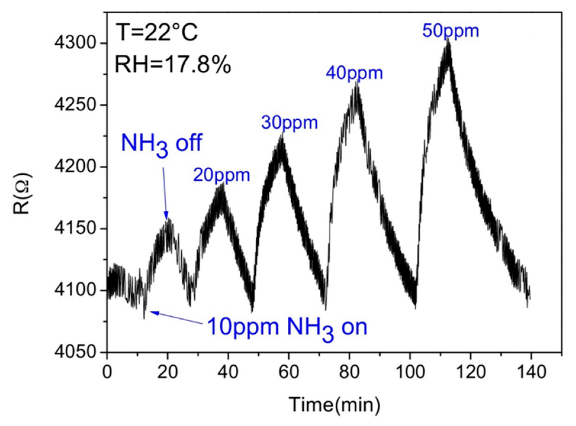
  169. Proença, M.; Rodrigues, M.S.; Vaz, F.; Borges, J. Carbon Monoxide (CO) Sensor Based on Au Nanoparticles Embedded in a CuO Matrix by HR-LSPR Spectroscopy at Room Temperature. IEEE Sens. Lett. 2021, 5, 1–3. [Google Scholar] [CrossRef]
  170. Rodrigues, M.S.; Borges, J.; Proença, M.; Pedrosa, P.; Martin, N.; Romanyuk, K.; Kholkin, A.L.; Vaz, F. Nanoplasmonic response of porous Au-TiO2 thin films prepared by oblique angle deposition. Nanotechnology 2019, 30, 225701. [Google Scholar] [CrossRef]
  171. Barranco, A.; Borras, A.; Gonzalez-Elipe, A.R.; Palmero, A. Perspectives on oblique angle deposition of thin films: From fundamentals to devices. Prog. Mater. Sci. 2016, 76, 59–153. [Google Scholar] [CrossRef] [Green Version]
  172. Abbasian, S.; Moshaii, A.; Vayghan, N.S.; Nikkhah, M. Ag Nanostructures Produced by Glancing Angle Deposition with Remarkable Refractive Index Sensitivity. Plasmonics 2017, 12, 631–640. [Google Scholar] [CrossRef]
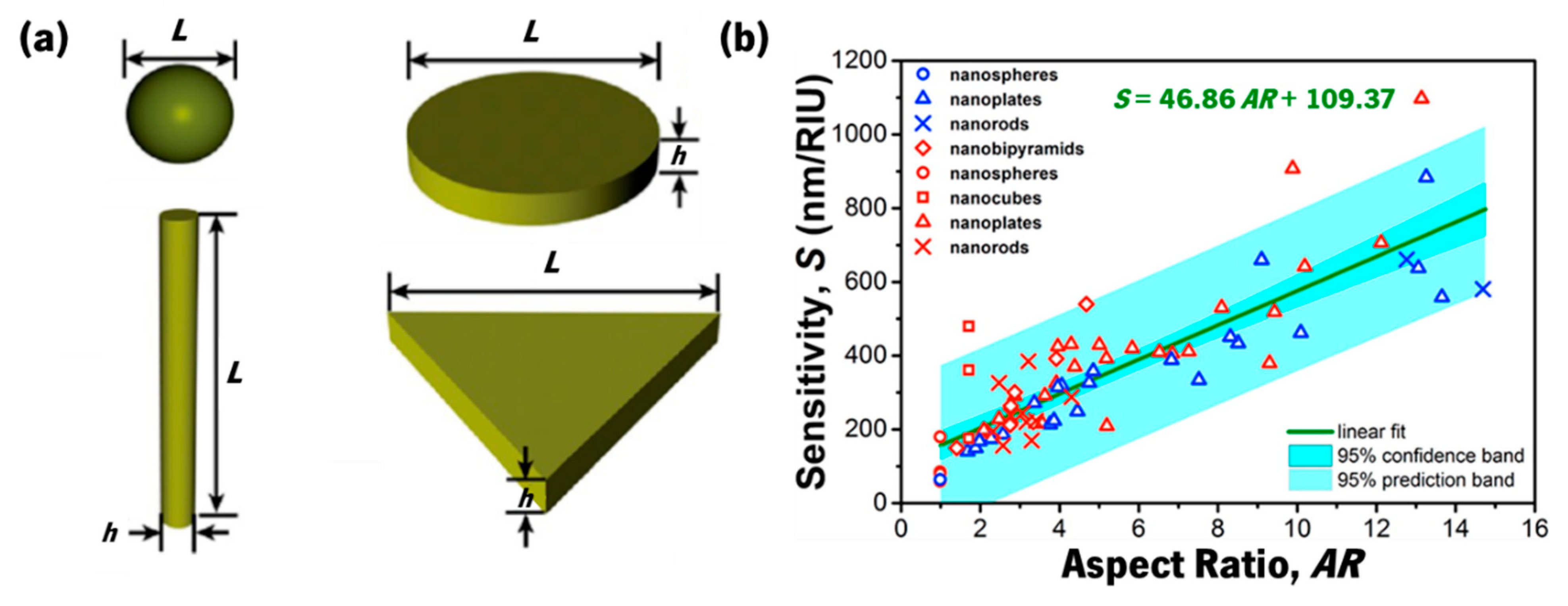
  173. Khan, A.U.; Zhao, S.; Liu, G. Key Parameter Controlling the Sensitivity of Plasmonic Metal Nanoparticles: Aspect Ratio. J. Phys. Chem. C 2016, 120, 19353–19364. [Google Scholar] [CrossRef]
  174. Edward, N.W.M.; Goswami, P. 9—Plasma-based treatments of textiles for water repellency. In The Textile Institute Book Series; Sanjay, M.R., Madhu, P., Parameswaranpillai, J., Siengchin, S., Gorbatyuk, S.M., Eds.; Woodhead Publishing: Sawston, UK, 2018; pp. 215–232. ISBN 978-0-08-101212-3. [Google Scholar]
  175. Kechkar, S. Experimental Investigation of a Low Pressure Capacitively-Coupled Discharge. Ph.D. Thesis, Dublin City University, Dublin, Ireland, 2015. [Google Scholar]
  176. Ebnesajjad, S. Chapter 9—Plasma Treatment of Polymeric Materials; William Andrew Publishing: Oxford, UK, 2014; pp. 227–269. ISBN 978-0-323-26435-8. [Google Scholar]
  177. Shishoo, R. Introduction—The potential of plasma technology in the textile industry. In Woodhead Publishing Series in Textiles; Woodhead Publishing: Oxford, UK, 2007; pp. xv–xxx. ISBN 978-1-84569-073-1. [Google Scholar]
  178. Roy Choudhury, A.K. 14—Various ecofriendly finishes. In Woodhead Publishing Series in Textiles; Woodhead Publishing: Oxford, UK, 2017; pp. 467–525. ISBN 978-0-08-100646-7. [Google Scholar]
  179. Johansson, K.S. 20—Surface Modification of Plastics. In Plastics Design Library; Second, E., Ed.; William Andrew Publishing: New York, NY, USA, 2017; pp. 443–487. ISBN 978-0-323-39040-8. [Google Scholar]
  180. Alves, M.J.; Grenho, L.; Lopes, C.; Borges, J.; Vaz, F.; Vaz, I.P.; Fernandes, M.H. Antibacterial effect and biocompatibility of a novel nanostructured ZnO-coated gutta-percha cone for improved endodontic treatment. Mater. Sci. Eng. C 2018, 92, 840–848. [Google Scholar] [CrossRef] [PubMed]
  181. Abelmann, L.; Lodder, C. Oblique evaporation and surface diffusion. Thin Solid Film. 1997, 305, 1–21. [Google Scholar] [CrossRef] [Green Version]
  182. Pedrosa, P.; Ferreira, A.; Cote, J.-M.; Martin, N.; Yazdi, M.A.P.; Billard, A.; Lanceros-Mendez, S.; Vaz, F. Influence of the sputtering pressure on the morphological features and electrical resistivity anisotropy of nanostructured titanium films. Appl. Surf. Sci. 2017, 420, 681–690. [Google Scholar] [CrossRef]
  183. Taschuk, M.T.; Hawkeye, M.M.; Brett, M.J. Glancing Angle Deposition. In Handbook of Deposition Technologies for Films and Coatings; William Andrew Publishing: Manchester, UK, 2010; ISBN 9780815520313. [Google Scholar]
  184. Martin, N.; Robbie, K.; Carpentier, L. Architecture of Thin Solid Films by the GLAD Technique. Nanomater. Surf. Eng. 2013, 1–30. [Google Scholar]
  185. Robbie, K.; Brett, M.J. Sculptured thin films and glancing angle deposition: Growth mechanics and applications. J. Vac. Sci. Technol. A 1997, 15, 1460–1465. [Google Scholar] [CrossRef]
  186. Knorr, T.G.; Hoffman, R.W. Dependence of Geometric Magnetic Anisotropy in Thin Iron Films. Phys. Rev. 1959, 113, 1039–1046. [Google Scholar] [CrossRef]
  187. Smith, D.O. Anisotropy in Permalloy Films. J. Appl. Phys. 1959, 30, S264–S265. [Google Scholar] [CrossRef]
  188. YOUNG, N.O.; KOWAL, J. Optically Active Fluorite Films. Nature 1959, 183, 104–105. [Google Scholar] [CrossRef]
  189. Hawkeye, M.M.; Brett, M.J. Glancing angle deposition: Fabrication, properties, and applications of micro- and nanostructured thin films. J. Vac. Sci. Technol. A 2007, 25. [Google Scholar] [CrossRef]
  190. Lintymer, J.; Gavoille, J.; Martin, N.; Takadoum, J. Glancing angle deposition to modify microstructure and properties of sputter deposited chromium thin films. Surf. Coat. Technol. 2003, 174–175, 316–323. [Google Scholar] [CrossRef]
  191. Besnard, A.; Martin, N.; Sthal, F.; Carpentier, L.U.C.; Rauch, J.-Y. Metal-to-Dielectric transition induced by annealing of oriented titanium thin FILMS. Funct. Mater. Lett. 2012, 6, 1250051. [Google Scholar] [CrossRef] [Green Version]
  192. Pedrosa, P.; Lopes, C.; Martin, N.; Fonseca, C.; Vaz, F. Electrical characterization of Ag:TiN thin films produced by glancing angle deposition. Mater. Lett. 2014, 115, 136–139. [Google Scholar] [CrossRef]
  193. Homola, J.; Yee, S.S.; Gauglitz, G. Surface plasmon resonance sensors: Review. Sens. Actuators B Chem. 1999, 54, 3–15. [Google Scholar] [CrossRef]
  194. Nylander, C.; Liedberg, B.; Lind, T. Gas detection by means of surface plasmon resonance. Sens. Actuators 1982, 3, 79–88. [Google Scholar] [CrossRef]
  195. Schasfoort, R.B.M.; Tudos, A.J. Handbook of Surface Plasmon Resonance; Royal Society of Chemistry: Cambridge, UK, 2008; ISBN 0854042679. [Google Scholar]
  196. Rodrigues, M.S.; Borges, J.; Gabor, C.; Munteanu, D.; Apreutesei, M.; Steyer, P.; Lopes, C.; Pedrosa, P.; Alves, E.; Barradas, N.P.; et al. Functional behaviour of TiO2 films doped with noble metals. Surf. Eng. 2015, 32, 1743294415Y.000. [Google Scholar]
  197. Borges, J.; Costa, D.; Antunes, E.; Lopes, C.; Rodrigues, M.S.; Apreutesei, M.; Alves, E.; Barradas, N.P.; Pedrosa, P.; Moura, C.; et al. Biological behaviour of thin films consisting of Au nanoparticles dispersed in a TiO2 dielectric matrix. Vacuum 2015, 122, 360–368. [Google Scholar] [CrossRef]
  198. Niu, L.; Zhang, N.; Liu, H.; Zhou, X.; Knoll, W. Integrating plasmonic diagnostics and microfluidics. Biomicrofluidics 2015, 9, 052611. [Google Scholar] [CrossRef] [PubMed] [Green Version]
  199. SadAbadi, H.; Badilescu, S.; Packirisamy, M.; Wüthrich, R. Integration of gold nanoparticles in PDMS microfluidics for lab-on-a-chip plasmonic biosensing of growth hormones. Biosens. Bioelectron. 2013, 44, 77–84. [Google Scholar] [CrossRef] [PubMed]
  200. Liu, Y.; Xie, S.; Xiao, X.; Li, S.; Gao, F.; Zhang, Z.; Du, J. Fabricating metal nanoparticle arrays at specified and localized regions of microfluidic chip for LSPR sensing. Microelectron. Eng. 2016, 151, 7–11. [Google Scholar] [CrossRef]
  201. Chen, P.; Liedberg, B. Curvature of the Localized Surface Plasmon Resonance Peak. Anal. Chem. 2014, 86, 7399–7405. [Google Scholar] [CrossRef] [PubMed]
  202. Henkel, A.; Ye, W.; Khalavka, Y.; Neiser, A.; Lambertz, C.; Schmachtel, S.; Ahijado-Guzmán, R.; Sönnichsen, C. Narrowing the Plasmonic Sensitivity Distribution by Considering the Individual Size of Gold Nanorods. J. Phys. Chem. C 2018, 122, 10133–10137. [Google Scholar] [CrossRef]
  203. Søndergaard, T. Modeling of plasmonic nanostructures: Green’s function integral equation methods. Phys. Status Solidi 2007, 244, 3448–3462. [Google Scholar] [CrossRef]
  204. Khlebtsov, N.G. T-matrix method in plasmonics: An overview. J. Quant. Spectrosc. Radiat. Transf. 2013, 123, 184–217. [Google Scholar] [CrossRef]
  205. Siad, A.; Besnard, A.; Nouveau, C.; Jacquet, P. Critical angles in DC magnetron glad thin films. Vacuum 2016, 131, 305–311. [Google Scholar] [CrossRef] [Green Version]
  206. Sun, F.; Du, C.; Fu, T.; Chen, Y.; Sun, L.; Zhang, R.; Shi, D. Optimal aspect ratio and excitation spectral region of individual AuxAg1−x alloy nanobars for plasmonic sensing. Phys. Lett. A 2020, 384, 126785. [Google Scholar] [CrossRef]
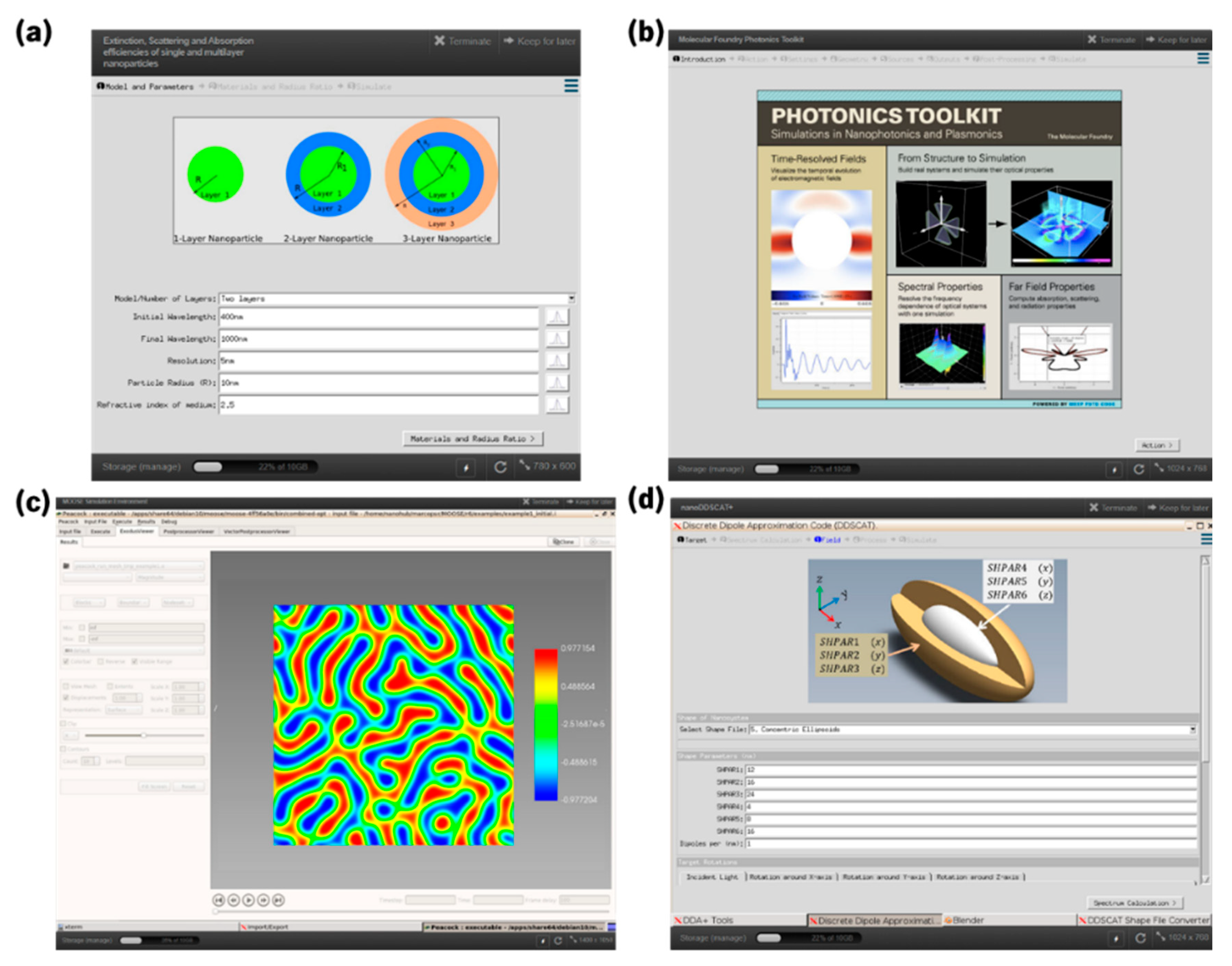
  207. Madhavan, K.; Zentner, L.; Farnsworth, V.; Shivarajapura, S.; Zentner, M.; Denny, N.; Klimeck, G. nanoHUB.org: Cloud-based services for nanoscale modeling, simulation, and education. Nanotechnol. Rev. 2013, 2, 107–117. [Google Scholar] [CrossRef]
  208. Camden, J.; Schatz, G.C. Nanosphere Optics Lab. 2016. Available online: https://nanohub.org/resources/nsoptics (accessed on 1 May 2021).
  209. Krishna, J.B.; Jun, H.; Lasse, J. Extinction, Scattering and Absorption Efficiencies of Single and Multilayer Nanoparticles; Pennsylvania State University: Centre County, PA, USA, 2016. [Google Scholar]
  210. McLeod, A.S.; Schuck, P.J.; Neaton, J.B. Molecular Foundry Photonics Toolkit; University of California: Berkeley, CA, USA, 2020. [Google Scholar]
  211. Permann, C.J.; Gaston, D.R.; Andrš, D.; Carlsen, R.W.; Kong, F.; Lindsay, A.D.; Miller, J.M.; Peterson, J.W.; Slaughter, A.E.; Stogner, R.H.; et al. MOOSE: Enabling massively parallel multiphysics simulation. SoftwareX 2020, 11, 100430. [Google Scholar] [CrossRef]
  212. Clark, S.; Aagesen, L.; Schwen, D. MOOSE (Multi-physics Object Oriented Simulation Environment). 2020. Available online: https://nanohub.org/resources/moose (accessed on 1 May 2021).
  213. Sobh, A.N.; White, S.; Smith, J.; Sobh, N.; Jain, P.K. nanoDDSCAT+. 2019. Available online: https://nanohub.org/resources/ddaplus (accessed on 1 May 2021).
  214. Parsons, J.; Burrows, C.P.; Sambles, J.R.; Barnes, W.L. A comparison of techniques used to simulate the scattering of electromagnetic radiation by metallic nanostructures. J. Mod. Opt. 2010, 57, 356–365. [Google Scholar] [CrossRef]
  215. Loke, V.L.Y.; Huda, G.M.; Donev, E.U.; Schmidt, V.; Hastings, J.T.; Mengüç, M.P.; Wriedt, T. Comparison between discrete dipole approximation and other modelling methods for the plasmonic response of gold nanospheres. Appl. Phys. B 2014, 115, 237–246. [Google Scholar] [CrossRef]
  216. Mencarelli, E.; Fanò, L.; Tarpani, L.; Latterini, L. Modelling the Optical Properties of Metal Nanoparticles: Analytical vs Finite Elements Simulation. Mater. Today Proc. 2015, 2, 161–170. [Google Scholar] [CrossRef]
  217. Dhawan, A.; Norton, S.J.; Gerhold, M.D.; Vo-Dinh, T. Comparison of FDTD numerical computations and analytical multipole expansion method for plasmonics-active nanosphere dimers. Opt. Express 2009, 17, 9688–9703. [Google Scholar] [CrossRef]
  218. Bora, T.; Dousse, A.; Sharma, K.; Sarma, K.; Baev, A.; Hornyak, G.L.; Dasgupta, G. Modeling nanomaterial physical properties: Theory and simulation. Int. J. Smart Nano Mater. 2019, 10, 116–143. [Google Scholar] [CrossRef] [Green Version]
  219. Liebsch, A.; González, P.V. Optical properties of randomly distributed particles. Phys. Rev. B 1984, 29, 6907–6920. [Google Scholar] [CrossRef]
  220. MacMillan, M.F.; Devaty, R.P.; Mantese, J.V. Infrared properties of Pt/Al2O3 cermet films. Phys. Rev. B 1991, 43, 13838–13845. [Google Scholar] [CrossRef]
  221. Vasilevskiy, M.I.; Anda, E.V. Effective dielectric response of semiconductor composites. Phys. Rev. B 1996, 54, 5844–5851. [Google Scholar] [CrossRef] [Green Version]
  222. Diaz-HR, R.; Esquivel-Sirvent, R.; Noguez, C. Plasmonic Response of Nested Nanoparticles with Arbitrary Geometry. J. Phys. Chem. C 2016, 120, 2349–2354. [Google Scholar] [CrossRef]
  223. Shalaev, V.M. Nonlinear Optics of Random Media; Springer Tracts in Modern Physics; Springer: Berlin/Heidelberg, Germany, 2000; Volume 158, ISBN 978-3-540-65615-9. [Google Scholar]
  224. DeVoe, H. Optical Properties of Molecular Aggregates. I. Classical Model of Electronic Absorption and Refraction. J. Chem. Phys. 1964, 41, 393–400. [Google Scholar] [CrossRef]
  225. Purcell, E.M.; Pennypacker, C.R. Scattering and Absorption of Light by Nonspherical Dielectric Grains. Astrophys. J. 1973, 186, 705. [Google Scholar] [CrossRef]
  226. Draine, B.T.; Flatau, P.J. Discrete-Dipole Approximation for Scattering Calculations. J. Opt. Soc. Am. A 1994, 11, 1491–1499. [Google Scholar] [CrossRef]
  227. Draine, B.T. The discrete-dipole approximation and its application to interstellar graphite grains. Astrophys. J. 1988, 333, 848. [Google Scholar] [CrossRef]
  228. Goodman, J.J.; Draine, B.T.; Flatau, P.J. Application of fast-Fourier-transform techniques to the discrete-dipole approximation. Opt. Lett. 1991, 16, 1198–1200. [Google Scholar] [CrossRef]
  229. Jain, P.K.; Lee, K.S.; El-Sayed, I.H.; El-Sayed, M.A. Calculated Absorption and Scattering Properties of Gold Nanoparticles of Different Size, Shape, and Composition:  Applications in Biological Imaging and Biomedicine. J. Phys. Chem. B 2006, 110, 7238–7248. [Google Scholar] [CrossRef] [PubMed] [Green Version]
  230. Johnson, P.B.; Christy, R.W. Optical Constants of the Noble Metals. Phys. Rev. B 1972, 6, 4370–4379. [Google Scholar] [CrossRef]
  231. van Dijk, M.A.; Tchebotareva, A.L.; Orrit, M.; Lippitz, M.; Berciaud, S.; Lasne, D.; Cognet, L.; Lounis, B. Absorption and scattering microscopy of single metal nanoparticles. Phys. Chem. Chem. Phys. 2006, 8, 3486–3495. [Google Scholar] [CrossRef] [PubMed] [Green Version]
  232. Ruan, Q.; Fang, C.; Jiang, R.; Jia, H.; Lai, Y.; Wang, J.; Lin, H.-Q. Highly enhanced transverse plasmon resonance and tunable double Fano resonances in gold@titania nanorods. Nanoscale 2016, 8, 6514–6526. [Google Scholar] [CrossRef] [PubMed]
  233. Gisbert Quilis, N.; Lequeux, M.; Venugopalan, P.; Khan, I.; Knoll, W.; Boujday, S.; Lamy de la Chapelle, M.; Dostalek, J. Tunable laser interference lithography preparation of plasmonic nanoparticle arrays tailored for SERS. Nanoscale 2018, 10, 10268–10276. [Google Scholar] [CrossRef] [PubMed] [Green Version]
  234. Proença, M.; Rodrigues, M.S.; Borges, J.; Vaz, F. Optimization of Au:CuO Nanocomposite Thin Films for Gas Sensing with High-Resolution Localized Surface Plasmon Resonance Spectroscopy. Anal. Chem. 2020, 92, 4349–4356. [Google Scholar] [CrossRef]
  235. Hawkeye, M.M.; Taschuk, M.T.; Brett, M.J. Glancing Angle Deposition of Thin Films; John Wiley & Sons, Ltd.: Chichester, UK, 2014; ISBN 9781118847510. [Google Scholar]
Figure 1. Simplified schematics of the human olfactory system (adapted from Lafreniere and Mann [2], copyright 2009 Elsevier).
Applsci 11 05388 g001
Figure 2. (a-i) Schematics of the experimental circuit used by Brattain and Bardeen in 1953 that used germanium and a platinum reference electrode to demonstrate a resistance-dependence on the surrounding atmosphere, and (a-ii) contact potential measured in a monitoring cycle when germanium is exposed to wet O2 and dry O2 (reused with permission of Nokia Corporation and AT&T Archives, from Brattain and Bardeen [3]). (b) Effect of electrode metal on response amplitude at polarization current of 6 × 10⁻⁷ A (adapted with permission from Wilkens and Hartman [5], copyright 2006 John Wiley and Sons).
Applsci 11 05388 g002
Figure 3. Response of a reduced graphene oxide-based gas sensor (adapted from Li et al. [8], copyright 2016 Elsevier).
Applsci 11 05388 g003
Figure 4. (a) Lycurgus Cup, a Roman glass from the fourth century AD, depicting a mythological scene, with King Lycurgus being entangled by Ambrosia, which was transformed into a vine-shoot by Dionysus (the Greek god of wine), currently held at the British Museum, London; it looks (a-i) “opaque pea-green” with reflected light, and (a-ii) “deep wine-red” with transmitted light (copyright 2021 The Trustees of the British Museum), due to (a-iii) Ag-Au alloy nanoparticles (adapted from Barber and Freestone [32], copyright 2007 John Wiley and Sons). (b) Glass cups coated at CF-UM-UP, University of Minho, with different nanocomposite thin films (1–uncoated glass; 2–Au-TiO2 with low gold concentration; 3–Au-TiO2 with higher gold concentration; and 4–Au-Al2O3) showing different colours with (b-i) reflected light and (b-ii) transmitted light.
Applsci 11 05388 g004
Figure 5. (a) Notre-Dame Cathedral, Paris showing the south facade, and the southern rose window, photographed from (b-i) inside and (c-i) outside. A detail of the southern rose window photographed from (b-ii) inside and (c-ii) outside (mirrored) (adapted with permission from Pascal Lemaitre Photographe, copyright 2021).
Applsci 11 05388 g005
Figure 6. (a) Schematics of localized surface plasmons of a metal sphere. (b) Schematics of a typical LSPR band, measured in transmittance mode, and extinction spectrum.
Applsci 11 05388 g006
Figure 7. Influence of Au nanoparticles size, shape, and surrounding dielectrics on the LSPR band curvature and colour. (a) SEM images of colloidal Au nanoparticles with increasing size, corresponding colours, and LSPR band by UV–Vis spectroscopy (adapted from Notarianni et al. [61], copyright 2014 Elsevier); (b) TEM images of 30 nm Au nanoparticles, and photographs of the same Au nanoparticles immersed in water and poly(vinyl alcohol) (PVA) (adapted from Pluchery et al. [62]. copyright 2013 Springer); (c) TEM images of Au nanospheres, nanorods, and nanostars, with the corresponding LSPR observed by UV–Vis spectroscopy and colour (adapted from Adnan et al. [58], copyright 2016 The Royal Society of Chemistry). (d) Colloidal gold nanorods solutions with six different colours and their corresponding UV–Vis extinction spectra, and TEM images showing the nanorods with different aspect ratios (AR) (adapted with permission from Zhang et al. [59], copyright 2016 The Optical Society).
Applsci 11 05388 g007
Figure 8. (a) Illustration of strategies used to develop plasmonic nanosensors (adapted from Guo et al. [64], copyright 2015 Elsevier). (b) Schemes for LSPR biosensors through extinction measurement, total internal reflection measurement, and darkfield measurement microscopy (adapted from Lopez et al. [70], copyright 2016 De Gruyter). (c) Schematic of an ordered gold nanorod array chip for plasmon-enhanced fluorescence (PEF) DNA detection based on a molecular beacon (adapted from Mei and Tang [72], copyright 2017 American Chemical Society). (d) Schematic of a localized surface plasmon amplification by stimulated emission of radiation (spaser) as a multimodal cellular nanoprobe (adapted from Ekaterina et al. [83], copyright 2017 Springer Nature). (e) PET/CT coregistered images of mice intravenously administrated with either saline or Au nanocages, followed by laser treatment. A—saline-injected mouse prior to laser irradiation; B—nanocage-injected mouse prior to laser irradiation; C—saline-injected mouse after laser irradiation; and D—nanocage-injected mouse after laser irradiation. (adapted from Chen et al. [86], copyright 2010 John Wiley and Sons).
Applsci 11 05388 g008
Figure 9. (a) Illustration of a TiO2 thin film sensor along with AFM topography of the TiO2 thin film surface. Plots showing, at the top, the sensor resistance, as a function of the top electrode width, for 0 and 10,000 ppm of H2 at room temperature, 50, and 100 °C and, at the bottom, the corresponding response of the sensors at room temperature (adapted from Plecenik et al. [109], copyright 2015 Elsevier). (b) Optical microscopy image of a microheater coated in the centre with a sensing p-type CuO semiconducting layer. Comparison of the response obtained under dynamic tests in the full temperature range (20–500 °C, 0 to 55 mW heating) (adapted from Presmanes et al. [110], copyright 2017 MDPI).
Applsci 11 05388 g009
Figure 10. Examples of vacuum chemical vapour deposition (CVD) methods (a,b) and physical vapour deposition (PVD) methods (ce). Simplified schematic figure of (a) metal–organic chemical vapour deposition (MO–CVD), (b) plasma enhanced chemical vapour deposition (PE-CVD), (c) reactive magnetron sputtering, (d) resistance heating, and (e) electron beam evaporation.
Applsci 11 05388 g010
Figure 11. Schematic figures of (a) basic sputtering configuration; (b) the target surface, showing the important species and processes that take place during sputtering; (c) magnetron sputtering configuration; and (d) target and the preferential erosion zone as a result of the magnetic field of the magnetron that causes a local electron confinement (adapted from Bräuer et al. [148], copyright 2010 Elsevier).
Applsci 11 05388 g011
Figure 12. Schematics of a custom-made reactive DC magnetron sputtering vacuum chamber showing the placement of noble metal “pellets” (adapted from Domingues et al. [153], copyright 2019 Elsevier).
Applsci 11 05388 g012
Figure 13. Sequence of SEM micrographs of nanocomposite Au–TiO2 thin films during an in situ thermal treatment experiment, from room temperature (thin film after deposition by reactive magnetron sputtering) up to 400 °C. The labels I, II, and III show different nanoparticles at different moments that appeared due to the migration of dissolved Au atoms. Micrographs were taken and processed by Marco S. Rodrigues et. al. using a FEI QUANTA 650 FEG scanning electron microscope.
Applsci 11 05388 g013
Figure 14. (a) Low-pressure plasma treatment simplified schematics. (b) Simplified schematics of a commercial cylindrical low-pressure capacitively coupled plasma system with optimized electrode shape for uniform surface.
Applsci 11 05388 g014
Figure 15. Simplified schematics of (a) sputtering and GLAD sample holder position and α/φ motion, relative to the sputtering target, for the production of, e.g., zigzag thin films, and (b) growth of inclined columns on a substrate when the sputtered particles arrive at an angle α from the normal to the substrate. A growth competition occurs between columns due to the shadowing effect created by the columns themselves (self-shadowing), thus creating spaced columns tilted at an angle β. (c) Example of a GLAD deposition process for the production of one zigzag cycle.
Applsci 11 05388 g015
Figure 16. SEM micrographs of GLAD-sculptured TiO2 thin films. Cross-sectional SEM images of (a) zigzag nanocolumns, (b) spiral nanocolumns, (c) zigzag plus spiral nanocolumns, (d) nanocolumns with width modulation, and (e) vertical columns (adapted from Barranco et al. [171], copyright 2016 Elsevier).
Applsci 11 05388 g016
Figure 17. Refractive index sensing using LSPR in gold nanoparticles with a water drop on top. A clear (a) colour change and (b) LSPR band shift can be seen between the areas covered by air ( n s 1.00) and water ( n s 1.33.
Applsci 11 05388 g017
Figure 18. (a) Shapes of nanoparticles synthesized and investigated by Khan et al. [173], including nanodisks, nanoprisms, nanorods, and nanospheres, with different aspect ratio (AR = L/h). (b) Measured sensitivities (S, or RIS) of nanoparticles of various sizes, shapes, and compositions. The sensitivity follows a linear relationship with the aspect ratio, regardless of nanoparticle shape, size, and composition (adapted from Khan et al. [173], copyright 2016 American Chemical Society).
Applsci 11 05388 g018
Figure 19. Simulation tools available at Nanohub using the computational power of super computers: (a) Extinction, Scattering and Absorption Efficiencies of Single and Multilayer Nanoparticles [209]; (b) Molecular Foundry Photonics Toolkit [210], (c) MOOSE [211,212]; and (d) nanoDDSCAT+ [213].
Applsci 11 05388 g019
Figure 20. Optical extinction efficiency coefficient of spheroidal Au nanoparticles with similar volumes and different aspect ratio (a) AR = 1, (b) AR = 2, (c) AR = 3, and (d) AR = 4, and different surrounding refractive indices ( n s = 1.0, 1.3, and 1.5). (e) Plot of wavelenght shift ( Δ λ ) against Δ n s using data taken from (ad), and linear fit for each nanoparticle shape to estimate the RIS using the slope. Simulated using nanoDDSCAT+ tool [213].
Applsci 11 05388 g020
Figure 21. Au nanoparticles with similar volumes, without or with a layer of 4 or 8 nm TiO2, with different surrounding refractive indices ( n s = 1.0, 1.3, and 1.5) and different shapes: (a) sphere, AR = 1, (b) oblate spheroid with AR = 2, and (c) prolate spheroid with AR = 2. Optical extinction efficiency coefficient of the (d) Au spheres, (e) oblate spheroid, and (f) prolate spheroid. Plots of Δ λ against Δ n s (gi) using data taken from (df), respectively, to estimate the sensitivity (RIS). Simulated using nanoDDSCAT+ tool, available at nanoHuB.org [213].
Applsci 11 05388 g021
Table 1. Odour molecules’ ordered pathway comparison in the olfactory and electronic nose systems.
Olfactory SystemElectronic Nose System
i. Nostril i. Sampler
ii. Primary neuronsii. Sensor array
iii. Secondary neuronsiii. Signal conditioning and processing
iv. Brainiv. Pattern recognition
Table 2. World market projection for sensors, 2024.
Sensor TypeProjected Market (M EUR)
Chemical sensors—Worldwide36,100 [25]
Gas sensors—Worldwide1400 [26]
Gas sensors—Europe360 [26]
Table 3. Estimated RIS results for all the Au nanoparticle shapes and the TiO2 overlayer thicknesses.
Au Nanoparticle Aspect Ratio and ShapeTiO2 Layer Thickness on Au Nanoparticle (nm)RIS (nm.RIU−1)
1 (sphere)-52
1 (sphere)433
1 (sphere)821
2 (prolate)-158
2 (prolate)474
2 (prolate)846
2 (oblate) 106
2 (oblate)457
2 (oblate)839
3 (prolate)-305
4 (prolate)-414
Publisher’s Note: MDPI stays neutral with regard to jurisdictional claims in published maps and institutional affiliations.

