
Warpage Behavior on Silicon Semiconductor Device: The Impact of Thick Copper Metallization


1
Automotive and Discrete Group, R&D Department, STMicroelectronics, 95121 Catania, Italy
2
Dipartimento di Ingegneria Elettrica, Elettronica ed Informatica (DIEEI), Università degli Studi di Catania, 95125 Catania, Italy
*
Author to whom correspondence should be addressed.
Appl. Sci. 2021, 11(11), 5140; https://doi.org/10.3390/app11115140
Submission received: 13 May 2021
/
Revised: 26 May 2021
/
Accepted: 28 May 2021
/
Published: 1 June 2021
(This article belongs to the Special Issue New Trends in Design Engineering)
Abstract
:Electrochemical deposited (ECD) thick film copper on silicon substrate is one of the most challenging technological brick for semiconductor industry representing a relevant improvement from the state of art because of its excellent electrical and thermal conductivity compared with traditional materials, such as aluminum. The main technological factor that makes challenging the industrial implementation of thick copper layer is the severe wafer warpage induced by Cu annealing process, which negatively impacts the wafer manufacturability. The aim of presented work is the understanding of warpage variation during annealing process of ECD thick (20 μm) copper layer. Warpage is experimentally characterized at different temperature by means of Phase-Shift Moiré principle, according to different annealing profiles. Physical analysis is employed to correlated the macroscopic warpage behavior with microstructure modification. A linear Finite Element Model (FEM) is developed to predict the geometrically stress-curvature relation, comparing results with analytical models.
1. Introduction
Formation of copper thick film on silicon substrate is desirable in the semiconductor industry because of its excellent electrical and thermal conductivity [1,2]. Compared to other materials, such as aluminum, these properties allow us, respectively, to reduce the Joule effect and help the efficient dissipation of heat generated during operation. Furthermore, Cu metallization is better than aluminum in terms of resistance to electromigration and stress voiding phenomena [3,4]. The main technique to produce thick copper film on silicon substrate is electrochemical deposition (ECD), which is a highly efficient wet process for depositing a uniform layer of metal (like copper) on a semiconductor wafer [5,6]. Furthermore, Cu front metal is very attractive for integrated circuit (IC) manufacturing because it enables high-reliable Cu-Cu wire bonding solution [7,8,9,10]. The integration of Cu into ICs is still a technical challenge due to the induced stress in back end of line structures [11,12] and due to the severe wafer warpage induced by Cu annealing, which affects the accuracy of the subsequent manufacturing processes, such as the wafer handle and the adsorption of vacuum suction cup, having also a negative impact on device reliability. Wafer warpage caused by thick Cu layer is mostly due to plastic deformation during the annealing [13], which is a thermal process aimed to make softer Cu material, increasing and then stabilizing the Cu grains dimension. Stabilizing metal grain size, annealing permits to avoid electromigration issues in interconnect reliability, e.g., during reliability application related test [14,15,16,17] or passive thermal cycles [18,19]. It seems to miss in literature a detailed experimental warpage analysis for thick Cu layer: available data refer about maximum 5 μm thick Cu metal [3,20]. As later discussed, some analytical models are developed to calculate stress and warpage due to thermal budget. However, current approaches cannot account material no-linearity and they assume only simple geometries, such as wafer or rectangular beam. A dedicated numeric model should be useful to overcome the above mentioned limitations.
The scope of this work is to characterize experimentally the warpage, which is intended as the maximum deflection, induced by 20 μm thick Cu film on a rectangular wafer slice, considering two different annealing profiles. The considered sample and tests are described in Section 2 and the working principle of warpage measurements are reported in Section 3.1. Results in terms of warpage are presented in Section 3.2 and dedicated physical analysis is employed and presented in Section 3.3 to clarify the phenomenology behind the observed warpage. Two numerical approaches [21,22] to calculate warpage due to a thermal input are resumed in Section 4.1. A Finite Element Model (FEM) is developed to predict the stress-curvature relation inside the elastic regime. Numerical outcomes are compared with the results of Stoney and Timoshenko equations as reported in Section 4.2. The final target of this paper is to correlate the warpage behavior of silicon devices with thick (20 μm) ECD copper film with physical modification induced by thermal treatment, such as annealing, and to find out a reliable numerical model to predict warpage. An analysis on micro-structure evolution due temperature evolution in the range between 150 and 250 permits to understand if it is possible optimize manufacturing process to reduce the residual warpage.
2. Sample and Test Description
The considered samples for warpage analysis are 50 × 10 × 0.75 mm beam, made by bulk Silicon 730 μm-thick, TiW 0.3 μm, Cu seed 0.2 μm, and ECD Copper 20 μm-thick. These portions are sliced from wafer just after copper electro-deposition at room temperature; therefore, copper is not thermally treated before samples formation. The slices are annealed following three different temperature profile, shown in Figure 1. Considering that the experiments analyze the impact of annealing process on wafer warpage, it is assumed that the trends discovered by these measurements on rectangular slices are valid also for wafer. As first approach, according to Timoshenko’s theory later reported in Section 4.1, the ratio between 8-inches (200 mm) wafer and rectangular slice (50 mm) deflection could be calculated from Equation (7), resulting equal to 8.
The ramps are characterized by fixed heating and cooling rate (respectively, 10 and 5 C/min) and setting the maximum temperature at 250 (in profiles “W/ plateau” and “W/o plateau”) or 150 C (in profile “150 C”). The profile “W/ plateau” has a period of 30 min (the so called “plateau”) in which temperature dwells at 250 C. The two temperature values are quite lower than the real process annealing temperature and they are chosen to analyze the warpage behavior due to copper film modification induced by Cu grain growth. As later shown by DSC analysis, an exothermic reaction happens at around 160 . The profile “W/o plateau” is repeated three times to investigate on hysteretic behavior after the first cycle. Warpage is measured continuously during the annealing, according to methodology explained in the following paragraph. Due to simple geometrical considerations, beam curvature is derived from warpage and compared with the calculated by Finite Element Model in linear elastic regime. Physical analysis is performed to clarify the physical modifications that occurs in copper during thermal profile. With respect to the samples considered for warpage measurements, it is used for physical analysis samples with AlCu metal and TEOS passivations layers placed between the TiW layer of and the silicon substrate. The difference between warpage and physical analysis sample is negligible for the sake of the present work because the scope of physical analysis is to highlight thick copper micro-structure modification due to different temperature input. These interleaved layers between thick copper and silicon substrate do not affect copper structure modification due to thermal budget.
3. Warpage Measurements and Physical Analysis
3.1. Method Description for Warpage Measurements
A method based on Moirè Phase Shift is considered to experimentally quantify the warpage, using the commercial equipment “TDM (Topography and Deformation Measurements) Compact” by Insidix [23] presented in Figure 2.
Analyzed sample is illuminated by a stripe pattern, which interacts with sample’s surface structure. This image is captured by a Charge-Coupled Device (CCD) camera, that correlates the resulting pattern modification with surface out-of-plane deformation of each sample point. The equipment is made by two main parts: the projection (composite light source) and the viewing (CCD camera + optics) systems. The first is a common projector, which projects strip patterns piloted by software. The viewing system includes a CCD camera and the viewing lens. When using phase-shift projection Moiré, the camera grating is phase-shifted against the projection grating. This technique can be applied for accurate 3D reconstruction. The equipment can regulate chamber temperature by infrared lamps and air cooler by a proportional–integral–derivative (PID) controller, in which the feedback is given by the temperature measured in real time by a thermocouple directly attached to measurement stage. The schematic of experimental equipment is reported in Figure 3.
In the digital projection Moiré option, the considered methodology for the presented analysis, the camera grating is imaged directly by software. The acquired image is numerically demodulated in order to make the sample profile reconstruction. The transmission of the square wave gratings through the optical system can be approximated as a cosine function of the profile number. Thus, the intensity pattern projected onto the object surface through the projection lens () is described as:
where is the intensity of the light source, is the reflectance, and A and are, respectively, amplitude and profile number of the projection grating. Meanwhile, the virtual intensity pattern on the sample (), coming from viewing system, could be described by:
where is the profile number of the viewing grating line that virtually illuminates the point (x, y). This described overlap generates an interference pattern, which can be expressed [24]:
in which is the recorded fringe interference pattern for the k-th shift (), d is the distance between the light source and the observer, h is the distance from the grating to the light source and observer, z is the out-of-plane deformation of measured surface, p is the pitch of the Moirè grating, and and are, respectively, the background and local contrast. In order to find out z, deleting experimental noise, measurements are performed with different m grating pitches, as explicated in Equation (3) by terms . Considering a Gaussian least squares approach, it is possible to solve iteratively the m equations (one for each considered phase-shift), non-linear in the coordinate z. The described approach is practically implemented by the used equipment considering a “virtual” grating, according to Reference [24].
3.2. Results
The measurement outputs considered for the presented work are the warpage maps shown in Figure 4, captured at different time of temperature profile, during both the heating and cooling phases.
In particular, Figure 4 shows the acquisition for the first cycle of “W/o plateau” sample; meanwhile, similar analyses are performed for other test vehicles. Starting from the warpage maps, they are extracted warpage profiles along a specific vertical cutline, as depicted in Figure 6.
Warpage-temperature behavior is plotted in Figure 5, following the sign convention declared in Figure 4 and reporting the maximum warpage resulting in cutline extrapolation for each map, explained in Figure 6. It is arbitrarily chosen to consider the warpage positive in case of crying (convex) shape and a negative value in case of smiling (concave) shape. Analysis highlights that annealing process modifies warpage at 50 C in all temperature profiles. Warpage is at the start, whereas it becomes around at the end of first cycle considering profiles “W/Plateau” and “W/o Plateau”, while it becomes around for “150 C” profile. A possible explanation could be grain size growth is “freeze” and not completed in “150 C” profile with respect to other temperature profiles with maximum temperature of 250 C. Looking to the second cycle, warpage behaves as a closed loop because there is no warpage modification between the start and the end of cycle at 50 C. Warpage is modified during 30 min plateau at 250 from around at the start of plateau to at the end of plateau. However, no significant difference is carried out after the cooling at room temperature. It is observed the first part of warpage-temperature diagram in the second cycle (between 50 and 90 C) has a linear trend. The incremental ratio between warpage variation and temperature in this range is considered to benchmark the different warpage calculation methods presented in following paragraph. The warpage trend in temperature during the heating phase shows a change in slope that occurs at 150 C, at which warpage reaches its maximum. This observed behavior could indicate an irreversible phenomenon in copper layer: the dedicated physical analysis will help to better understand the phenomenology as reported in Section 3.3.
3.3. Physical Analysis
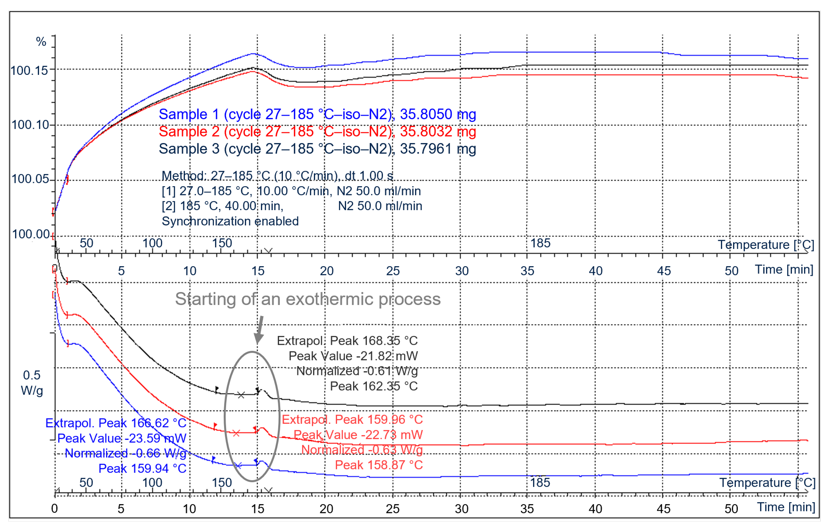
Differential Scanning Calorimetry (DSC) analysis is employed to detect the occurrence of thermally driven phenomenon during the heating process. A sample identical to the ones considered for warpage measurements is heated from room temperature to 185 with an heating rate of 10 /min. DSC analysis reported in Figure 7 highlights the starting of an exothermic reaction at 160 . It could be indicative of an irreversible modification of the copper layer that it will be further investigated by microscopy.
Some samples are cross-sectioned and analyzed by Focused Ion Beam (FIB) technique [25]. Devices under test are milled with high precision by FIB and without splashing the copper metal and creating artefact due to sample preparation. The FIB-prepared samples are analyzed with Scanning Electron Microscopy (SEM). It works in a similar way as FIB, adopting a electron beam to hit the target. Information about the surface topography and composition can be extracted by the interaction between beam electrons and the the atoms on the surface sample. Comparative pictures are shown in Figure 8 for samples without thermal treatment (a), heated at 150 (b) and at 250 . Microscopy analysis points out the increase of grain size between samples treated at 150 and at 250 . Grains of thick copper layer can be distinguished among them by the different gray tonality in SEM analysis. Investigation is focused on the FIB-opened section of ECD copper film; in fact, the original not-removed thick copper film is visible on the right and left edges of Figure 8b,c. According to sample description reported at the end of Section 2, SEM points out, respectively, the metal (gray) and the TEOS (black) layers underneath ECD copper. The observed micro-structure modification is coherent with DSC result (Figure 7) that detects an irreversible thermal process at around 160 . Moreover, this observation helps to explain the warpage behavior (Figure 5), in terms of residual warpage after thermal process and slope modification in warpage/temperature curve observed at around 150 . The experimentally observed grain growth due to temperature increase is supported by literature Chaudhari model for grain growth [26].
4. Model for Warpage Calculation
4.1. Literature Analytical Approaches
Two analytical approaches aimed to predict stress and warpage are described in this section. Stoney’s equation [22,27,28] are commonly used as reference. This formula is developed for “membrane-like” geometries made by two materials, such as the system made by semiconductor wafer and ECD metal, in which one layer (in our case, ECD Cu) is much thinner than other. According to Stoney, thermal stress of thin film can be written as:
in which the Young’s modulus, the Poisson’s ratio and the thickness of the substrate, is the thickness of the film, and R and the curvature radii of the substrate after and before film deposition. Considering that thermal stress is given by , in which and are the coefficient of thermal expansion, respectively, for substrate and film. Curvature could be calculated from Stoney as follows:
The application of Stoney approach requires materials must be homogeneous and with linear elastic behavior. Considering the complex non-linear Cu behavior during annealing, Stoney results are not reliable to predict stress and warpage during the entire annealing process.
The second considered approach to numerically estimate stress comes from Timoshenko formulation for bi-material thermistors [21] that is extended for three and more materials [29,30]. This theory permits to translate the thermal input into a set of equivalent forces and momentum; therefore, it is possible to apply the classic theory for an elastic beam. Consider a beam consisting of two layers of different metals, welded together and subjected to a quasi-static temperature change from to T. If the linear thermal expansion coefficients of these two materials are different from each other, heating and cooling will generate the lamina bending. Let be and the linear thermal expansion coefficients of substrate ans film, respectively. Furthermore and represent the elasticity modules and the thickness of the two materials. For simplicity, the beam has a unit width. Considering that and are, respectively, the inertia momentum for film and substrate, curvature can be expressed as in Equation (6):
Considering a beam of length l, much smaller than the radius of curvature, the maximum deflection delta can be well approximated as:
The stress state within each lamina will be the composition of the stress induced by the bending moment M, obviously dependent on the distance from the neutral axis of the under beam, and from the axial load P, constant on each of the two parts. Bending moment can be obtained according to , in which I is the moment of geometric inertia of the cross section and R the radius of curvature of the inflexed beam. Normal load can be expressed from the equation related to flexural moment equilibrium:
Considering the cooling case, the normal load expressed in Equation (8) acts as compressive stress in the material with the lower coefficient of thermal expansion (silicon substrate), as tensile stress where the CTE is higher (thick copper film). Remembering that the beam has a unitary thickness, the total stress will be:
in which y is the distance from the neutral axis, which is placed in the median section of the beam. As well as Stoney’s formula, Timoshenko’s approach is limited by elastic material hypothesis.
4.2. Finite Element Model for Warpage Calculation
A Finite Element Model is developed with Comsol Multiphysics to calculate the warpage variation, curvature and mechanical stress due to temperature variation, inside the range between 50–90 C, in which warpage variation is found linear. It is created a 3D model, considering a simplified stack. Modeled structure is a 50 × 10 × 0.75 mm beam, made by silicon substrate (thickness 730 μm) and ECD copper layer (thickness 20 μm), neglecting TiW (0.3 μm) and seed Cu (0.2 μm) layers. These are neglected due to their lower thickness. Geometry is discretized with linear hexa mesh, not-coherent between silicon and copper due to the huge thickness difference. Considering that aim of analysis is to estimate stress and deformation inside a well-defined temperature range, materials are imposed “stress and strain free” at 50 C and then they are heated up to 90 C. Cu and Si are joined together using a “continuity” contact formulation, which fixes to 0 the relative displacements between Si and Cu nodes in contact. Displacement boundary conditions are imposed on structure vertices in order to allow the beam free expansion along the three directions.
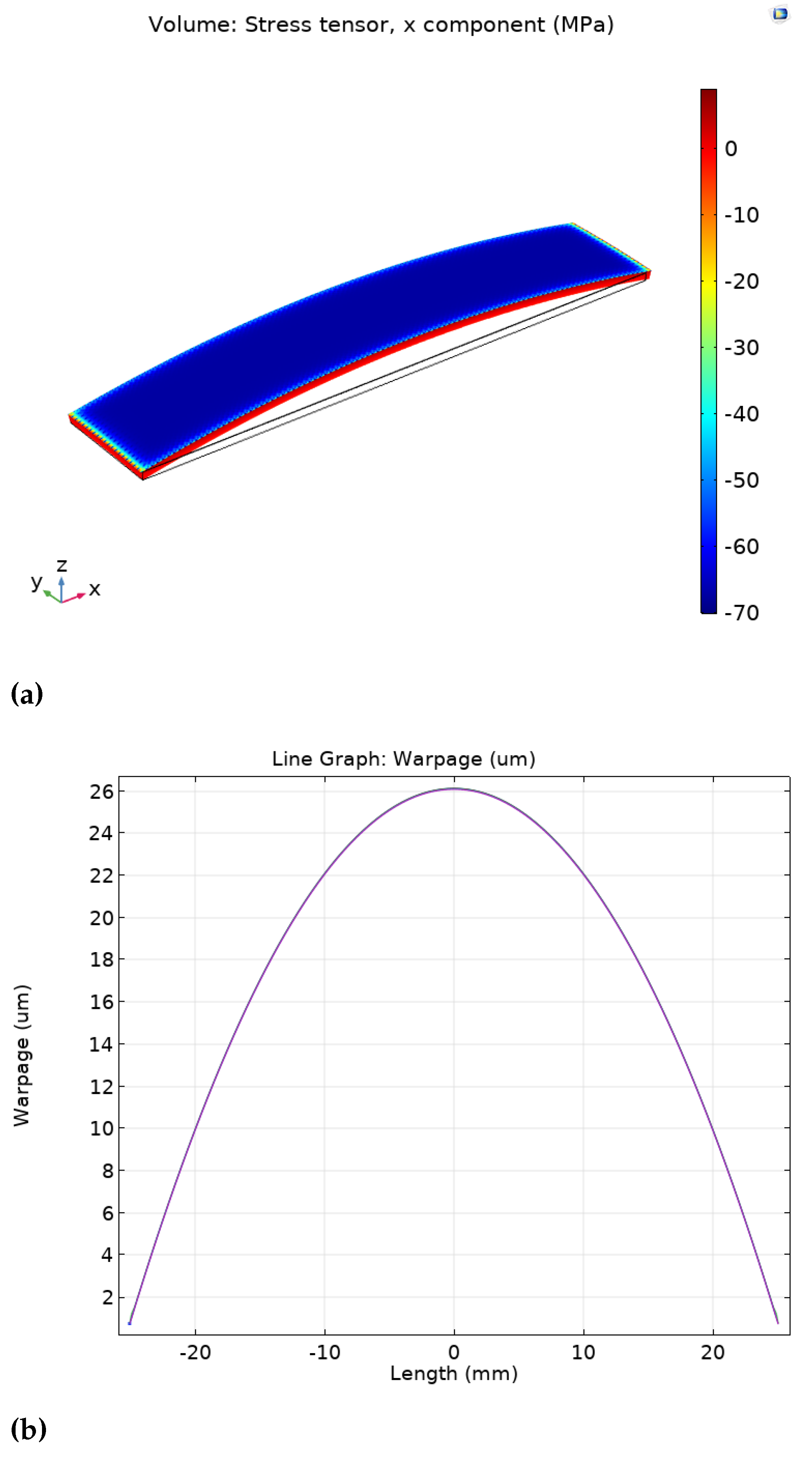
Material properties, reported in Table 1, are taken from internal material database based on material supplier data and nanoindentation tests to determin the Young modulus [31]. It is assumed material behavior as elastic and neglecting the temperature dependence. Linear elastic warpage and stress behavior is calculated with the customized FE model and two different literature approaches. One is derived from the Timoshenko theory for bi-metal thermostats [24], and the other is the Stoney equation [22], to calculate thermal warpage in thin film. Warpage results are benchmarked with experimental warpage observed in the second cycle during the first heating phase (50–90 C). Stress along x direction and warpage variation in temperature range 50–90 C are calculated with FEM, considering the system stress and strain free at 50 C. The results, shown in Figure 9, highlight stress is uniformly distributed on the strip, compressive on the copper side due to positive temperature variation. Warpage is correlated by means of a parabolic law with strip length.
The comparison between warpage and stress variation coming from considered methods is resumed in Table 2. FEM warpage is the closest with measurements and underestimates the experimental behavior of about 5%. Comparing between them the calculation methods, FEM predicts the highest warpage and highest stress, and it is the closest to the experimental measured warpage. The quite low difference between the Timoshenko and Stoney analytical approaches could be justified due to the fact that Timoshenko formula could be reduced assuming copper thickness much lower than silicon thickness. The difference observed in stress value can be addressed due to the fact that both the Timoshenko and Stoney approaches neglect the contribution of copper Poisson ratio, as explained in Section 4.1, while finite element model accounts this factor.
5. Conclusions
In this work, we studied the evolution of the deformation during the annealing process of ECD thick copper film (20 μm), measuring at different temperature the warpage of a wafer slice by means of dedicated optical technique. Analyses show an irreversible strain at a reference temperature (50 C) induced by the first heating cycle. Scanning electron microscopy analysis highlights that temperature profile induces grain growth, showing different in terms of grain dimension between samples heated at 150 and 250 . Exothermic process at around 160 is pointed out by differential scanning calorimetry: this evidence contributes to explain the detected grain size in samples heated at 150 and 250 Residual deformation depends strongly by maximum annealing temperature. Plateau does not affect the residual warpage. The deformation in elastic regime is reproduced with a preliminary linear FE model, which is a starting point to develop a more complete model to predict ECD warpage during entire annealing profile, considering the involved non-linearities and micro-structure modification that are pointed out by physical analysis.
Author Contributions
Conceptualization, G.S.; Data curation, A.S.; Investigation, M.C.; Methodology, M.C.; Supervision, S.M.O. and G.S.; Validation, A.S.; Writing—original draft, M.C. All authors have read and agreed to the published version of the manuscript.
Funding
This work was supported by the Università degli Studi di Catania (PIA.CE.RI. 2020-2022–Linea di Intervento 3 “Starting Grant,” MEPROSEMICON–Codice) under Grant 61722102147.
Institutional Review Board Statement
Not Applicable.
Informed Consent Statement
Not Applicable.
Data Availability Statement
Not Applicable.
Conflicts of Interest
The authors declare no conflict of interest.
References
- Nelhiebel, M.; Illing, R.; Detzel, T.; Wöhlert, S.; Auer, B.; Lanzerstorfer, S.; Rogalli, M.; Robl, W.; Decker, S.; Fugger, J.; et al. Effective and reliable heat management for power devices exposed to cyclic short overload pulses. Microelectron. Reliab. 2013, 53, 1745–1749. [Google Scholar] [CrossRef]
- Huang, R.; Robl, W.; Dehm, G.; Ceric, H.; Detzel, T. Disparate tendency of stress evolution of thin and thick electroplated Cu films at room temperature. In Proceedings of the 2010 17th IEEE International Symposium on the Physical and Failure Analysis of Integrated Circuits, Singapore, 5–9 July 2010; pp. 1–6. [Google Scholar] [CrossRef]
- Du, S.; Li, Y. Effect of Annealing on Microstructure and Mechanical Properties of Magnetron Sputtered Cu Thin Films. Adv. Mater. Sci. Eng. 2015, 2015, 1–8. [Google Scholar] [CrossRef] [Green Version]
- Calabretta, M.; Sitta, A.; Oliveri, S.M.; Sequenzia, G. An experimental-numeric approach to manufacture semiconductor wafer using thick copper front metallization. Int. J. Interact. Des. Manuf. IJIDeM 2020. [Google Scholar] [CrossRef]
- Wang, F.; Zhao, Z.; Nie, N.; Wang, F.; Zhu, W. Dynamic through-silicon-via filling process using copper electrochemical deposition at different current densities. Sci. Rep. 2017, 7, 46639. [Google Scholar] [CrossRef] [PubMed] [Green Version]
- Kauffman, J.; Gilbert, J.; Paterson, E. Multi-Physics Modeling of Electrochemical Deposition. Fluids 2020, 5, 240. [Google Scholar] [CrossRef]
- Chen, J.; Degryse, D.; Ratchev, P.; Wolf, I.D. Mechanical issues of Cu-to-Cu wire bonding. IEEE Trans. Compon. Packag. Technol. 2004, 27, 539–545. [Google Scholar] [CrossRef]
- Jeon, J.; Na, S.; Jeon, S.; Mo, M.; Kang, D.; Lim, K.; Kim, J. High reliability challenges with Cu wire bonding for automotive devices in the AEC-Q006. In Proceedings of the 2017 IEEE 67th Electronic Components and Technology Conference (ECTC), Orlando, FL, USA, 30 May–2 June 2017; pp. 1968–1973. [Google Scholar] [CrossRef]
- Chauhan, P.S.; Choubey, A.; Zhong, Z.; Pecht, M.G. (Eds.) Copper wire bonding. In Copper Wire Bonding; Springer: New York, NY, USA, 2014; pp. 1–9. [Google Scholar] [CrossRef]
- Bai, X.; Chang, B.; Du, D. Influences of material and structural factors on the stress conditions in Cu/low-k chips during Cu wire bonding. In Proceedings of the 2014 15th International Conference on Electronic Packaging Technology, Chengdu, China, 12–15 August 2014; pp. 441–446. [Google Scholar] [CrossRef]
- Auersperg, J.; Breuer, D.; Machani, K.V.; Rzepka, S.; Michel, B. FEA study of damage and cracking risks in BEoL structures under copper wirebonding impact. In Proceedings of the 2015 16th International Conference on Thermal, Mechanical and Multi-Physics Simulation and Experiments in Microelectronics and Microsystems, Budapest, Hungary, 19–22 April 2015; pp. 1–5. [Google Scholar] [CrossRef]
- Calabretta, M.; Guarnera, D.; Sitta, A.; Renna, M.; Sciuto, A.; D’Arrigo, G.; Oliveri, S.M.; Sequenzia, G. Mechanical characterization and modeling of different pad structures. In Proceedings of the 2020 21st International Conference on Thermal, Mechanical and Multi-Physics Simulation and Experiments in Microelectronics and Microsystems (EuroSimE), Cracow, Poland, 5–8 July 2020; pp. 1–5. [Google Scholar] [CrossRef]
- Cheng, G.; Xu, G.; Gai, W.; Luo, L. Influence of observed anelasticity of Cu on the wafer warpage evolution during thermal processes. In Proceedings of the 2018 19th International Conference on Electronic Packaging Technology (ICEPT), Shanghai, China, 8–11 August 2018; pp. 1119–1122. [Google Scholar] [CrossRef]
- Durand, C.; Klingler, M.; Coutellier, D.; Naceur, H. Power Cycling Reliability of Power Module: A Survey. IEEE Trans. Device Mater. Reliab. 2016, 16, 80–97. [Google Scholar] [CrossRef]
- Russo, S.; Bazzano, G.; Cavallaro, D.; Sitta, A.; Calabretta, M. Thermal analysis approach for predicting power device lifetime. IEEE Trans. Device Mater. Reliab. 2019, 19, 159–163. [Google Scholar] [CrossRef]
- Sitta, A.; Russo, S.; Bazzano, G.; Cavallaro, D.; Greco, G.; Calabretta, M. Numerical approach to predict power device reliability. In Proceedings of the 2018 13th International Conference on Design & Technology of Integrated Systems in Nanoscale Era (DTIS), Taormina, Italy, 9–12 April 2018; pp. 1–5. [Google Scholar] [CrossRef]
- Bayerer, R.; Herrmann, T.; Licht, T.; Lutz, J.; Feller, M. Model for Power Cycling lifetime of IGBT Modules—Various factors influencing lifetime. In Proceedings of the 5th International Conference on Integrated Power Electronics Systems, Nuremberg, Germany, 11–13 March 2008; pp. 1–6. [Google Scholar]
- Ciappa, M. Selected failure mechanisms of modern power modules. Microelectron. Reliab. 2002, 42, 653–667. [Google Scholar] [CrossRef]
- Calabretta, M.; Sitta, A.; Oliveri, S.M.; Sequenzia, G. Power Semiconductor Devices and Packages: Solder Mechanical Characterization and Lifetime Prediction. IEEE Access 2021, 9, 22859–22867. [Google Scholar] [CrossRef]
- Castoldi, L.; Morin, S.; Visalli, G.; Fukada, T.; Ouaknine, M.; Roh, E.; Yoo, W. Annealing characteristics of copper films for power device applications. In Thin Film Materials, Processes, and Reliability: Plasma Processing for the 100 Nm Node and Copper Interconnects with Low-k Inter-Level Dielectric Films: Proceedings of the International Symposium; The Electrochemical Society: Pennington, NJ, USA, 2003; Volume 2003, p. 330. [Google Scholar]
- Timoshenko, S. Analysis of bi-metal thermostats. Josa 1925, 11, 233–255. [Google Scholar] [CrossRef]
- Stoney, G.G. The tension of metallic films deposited by electrolysis. Proc. R. Soc. Lond. Ser. A Contain. Pap. Math. Phys. Character 1909, 82, 172–175. [Google Scholar] [CrossRef] [Green Version]
- Weidmann, D.; Dubois, G.; Hertl, M.; Chauffleur, X. Determination of strength of interface in packages based on an approach using coupling of experimental and modeling results. In Proceedings of the 2011 12th International Conference on Thermal, Mechanical & Multi-Physics Simulation and Experiments in Microelectronics and Microsystems, Linz, Austria, 18–20 April 2011; pp. 1–6. [Google Scholar] [CrossRef]
- Degrieck, J.; Van Paepegem, W.; Boone, P. Application of digital phase-shift shadow moiré to micro deformation measurements of curved surfaces. Opt. Lasers Eng. 2001, 36, 29–40. [Google Scholar] [CrossRef]
- Mancaleoni, A.; Sitta, A.; Colombo, A.; Villa, R.; Mirone, G.; Renna, M.; Calabretta, M. Copper wire bonding process characterization and simulation. In Proceedings of the CIPS 2020 11th International Conference on Integrated Power Electronics Systems, Berlin, Germany, 24–26 March 2020; pp. 1–4. [Google Scholar]
- Chaudhari, P. Grain growth and stress relief in thin films. J. Vac. Sci. Technol. 1972, 9, 520–522. [Google Scholar] [CrossRef]
- Ostrowicki, G.T.; Gurrum, S.P.; Nangia, A. Correlated model for wafer warpage prediction of arbitrarily patterned films. In Proceedings of the 2018 IEEE 68th Electronic Components and Technology Conference (ECTC), San Diego, CA, USA, 29 May–1 June 2018; pp. 2116–2120. [Google Scholar] [CrossRef]
- Bigl, S.; Wurster, S.; Cordill, M.; Kiener, D. Substrate-Influenced Thermo-Mechanical Fatigue of Copper Metallizations: Limits of Stoney’s Equation. Materials 2017, 10, 1287. [Google Scholar] [CrossRef] [PubMed] [Green Version]
- Vasudevan, M.; Johnson, W. Thermal Bending of a Tri-Metal Strip. Aeronaut. J. 1961, 65, 507–509. [Google Scholar] [CrossRef]
- Vasudevan, M.; Johnson, W. On multi-metal thermostats. Appl. Sci. Res. Sect. B 1961, 9, 420–430. [Google Scholar] [CrossRef]
- Sitta, A.; Renna, M.; Messina, A.A.; Mirone, G.; D’Arrigo, G.; Calabretta, M. Power module ceramic substrates: Mechanical characterization and modeling. In Proceedings of the 2020 21st International Conference on Thermal, Mechanical and Multi-Physics Simulation and Experiments in Microelectronics and Microsystems (EuroSimE), Cracow, Poland, 5–8 July 2020; pp. 1–5. [Google Scholar] [CrossRef]
Figure 1.
Temperature profile considered for annealing the samples and measuring the warpage in temperature.
Figure 1.
Temperature profile considered for annealing the samples and measuring the warpage in temperature.
Figure 2.
Experimental equipment TDM for warpage measurements.
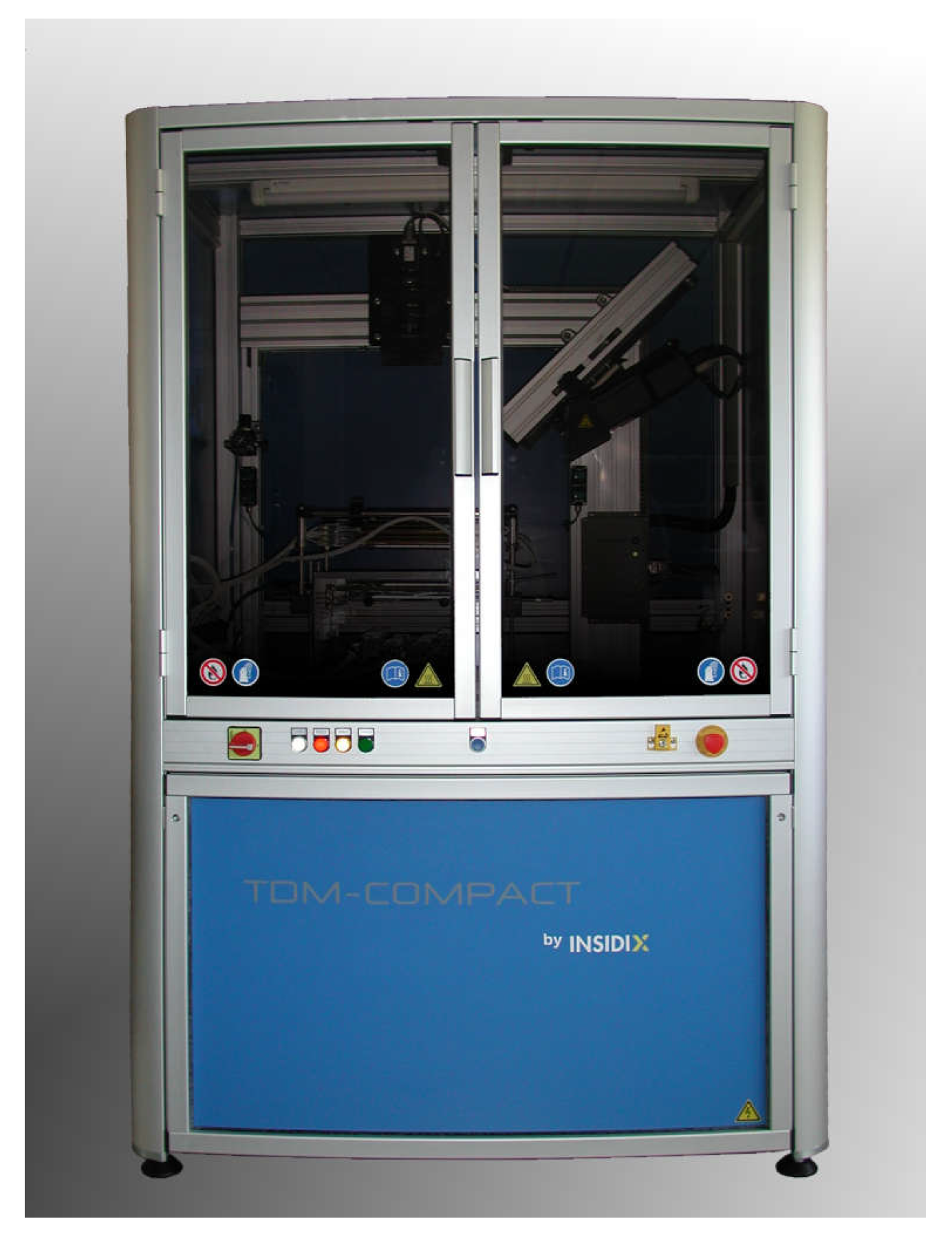
Figure 3.
Schematic of experimental setup for warpage measurement.
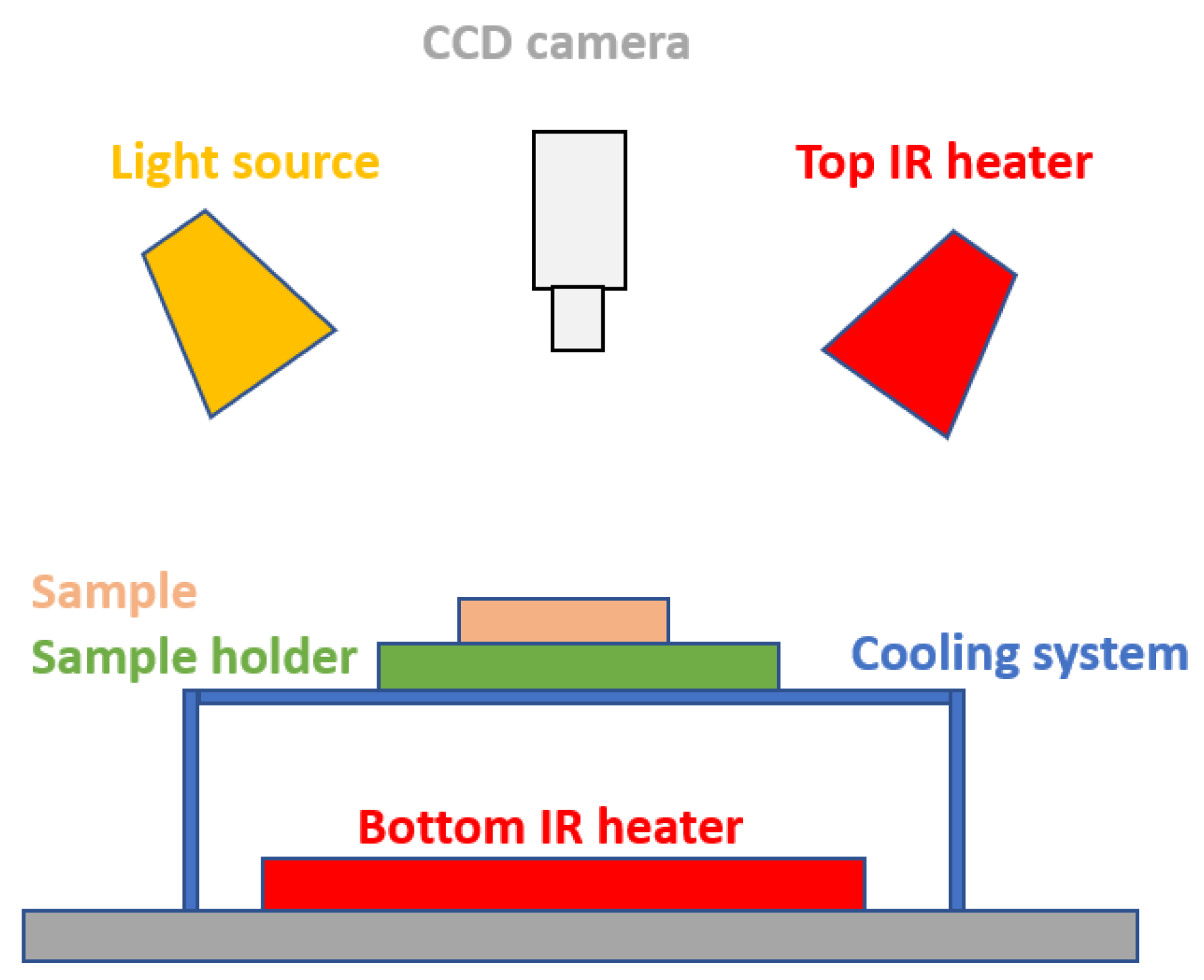
Figure 4.
Warpage maps at different temperature for temperature profile “W/o plateau”. On the right, the considered sign convention in Figure 5 is shown.
Figure 4.
Warpage maps at different temperature for temperature profile “W/o plateau”. On the right, the considered sign convention in Figure 5 is shown.
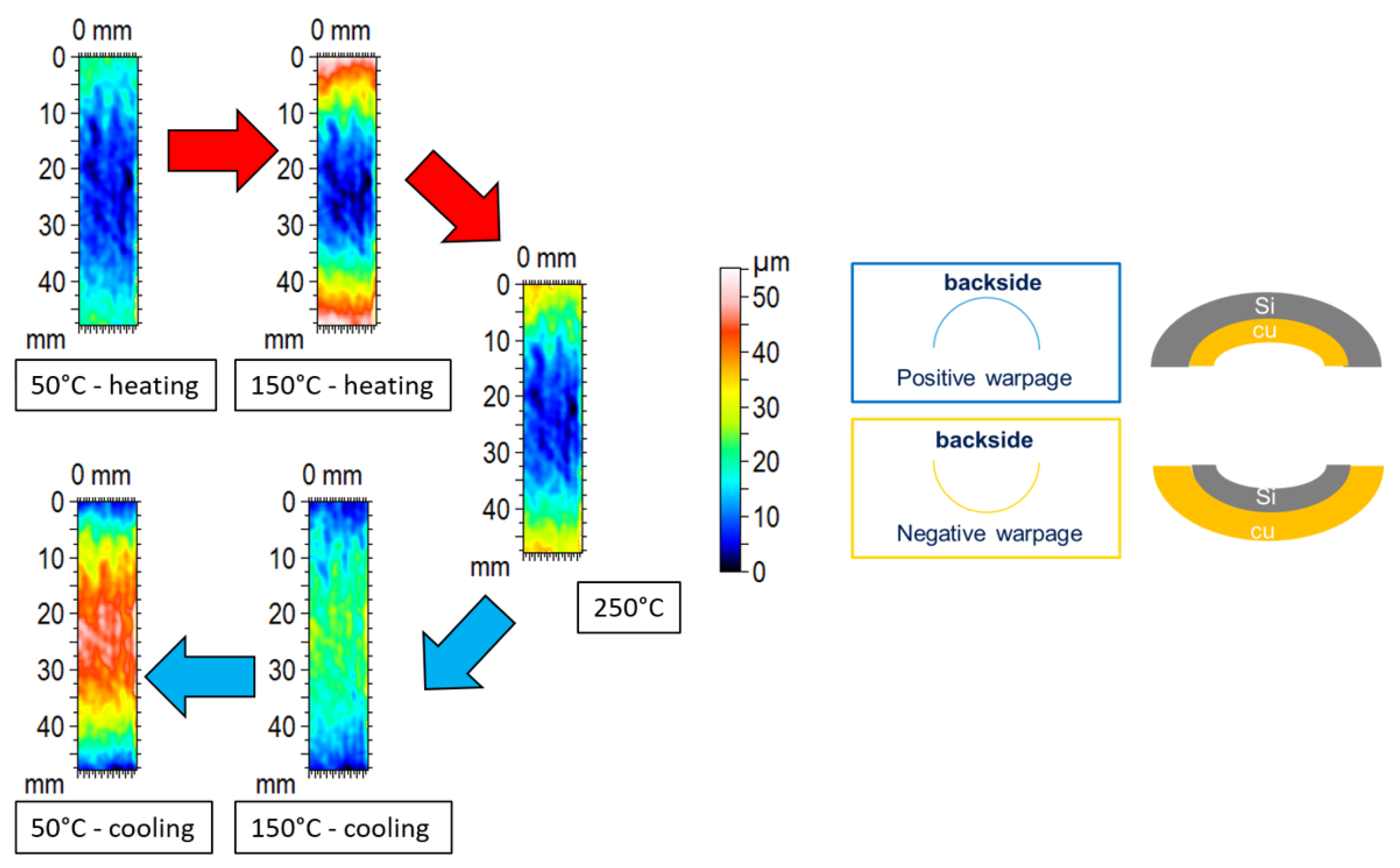
Figure 5.
Measured warpage during temperature profiles. Negative values are reached during the heating, while positive ones during the cooling phase. Dotted line represents the warpage versus temperature profile that occurred during a second temperature cycle.
Figure 5.
Measured warpage during temperature profiles. Negative values are reached during the heating, while positive ones during the cooling phase. Dotted line represents the warpage versus temperature profile that occurred during a second temperature cycle.
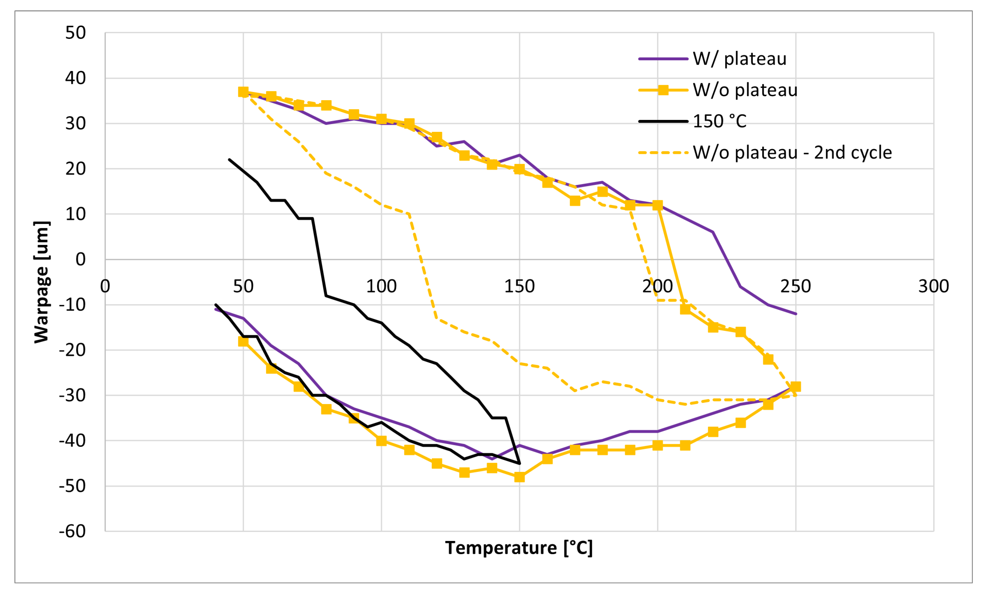
Figure 6.
Warpage profile at 150 C during heating for “W/o plateau” along cutline.
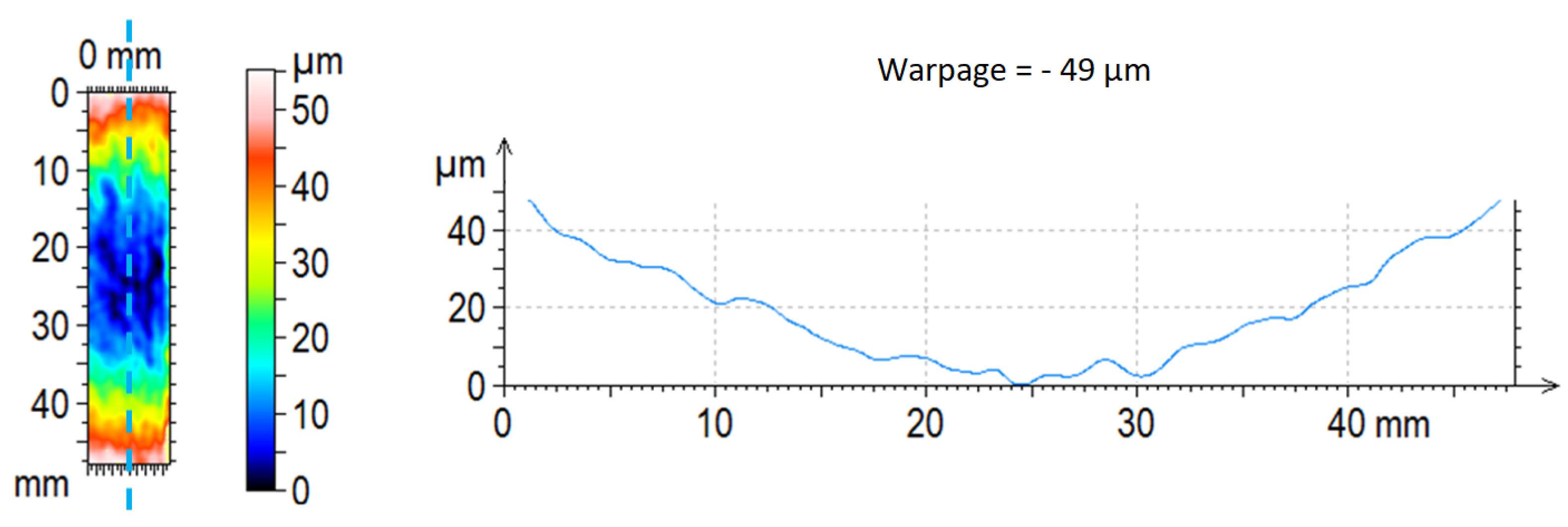
Figure 7.
DSC analysis on a thick copper samples which shows the starting of an exothermic process at about 160 .
Figure 7.
DSC analysis on a thick copper samples which shows the starting of an exothermic process at about 160 .

Figure 8.
Scanning electron microscopic on FIB-prepared samples without thermal treatment (a), heated at 150 (b), and at 250 (c). Grains can be distinguished by grey tonality.
Figure 8.
Scanning electron microscopic on FIB-prepared samples without thermal treatment (a), heated at 150 (b), and at 250 (c). Grains can be distinguished by grey tonality.
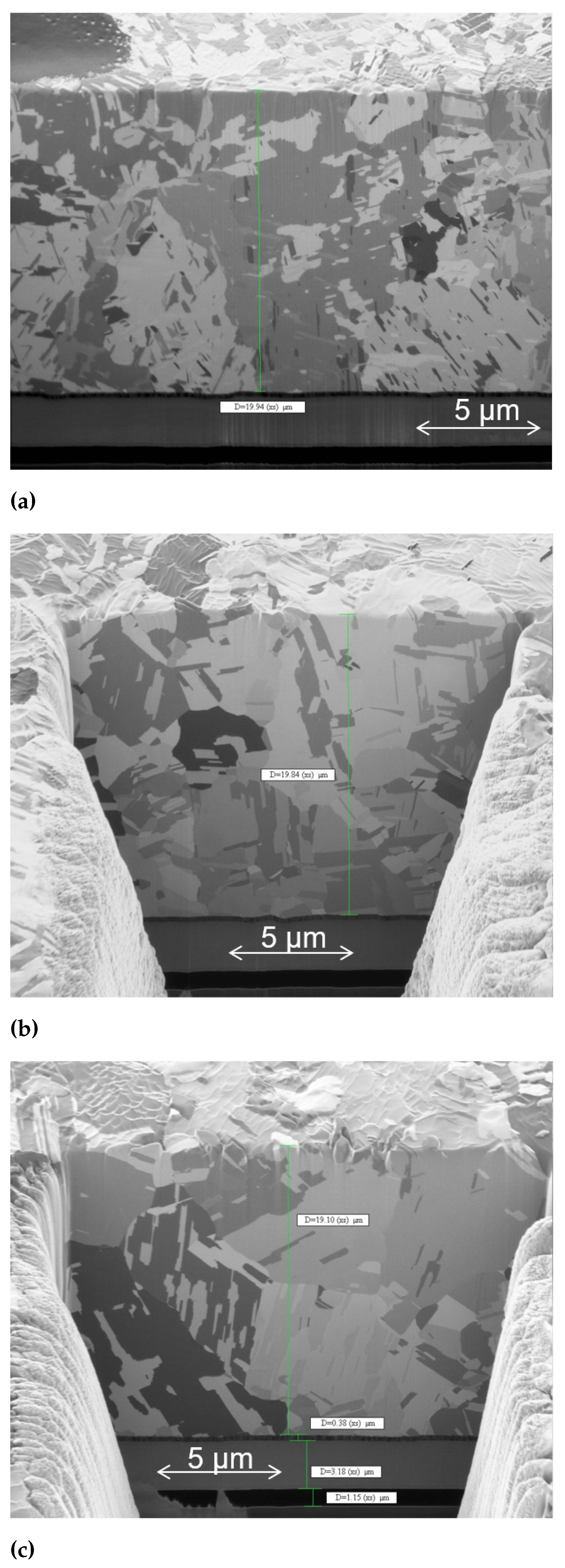
Figure 9.
Direction x-stress component (a) and warpage on z-direction computed by FEM (b).

Table 1.
Considered material data for simulation.
| Material | Young’s Modulus GPa | CTE ppm/K | Poisson Ratio |
|---|---|---|---|
| Silicon | 120 | 2.5 | 0.28 |
| Copper | 77.5 | 16.4 | 0.364 |
Table 2.
Simulation results (FEM) in terms of warpage and stress for temperature unit inside the linear heating region (50–90 C). It is reported, as reference, the analytic result coming from analytical approaches (Timoshenko and Stoney) and, as validation, the measured warpage (Experimental).
Table 2.
Simulation results (FEM) in terms of warpage and stress for temperature unit inside the linear heating region (50–90 C). It is reported, as reference, the analytic result coming from analytical approaches (Timoshenko and Stoney) and, as validation, the measured warpage (Experimental).
| Method | Experimental | FEM | Timoshenko | Stoney |
|---|---|---|---|---|
| Warpage [m/C] | 0.700 | 0.660 | 0.605 | 0.632 |
| Stress [MPa/C] | n.a. | 1.683 | 1.003 | 1.075 |
Publisher’s Note: MDPI stays neutral with regard to jurisdictional claims in published maps and institutional affiliations. |
© 2021 by the authors. Licensee MDPI, Basel, Switzerland. This article is an open access article distributed under the terms and conditions of the Creative Commons Attribution (CC BY) license (https://creativecommons.org/licenses/by/4.0/).
Share and Cite
MDPI and ACS Style
Calabretta, M.; Sitta, A.; Oliveri, S.M.; Sequenzia, G. Warpage Behavior on Silicon Semiconductor Device: The Impact of Thick Copper Metallization. Appl. Sci. 2021, 11, 5140. https://doi.org/10.3390/app11115140
AMA Style
Calabretta M, Sitta A, Oliveri SM, Sequenzia G. Warpage Behavior on Silicon Semiconductor Device: The Impact of Thick Copper Metallization. Applied Sciences. 2021; 11(11):5140. https://doi.org/10.3390/app11115140
Chicago/Turabian StyleCalabretta, Michele, Alessandro Sitta, Salvatore Massimo Oliveri, and Gaetano Sequenzia. 2021. "Warpage Behavior on Silicon Semiconductor Device: The Impact of Thick Copper Metallization" Applied Sciences 11, no. 11: 5140. https://doi.org/10.3390/app11115140
Note that from the first issue of 2016, this journal uses article numbers instead of page numbers. See further details here.