1. Introduction
Substrate integrated waveguide (SIW) is a technology enabling the design and manufacture of miniaturized waveguides. SIW technology mimics a dielectric waveguide that is implemented in a planar form due to the use of metallized vias, which form a waveguide in the employed substrate [
1]. In contrast with microstrip technology, SIW can be used to design radio-frequency devices with millimeter-wave frequencies (mmWave) [
2]. The main reason allowing this is the avoidance of radiation losses when the frequency increases, since the propagated wave is strongly confined in the substrate integrated waveguide. Therefore, losses in SIW devices are produced in the metal and mainly in the dielectric material, as is the case for microstrip technology where these losses are more significant. Apart from the above characteristics of SIW, it has the powerful advantage compared with conventional waveguide technology of enabling the cost-effective design of waveguide circuits.
In recent years, due to the mentioned advantages offered by SIW, many antennas and radio-frequency components such as filters or phase shifters have been reported using this technology [
3]. SIW antennas are of special interest due to the ease of integrating them as radiating elements in a complete system [
4]. Due to the low profile of SIW technology, a broad variety of SIW antennas have been conceived with both single and multiple layers. For instance, various researchers [
5,
6] have employed several SIW layers to create an antenna with a progressive aperture, where the substrate is drilled to improve the bandwidth and the gain. In [
7], a 60 GHz antenna array is presented where multiple SIW layers were fabricated on low-temperature co-fired ceramic (LTCC). In this case, the radiating element is an aperture backed by a cavity. Other antennas have been designed with layers of different types. For example, in [
8], the feeding layer is based on microstrip, while the radiating elements in the antenna array in [
9] were implemented in a metallic plate. Regarding SIW antennas with a single layer, examples can be found in [
10,
11], where the former used a corporate feeding network, and the latter did not. Moreover, SIW antennas in the literature apply different geometries and strategies to radiate the electric field that arrives at the antenna elements. Slotted antennas are preferred due to their easy implementation and the possibility of tuning the radiation in the design. In [
12], the impedance bandwidth of a cavity-backed slot antenna was improved by introducing a via hole. Nevertheless, the antenna operates at low frequency and it consists of a single antenna with low gain. Arrays of slot antennas that have also been reported are generally based on a backed cavity. There are examples where higher-order modes were excited in the backed cavity in order to operate in distinct frequency bands [
13,
14] or, conversely, the excited modes were close enough to a provide wide operating bandwidth [
15,
16]. Additionally, the relative orientations between slots can be adjusted in order to achieve the desired polarization [
17].
In this paper, we propose a cavity-backed antenna array whose radiating elements are double slots at millimeter-wave frequencies. We study the impact of introducing a single or a double slot in a cavity-backed antenna, finding that the double slot provides more control in the operating frequency band of the antenna array. A preliminary work on a cavity-backed antenna with two slots is presented in [
18]; however, the slots were used there to tune two very narrow bands around a center frequency of 10 GHz and the backed cavities were fed by cascade power dividers. In our work, a compact corporate feeding network is used and each backed cavity contains a subarray of 2 × 2 double slots, increasing the directivity of the complete antenna array. Additionally, the double slots are tuned to enhance the operating frequency band and achieve the desired directivity at mmWave bands. The proposed antenna represents a low-cost design with enhanced radiation performance for radiofrequency (RF) front-end hardware in future communications systems at millimeter-wave bands.
2. Design
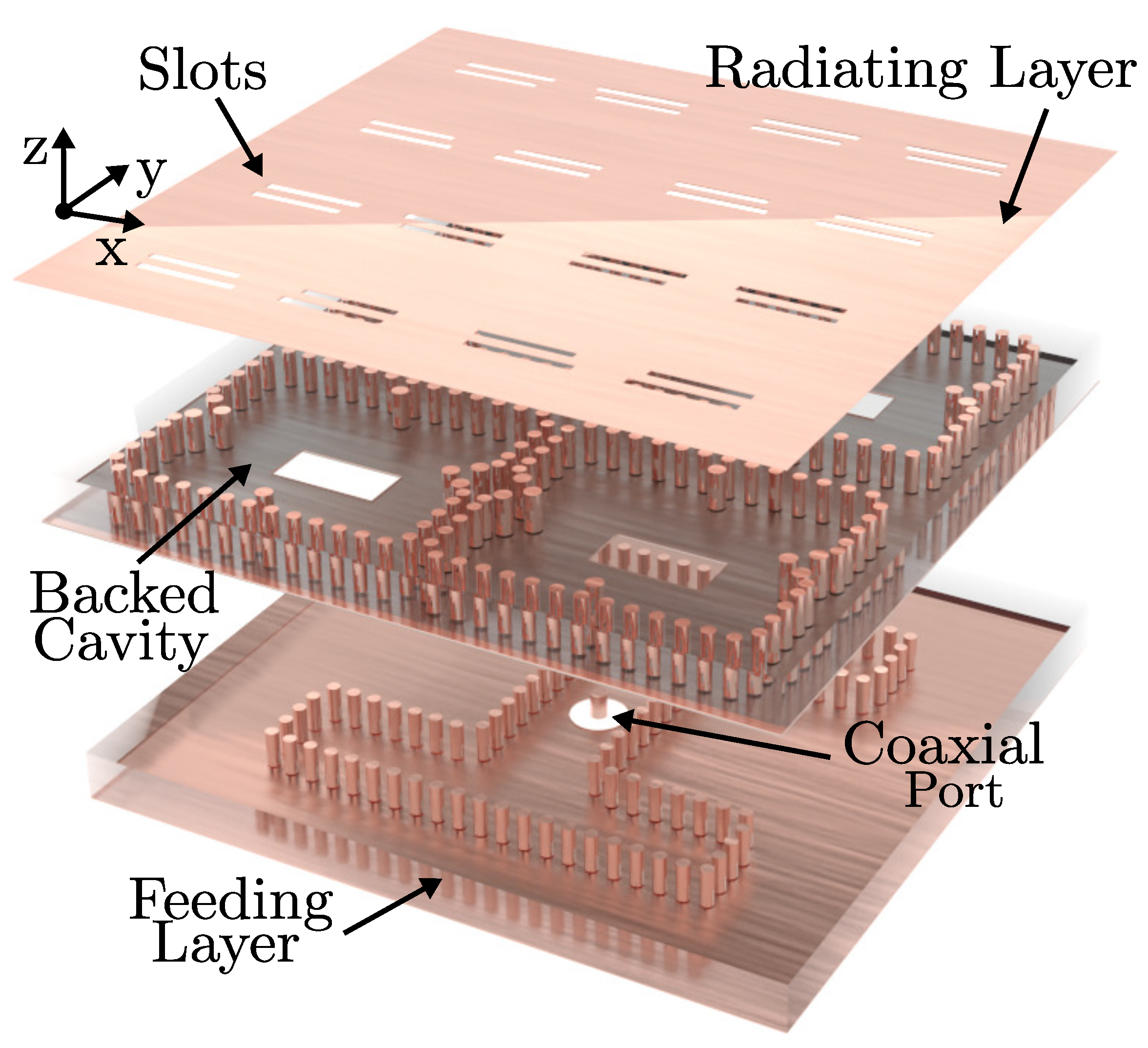
The complete antenna design is shown in
Figure 1. The antenna consists of two SIW layers, where the first one implements the feeding network and the second one contains the cavity-backed slot antennas. The antenna is fed by a coaxial port and then the feeding layer distributes the incoming power to the four inputs of the cavity-backed antennas. The second SIW layer, which is stacked atop the previous one, implements the backed cavities that allow the equal distribution of the power among the slots through the existence of a cavity mode. Each backed cavity contains a subarray of four double slots arranged in a 2 × 2 configuration. Therefore, the complete antenna is composed of 16 antenna elements configured in a square planar array to produce a pencil-shaped beam.
Each SIW layer is composed of a substrate coated on the upper and lower sides with copper. Inside each layer, metallized vias are inserted to implement the circuit based on substrate integrated waveguide. According to the design laws, these vias can simulate a metallized wall in order to confine the electromagnetic fields inside the substrate through the walls made by metallized via-holes (sides) and the two copper layers (top and bottom sides of the substrate). Equation (
1) specifies the maximum value of the periodicity of the metallic vias (
), which depends on the diameter of these metallic vias (
) [
19]. This diameter should be as small as possible but it must satisfy Equation (
2), which depends on the wavelength inside the substrate (
).
Values that do not satisfy the previous conditions would not allow a good confinement of the field, producing unacceptable values for the leaky-waves outside the structure. From a manufacturing point of view, mechanical limitations in the prototyping do not allow the distance between metallized via holes to be less than 0.3 mm, since lower values cause a failure in the manufacturing of the prototype. Thus, to prevent any of the above problems, the diameter of the vias and the period between them were set to 0.4 mm and 0.7 mm, respectively. This adjusts all values below the critical ones set by Equations (1) and (2) and the prototyping constraints.
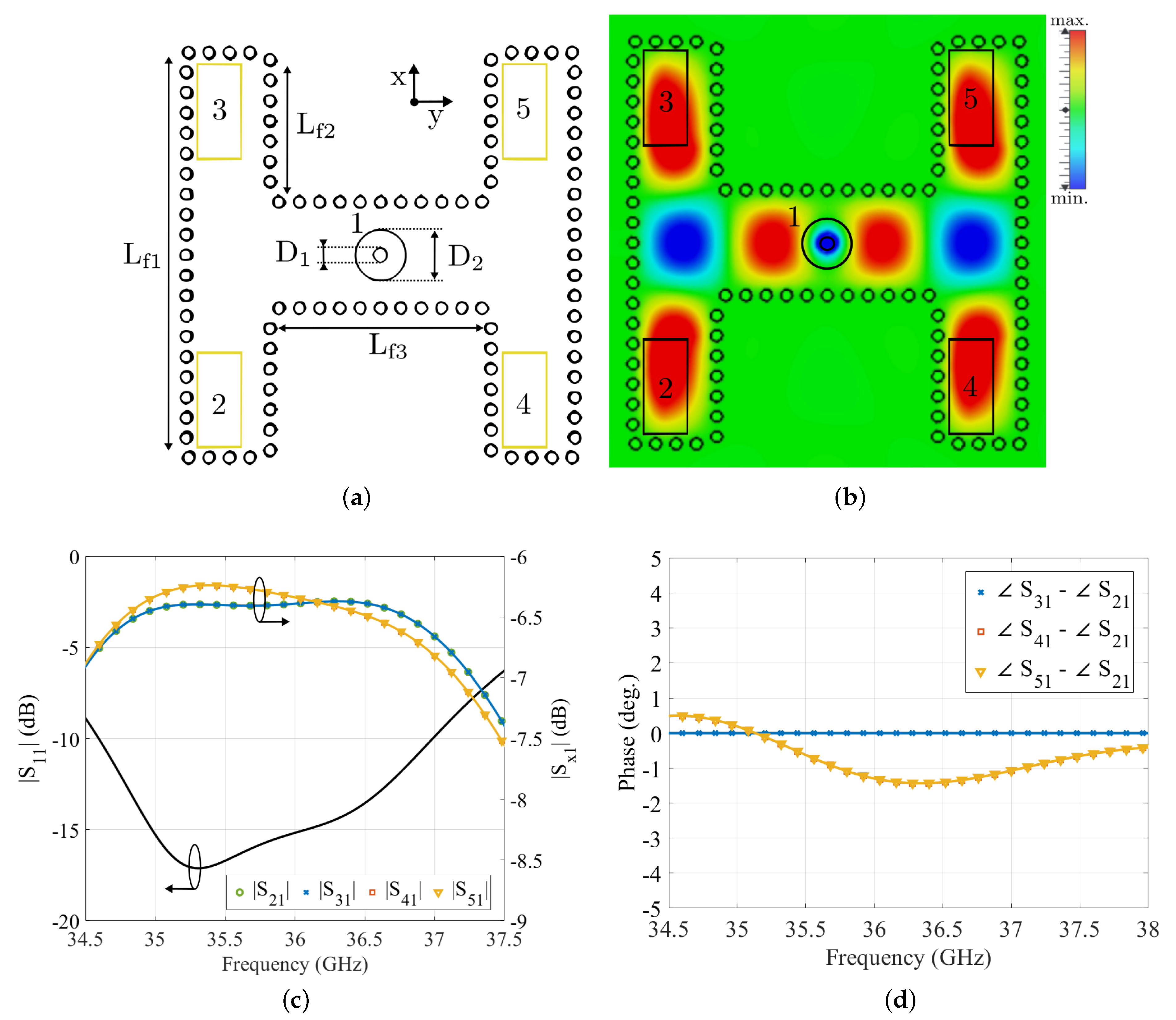
The planar view of the proposed corporate feeding network is illustrated in
Figure 2a. The feeding port (labeled as 1) is a coaxial line in which the inner conductor has a diameter D
1 and the outer conductor has a diameter D
2. These dimensions are imposed by a commercial connector used in the measurement setup [
20]. As shown in
Figure 2b, the incoming power is distributed to the T-type power dividers once it exits the coaxial line. In addition, the output fields from the feeding port are in phase, which is an advantage regarding the conventional E-plane waveguide power divider, which introduces a 180° phase shift between outputs. In the T-type power dividers placed after the feeding port, the power is split and directed to the rectangular coupling apertures (labeled as 2, 3, 4, and 5), as shown in
Figure 2a. The output waveguides of the T-type power divider is terminated at a short-circuited waveguide to favor the coupling to the rectangular apertures, which are the input ports to the backed cavities.
Figure 2a shows the dimensions of the substrate integrated waveguides that form the power dividers. Due to the proximity between the outputs of the power divider and the coupling apertures, the vias that form the waveguide turn toward the outputs favor the coupling without the need to use additional vias. This setup provides a compact corporate feeding network design. Another important design aspect of the proposed corporate feeding network is the location of the rectangular coupling apertures at the end of the waveguide. In order to ensure an in-phase feeding of the output ports of the feeding network, all the coupling apertures should on at the same side of the waveguide because the surface currents have the same direction. Otherwise, out-phase fields (phase difference of 180°) would be obtained at the output ports.
The described feeding network was designed and simulated in CST Microwave Studio. The simulations were performed for a relative electrical permittivity of the substrate of 3.35, a loss tangent of 0.0009, and a substrate thickness of 1.524 mm. All these characteristics correspond to the 4003C Rogers material, which is commercially available. The simulated results of the magnitude of the scattering parameters are shown in
Figure 2c. An input reflection coefficient below −10 dB was obtained from 34.5 to 37 GHz with equally distributed magnitude coefficients (around −6 dB). These transmission coefficients (|S
x1|) are slightly lower than expected due to the dielectric losses, since the loss tangent in simulation was set to 0.0009. The phase imbalance between output ports is illustrated in
Figure 2d. In this figure, a phase error lower than 2° is achieved. This is a very low value for the phase imbalance, being almost negligible in the radiation pattern of the antenna array.
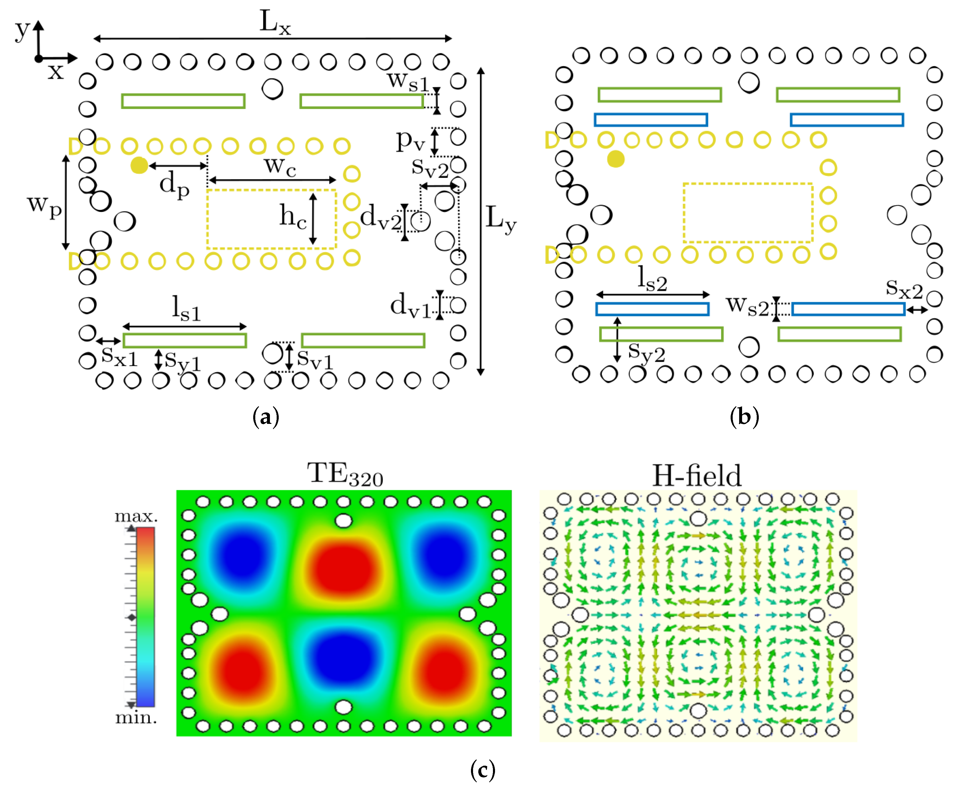
The second SIW layer of the antenna array contains the four backed cavities and the radiating slots. The backed cavity is fed at its bottom side with a rectangular coupling aperture with the same dimensions as the one described in the corporate feeding layer.
Figure 3a,b shows a planar view of the designed backed cavity where the rectangular coupling aperture, depicted using a yellow dashed line, is positioned at the center of the cavity to properly generate the fundamental mode of the cavity TE
320 (
Figure 3c). Some additional vias, whose dimensions are indicated by the parameters s
v1, d
v2, and s
v2, were introduced in the cavity design to improve the excitation of the cavity mode. This cavity mode is the one required to allow the radiation of the slots because the amplitude of the electric field and the orientation of the magnetic field produce an equal amplitude and in-phase radiation of the slots. In the designs illustrated in
Figure 3a,b, a difference exists between both planar views, which lies in the introduction of an additional slot in the double slot design (marked by a blue solid line). All the slots are placed near the corners of the backed cavity, as these are the locations at which the electromagnetic field favors slots radiation, as depicted in
Figure 3c. It is also necessary to consider that to enhance the power coupling between the substrate integrated waveguide (marked by solid yellow lines) and the cavity, it is required to introduce a coupling metallic via hole at a distance d
p from the rectangular coupling aperture. This coupling via is not introduced in the corporate feeding network depicted above, but it is employed in the design of a single cavity-backed antenna to reduce computational effort since the input port is located at the beginning of the substrate integrated waveguide (marked in yellow). It is important to remember that the vias that form the waveguide turns of the T-type power divider emulate the effect of this coupling via in the corporate feeding network design.
Once the cavity-backed antenna was designed, we compared the performance between the use of a single slot (
Figure 3a) and a double slot (
Figure 3b) as follows: First, a parametric study of the cavity-backed antenna using a single slot is shown in
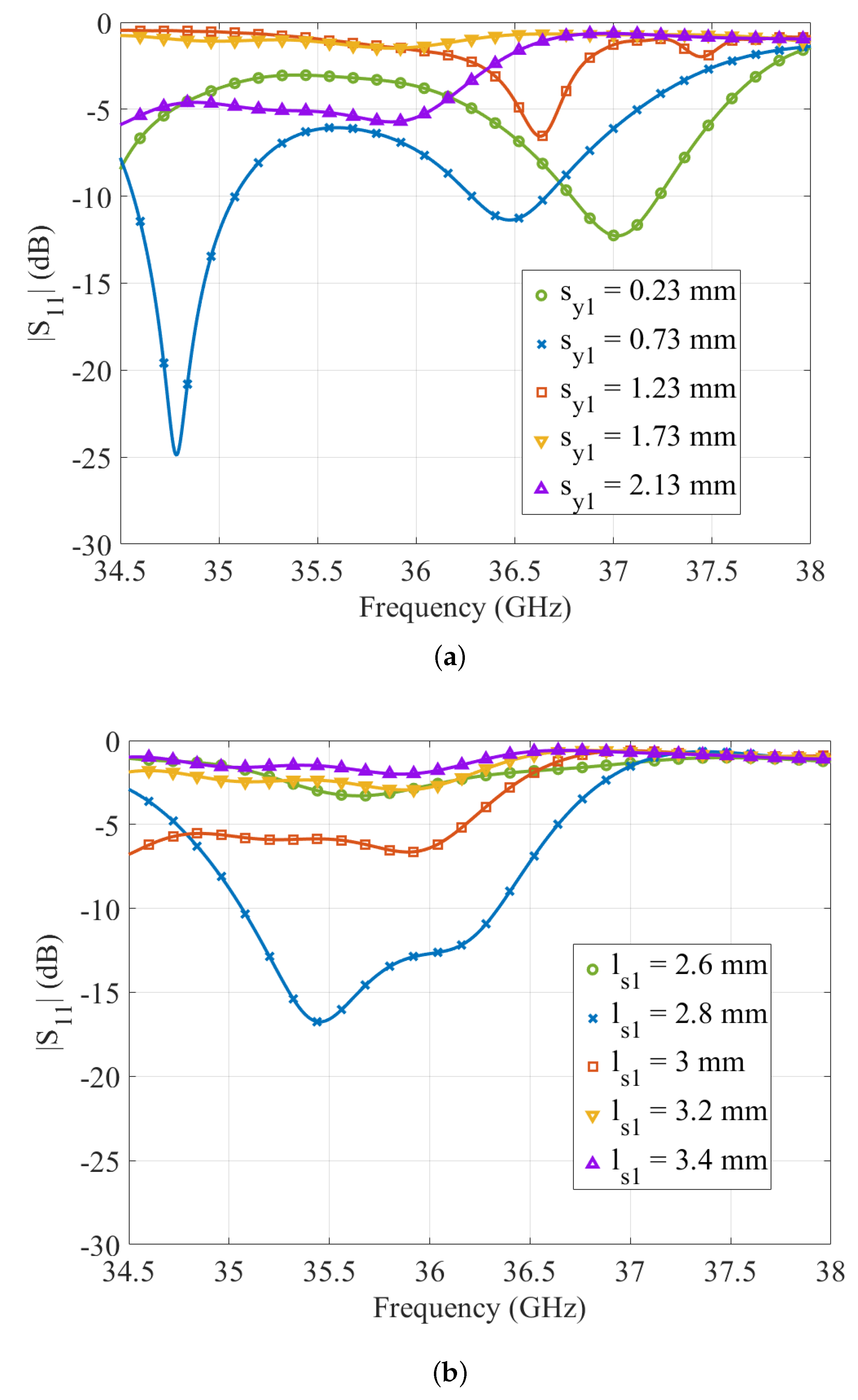
Figure 4. The modified parameters are s
y1, l
s1 and w
s1. The range of the selected parameters allows the assessment of the performance of the slots around the corners of the cavity-backed antenna. In each figure, the parameter under study is modified while maintaining the rest of the parameters as indicated in the caption of
Figure 3. The parameter s
y1 (
Figure 4a) represents the movement of the radiating slots in the
y direction. It can be observed that this is an important parameter for generating the operating frequency band. For s
y1 = 0.73 mm, a peak (resonance) in |S
11| appears around 35 GHz, but it has a narrow bandwidth. The length of the radiating slot l
s1 in
Figure 4b strongly defines the existence of a frequency bandwidth, since there is only one value that produces an impedance bandwidth below –10 dB. For other values of the slot length, no impedance bandwidth is observed. Finally, for the slot width w
s1, we performed a sweep of values (
Figure 4c). The slot width allows the fine tuning of the frequency bandwidths, providing an adjustment of the peaks depending on the target frequency ranges. In the figure, two separate peaks in |S
11| can be observed. So, by varying the width of the radiating slots, the center frequency can be tuned.
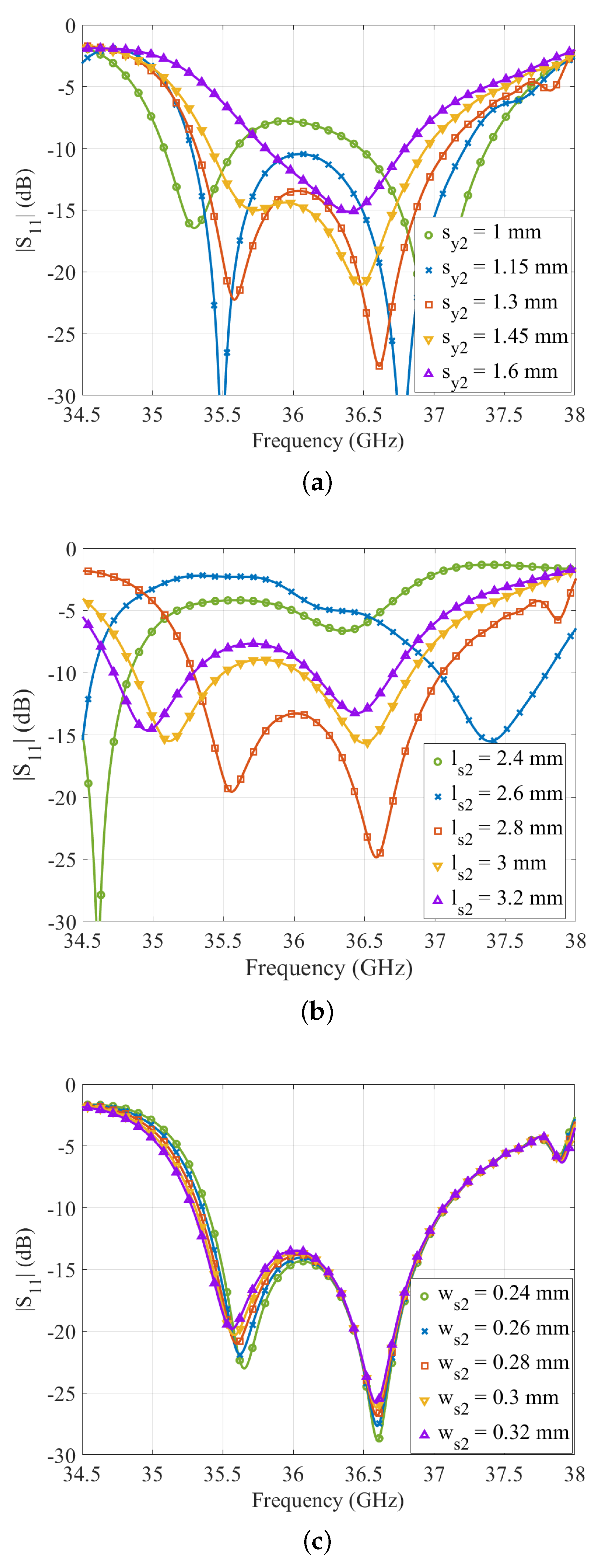
Figure 5 presents the parametric study of the second slot in the cavity-backed antenna with a double slot. For a fair comparison, the dimensions of the single slot are the same as the one in the results presented in
Figure 4. The dimensions under study for the second slot are the displacement in the
y direction (s
y2), slot length (l
s2), and slot width (w
s2). In
Figure 5a, the reflection coefficient is illustrated when s
y2 is modified. This parameter enables the control of the center frequencies of two narrow frequency bands. If it is modified properly, a greater impedance bandwidth can be achieved, as shown for s
y2 = 1.3 mm. The operating frequency range obtained has a bandwidth of 1.6 GHz, where most of the values are under −15 dB in the reflection coefficient. Compared with the previous results using a single slot in
Figure 4a, the great flexibility in the tuning of the operating frequency band(s) of the cavity-backed antenna when the double slot is introduced can be observed. The modification of the slot length l
s2 is displayed in
Figure 5b. In this case, the slot length produces a greater modification in the resonances of the cavity-backed antenna, providing better control than that observed for the single slot case (
Figure 4b). Lastly, the slot width w
s2 was varied. As observed for the single slot case, the slot width provides the fine tuning of the operating frequency band, as illustrated in
Figure 5c. Given these results and the comparison with the single slot case, the introduction of a second slot in the cavity-backed antenna provides more degrees of freedom in the design of the desired operating frequency bands.
3. Experimental Validation
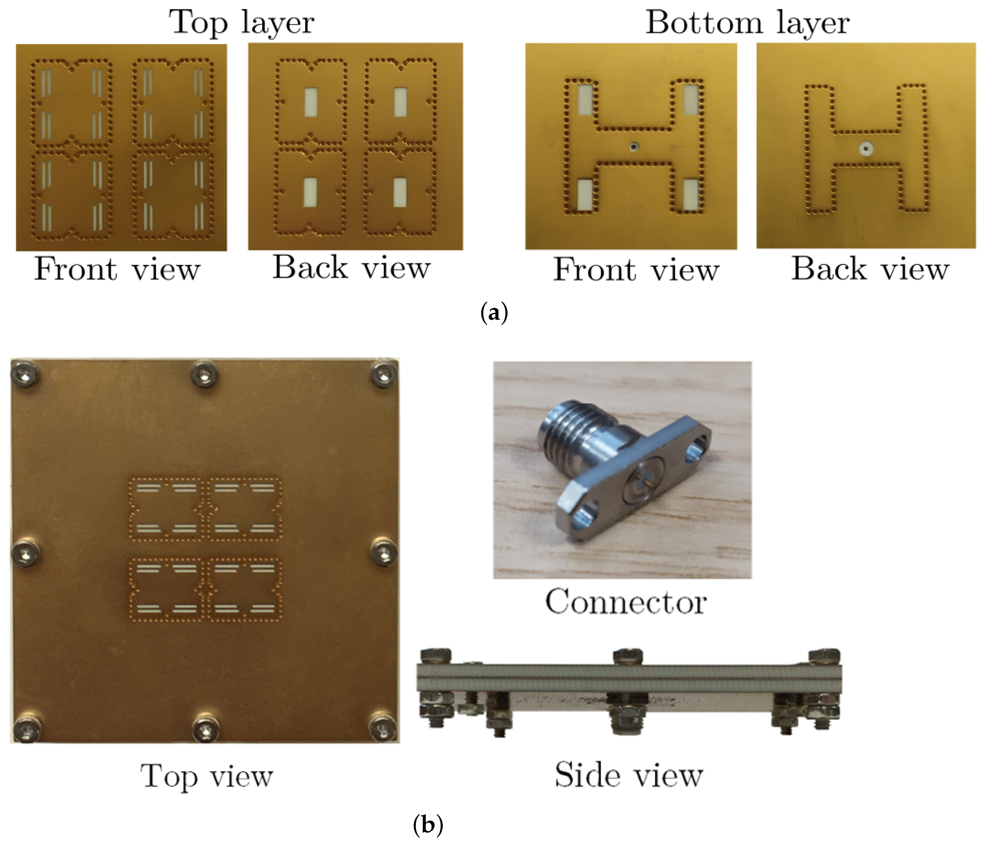
The design was experimentally validated using a complete prototype as detailed in
Figure 6. The prototype was formed by two layers, depicted in
Figure 6a. The bottom layer contained the corporate feeding network that included the one-to-four power divider and the coaxial feeding port. Notably, a hole was drilled at the center of the coaxial port in order to properly insert the inner conductor of the employed connector. The inner conductor of the commercial connector was precisely cut to obtain a length of 1.05 mm, which provided the expected impedance bandwidth. The top layer contained the four backed cavities and the radiating slots. The two layers were stacked and the assembly was fixed using mechanical pressure. Some details of the assembly are shown in
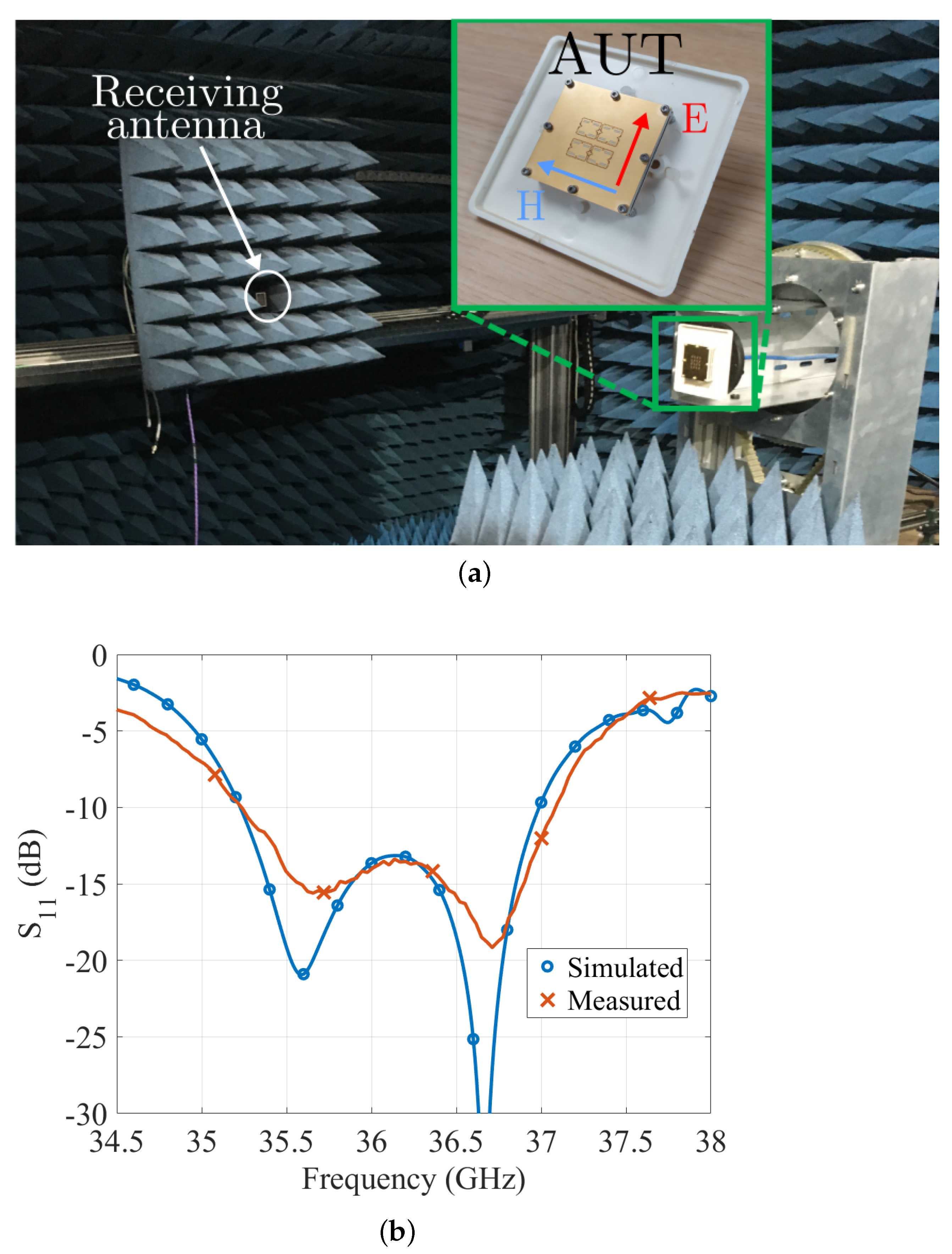
Figure 6b. The locations of the assembly screws were at the furthest part from the center of the plates to increase alignment accuracy. The antenna prototype was characterized inside the anechoic chamber of the SWAT Group at the University of Granada. Some details of the measurement setup and the antenna under test (AUT) position are shown in
Figure 7, where the E-plane and H-plane of the antenna are indicated. In the measurements, a transition from 1.85 to 2.92 mm was used since the ports of the vector network analyzer (VNA) R&S-ZVA67 were 1.85 mm and the antenna connector was 2.92 mm [
20]. An open-short-match (OSM) calibration was performed to remove the effects of the RF cable of the VNA as well as its 1.85 mm connectors. The 1.85 to 2.92 mm transition could not be included in the calibration setup, although its insertion losses were low (around 0.25 dB) and could therefore be neglected.
The antenna circuital matching measurement results are provided in
Figure 7b, which shows the measured reflection coefficient value of the complete prototype, as well as the simulated value for the sake of fair comparison. The samples acquired from the VNA were obtained each 32 MHz, representing a suitable sampling for measurement. The antenna provided a −10 dB bandwidth of around 1.6 GHz, with measured results agreeing with the expected ones from the simulation stage. This represents a good indicator of the proposed antenna assembly. If there had been any misalignment, the coefficient would have been affected, especially for misalignment in the
y direction of the antenna. The results show the double resonance that produces the desired frequency band due to the use of double slots in the cavity-backed antenna. Regarding the measurement results of the radiation patterns of the antenna,
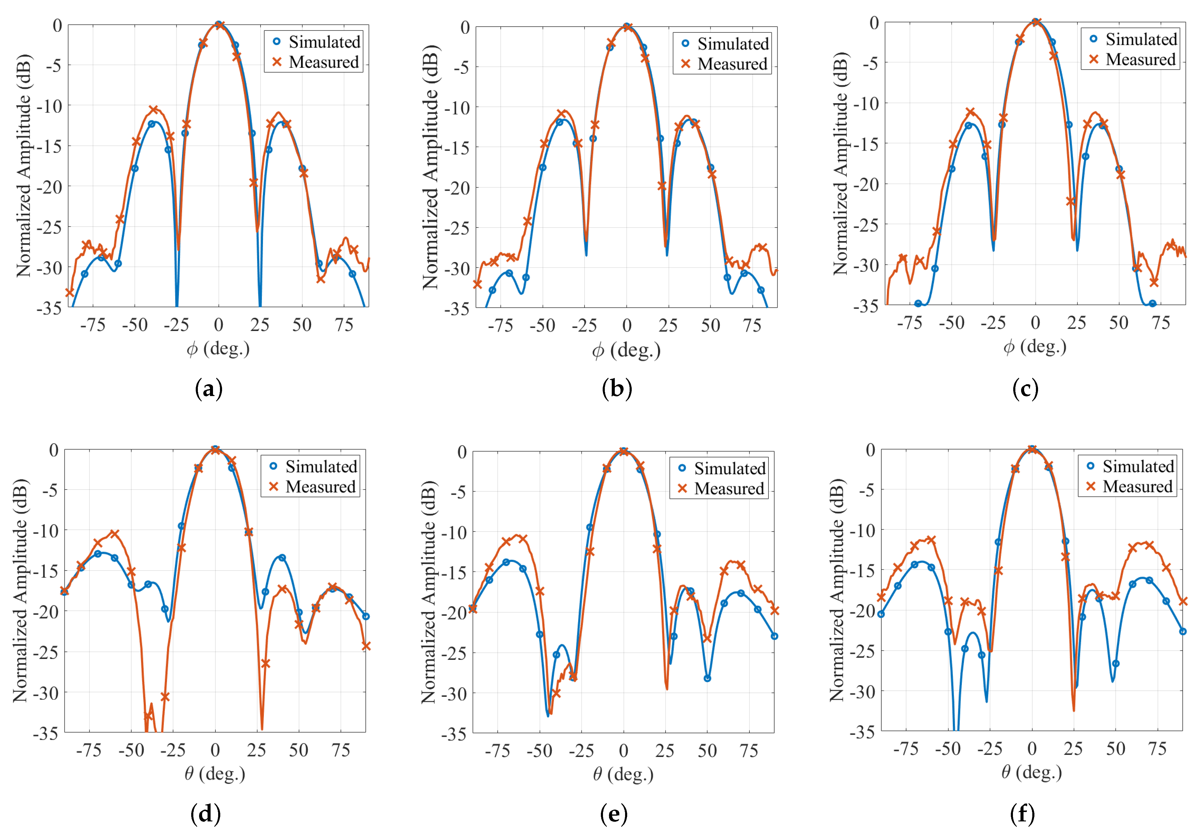
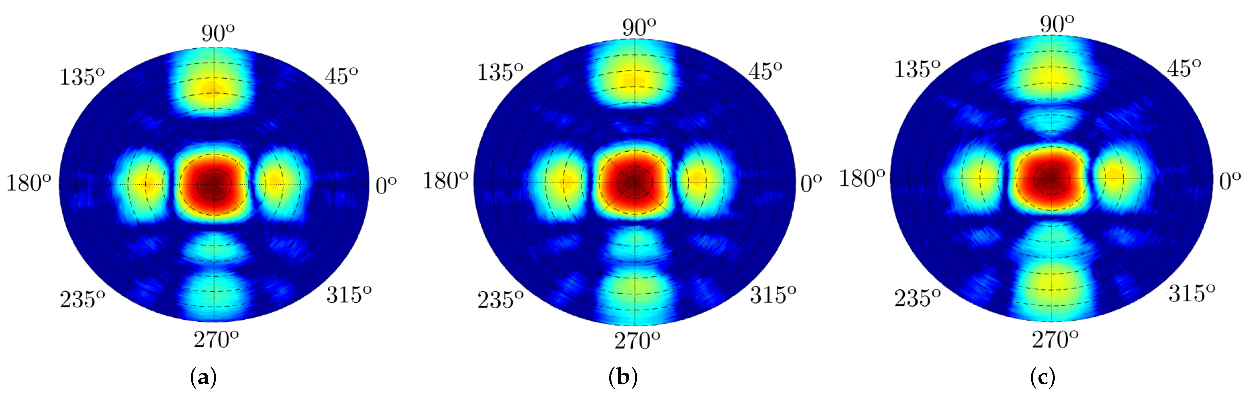
Figure 8 shows the simulated and measured H-plane and E-plane radiation patterns of the proposed SIW antenna at 35.4, 36.2, and 37 GHz, normalized to the steering direction. The radiation patterns in both planes match the expected pattern distribution. In the E-plane patterns, some side lobe levels are around 3 dB above the reference values.
Figure 9 depicts the measured 3D radiation patterns (spherical acquisition) of the proposed SIW antenna at 35.4, 36.2, and 37 GHz. The complete spherical radiation patterns match the expected performance of the array antenna since pencil-shape beams were produced in the whole operating frequency band.
Finally, directivity and gain measurements are provided in
Figure 10. The results were obtained for the main beam direction, that is, for azimuth (
) and elevation (
) angles equal to 0°. As shown, the simulated and measured gain values are in good agreement. The simulated and measured gain level is around 17 dBi and shows quite stable behavior in the desired working band (35.4 to 37 GHz). Notably, due to the transitions used for the receiving antenna and the AUT, some possible misalignments between the antennas, and slight modification of the phase center of the receiving horn with frequency, we estimates the error margin to be within 4.1%. The simulated directivity values are around 18 dBi, which means around 1.1 dB reduction due to the total efficiency of the antenna, which is directly linked to the dielectric losses. As cited in the Introduction, this is one of the main drawbacks of SIW antennas. Since the gain depends directly on the directivity and inversely on the losses, an increase in the losses leads to a reduction in the gain. However, this unfavorable effect may be compensated by obtaining a high-directivity antenna. In that case, even if the total power radiated is lower due to losses, this power would be concentrated in the desired direction.
The directive radiation pattern and the gain value achieved make this antenna suitable for directive communication systems in millimeter-wave bands. Additionally, due to the use of a corporate feeding network and cavity-backed antennas, the design of the antenna array allows the possibility of increasing the directivity and reducing the beamwidth in the steering direction by simply increasing the number of elements in the array. This array enlargement only requires stacking additional SIW corporate feeding network layers. For instance, an additional one-to-four corporate feeding network, which feeds four antenna arrays identical to the one presented in this paper, would permit the easy implementation of an array of 8 × 8 antenna elements. In addition, some challenges for the proposed design can be conceived, such as a wider operating band extension or modification using radiated polarization (the proposed design provides linear polarization).
Finally, in
Table 1, the proposed SIW antenna is compared with other slotted SIW antennas reported in the literature. The proposed antenna array design provides one of the highest working frequency bands compared with the reported antennas. Only the antenna proposed in [
14] presents an operating frequency band in the upper part of the Ka band; however, its relative bandwidth is smaller than that of the proposed design. Another remarkable feature of our antenna design is the maximum value of the gain achieved. This illustrates the efficiency provided by our antenna design even in frequency bands higher than those of some of the designs presented in other works with the same number of radiating elements [
11,
13].


 ,
, 


