Article

Electronically Tunable Mixed-Mode Universal Filter Employing a Single Active Block and a Minimum Number of Passive Components

by
Mohammad Faseehuddin
1,
Norbert Herencsar
2,*,
Musa Ali Albrni
3 and
Jahariah Sampe
3
1
Faculty of Engineering, Symbiosis Institute of Technology (SIT), Symbiosis International University (SIU), Pune, Maharashtra 412115, India
2
Department of Telecommunications, Brno University of Technology, Technicka 3082/12, 616 00 Brno, Czech Republic
3
Level 4 MINES Lab UKM, Institute of Microengineering and Nanoelectronics (IMEN), University Kebangsaan Malaysia (UKM), Bangi 43600, Selangor, Malaysia
*
Author to whom correspondence should be addressed.
Appl. Sci. 2021, 11(1), 55; https://doi.org/10.3390/app11010055
Submission received: 7 October 2020 / Revised: 27 November 2020 / Accepted: 2 December 2020 / Published: 23 December 2020
(This article belongs to the Section Electrical, Electronics and Communications Engineering)

Abstract

:

Featured Application

Active analog filters are widely used for frequency duplexing in radar and radio communication systems, impedance matching in power amplifiers, anti-aliasing in data converters and in many other areas.

Abstract

A recently developed active building block, namely Voltage Differencing Extra X Current Conveyor (VD-EXCCII), is employed in the design of multi input single output (MISO), electronically tunable mixed-mode universal filter. The filter provides low pass (LP), high pass (HP), band pass (BP), band reject (BR) and all pass (AP) responses in current-mode (CM), voltage-mode (VM), trans-impedance-mode (TIM) and trans-admittance-mode (TAM). The filter employs a single VD-EXCCII, three resistors and two capacitors. Additionally, a CM single input multi output (SIMO) filter can be derived from the same circuit topology by only adding current output terminals. The attractive features of the filter include: (i) the ability to operate in all four modes, (ii) the tunability of the Q factor independent of pole frequency, (iii) the low output impedance for the VM filter, (iv) the high output impedance current output for CM and TAM filters and (v) no requirement for double/negative input signals (voltage/current) for response realization. The VD-EXCCII and its layout is designed and validated in Cadence Virtuoso using 0.18 µm pdk from Silterra Malaysia with a supply voltage of ±1.25 V. The operation of the filter is examined at the 8.0844 MHz characteristic frequency. A non-ideal parasitic and sensitivity analysis is also carried out to study the effect of process and components spread on the filter performance.

1. Introduction

The current-mode (CM) active building blocks (ABBs) are widely employed in designing universal frequency filters. The CM ABBs exhibits greater linearity, wide bandwidth, simple structure, low power consumption and enhanced dynamic range [1,2,3,4,5]. Extensive number of filter topologies using CM ABBs can be found in the literature. However, the majority of the previously proposed filters can work only in single mode of operation i.e., CM, voltage-mode (VM), trans-impedance-mode (TIM) or trans-admittance-mode (TAM) [1,2,3,5]. In present-day intricate signal processing systems, the interaction between CM and VM circuits is required. This task can be accomplished by TAM and TIM filters that not only perform signal processing, but also provide interfacing between VM and CM systems [6,7,8,9,10]. The development of mixed-mode universal filters that can provide low pass (LP), high pass (HP), band pass (BP), band reject (BR) and all pass (AP) filter responses in CM, VM, TAM and TIM modes of operation are best suited for the task.
Numerous exemplary mixed-mode filter structures have been developed that employ different variants of the CM ABBs [8,9,10,11,12]. The filters can be segregated in two broad categories single input multi output (SIMO) and multi input single output (MISO) type. The MISO filter configuration is one of the most sought after. The filters can be compared on many criteria, some important measures of comparison are: (i) number of ABBs employed, (ii) number of passive components needed, (iii) employment of all grounded passive components, (iv) no requirement for resistive matching except for AP response, (v) provision to control quality factor (Q) independent of the center frequency, (vi) ability to provide all five filter responses in all four modes of operation, (vii) low output impedance for VM mode, (viii) availability of explicit current output in CM and TAM modes, (ix) no requirement for double/negative input signals (voltage/current), (x) inbuilt tunability and (xi) test frequency. A detailed comparison of the state-of-the-art MISO filters with the proposed design is presented in Table 1 [6,7,8,9,10,11,12,13,14,15,16,17,18,19,20,21,22,23,24,25,26,27,28,29,30,31,32,33,34,35,36,37,38,39] and Table 2 [7,9,12,13,19,20,24,25,26,27,29,37,38,39,40,41] It can be inferred from the tables that the filter structures in [6,7,8,9,10,11,12,13,15,16,17,18,19,20,21,22,23,24,26,28,29,30,31,32,33,34,35,36,37,38,39] employ more than one ABB. The designs in [6,7,10,12,22,28,29,30,36,37,39,41] use more than five passive components. The filter structures proposed by [6,7,9,10,11,12,13,18,19,21,24,25,27,30,32,33,36,39] do not provide frequency control independent of quality factor. The filter structures [6,8,9,11,13,14,15,16,18,21,23,25,26,27,28,32,34,35,41] do not provide all five filter responses in VM, CM, TAM and TIM operation. The filter structures [6,7,10,11,12,14,16,22,25,27,28,29,30,34,36,37,39,41] lack inbuilt tunability property. In addition, only four mixed mode filter structures [14,25,27,40] employing a single ABB can be currently found in the literature. Moreover, among single ABBs based mixed mode filters only [40] provides all five filter responses in all four modes of operation. Furthermore, the design in [40] does not provided VM response at low impedance node. It can be deduced from the literature survey that a limited number of mixed-mode filters are available, and to fill this technological void, additional novel mixed-mode filter structures are needed.
In the literature, numerous CM ABBs can be found, each having its own merits. In this research, the Voltage Differencing Extra X Current Conveyor (VD-EXCCII) is introduced and utilized in the design of mixed-mode filter. The proposed VD-EXCCII can be considered a universal ABB, as it can realize many popular and widely employed CM ABBs as special case. The proposed VD-EXCCII can realize second generation current conveyor (CCII), voltage differencing current conveyor (VDCC), differential difference current conveyor (DDCC), voltage differencing transconductance amplifier (VDTA), voltage differencing buffered amplifier (VDBA), current backward transconductance amplifier (CBTA) and operational transconductance amplifier (OTA) by proper interconnection of its input and output terminals, thereby making it an inherently universal ABB. This will allow designers to employ VD-EXCCII instead of using each separate ABBs to test their designs, thus reducing the cost and time to market. The filter design requires a single VD-EXCCII, two capacitors and three resistors. The striking features of the proposed filters are: (i) employment of single active block (VD-EXCCII), (ii) ability to work in all four modes of operation, (iii) provision for inbuilt tunability, (iv) the filter enjoy low active and passive sensitivities. Moreover, the filter enjoy all (iv–x) properties mentioned in Table 2. The design simulation of the VD-EXCCII is done in Cadence Virtuoso using Silterra Malaysia 0.18 µm PDK. The post-layout simulation results are in good agreement with the theoretical predictions.

2. Voltage Differencing Extra X Current Conveyor (VD-EXCCII)

The proposed Voltage Differencing Extra X current conveyor (VD-EXCCII) is derived by connecting extra X second generation current conveyor (EXCCII) [
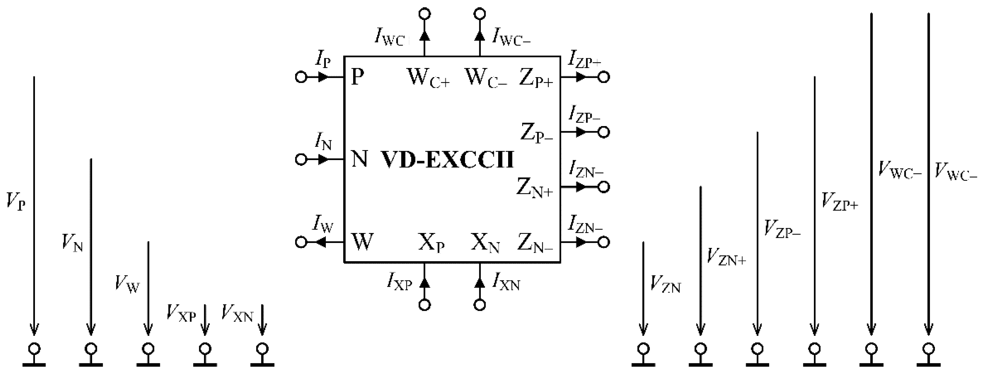
42] and operational transconductance amplifier (OTA). The first stage comprises of OTA followed by the CCII with two current input terminals. The developed active element has characteristics of CCII and tunable OTA in one structure. The voltage-current (V–I) characteristics of the developed VD-EXCCII are presented in Equations (1)–(4) and the block diagram is presented in Figure 1.
I W = I W C + = I W C = g m 1 ( V P V N )
V X P = V X N = V W
I X P = I Z P + = I Z P
I X N = I Z N + = I Z N
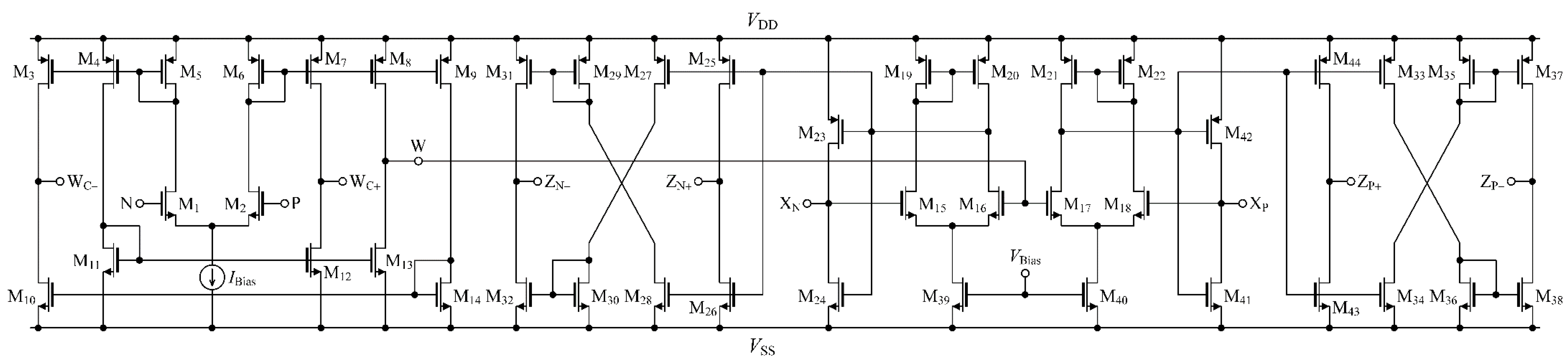
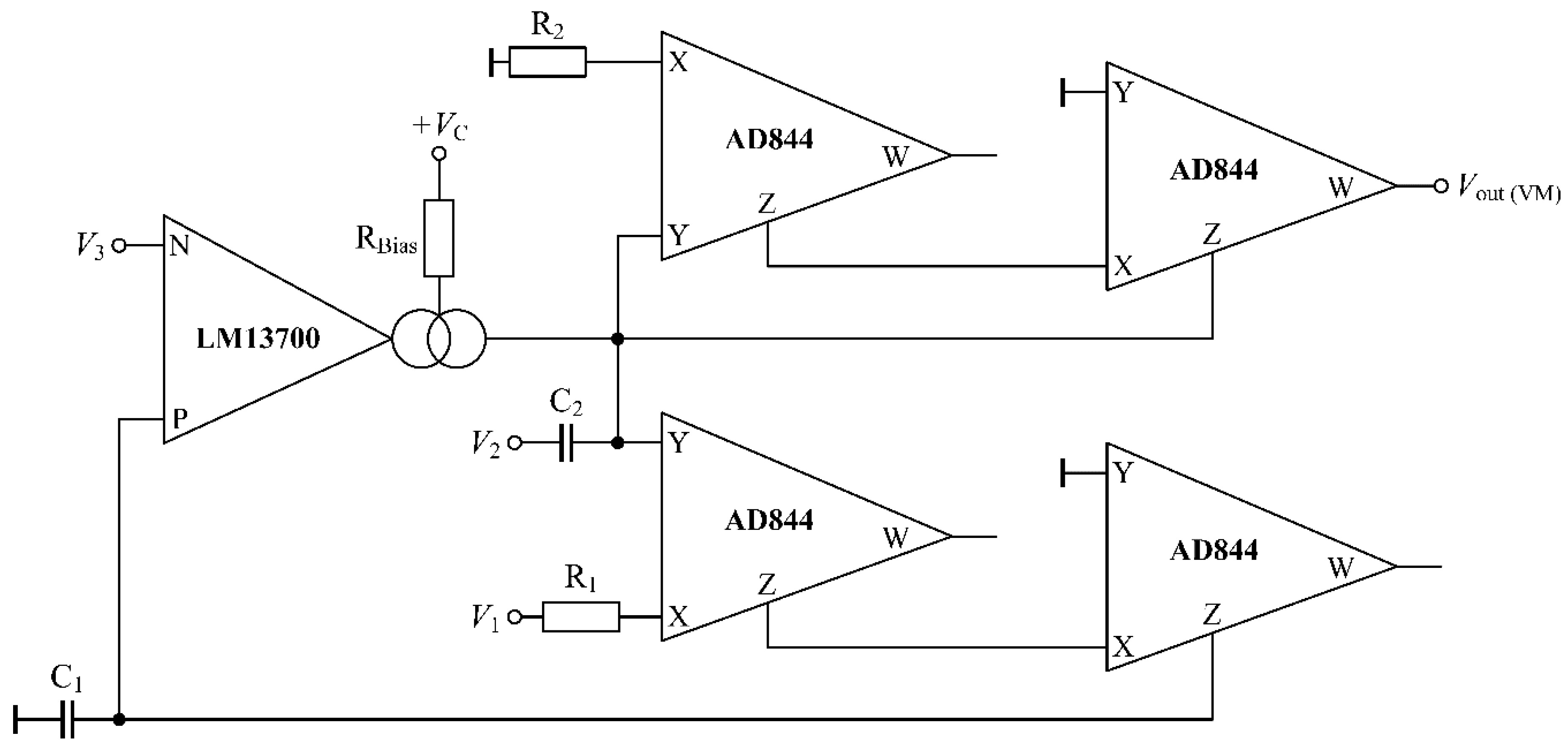
The CMOS implementation of VD-EXCCII is given in Figure 2. The first stage consists of OTA MOS transistors (M1–M14). The output current of the transconductor depends on the voltage difference ( V P V N ) . Assuming that all transistors are operating in saturation region and the transistors (M1–M2) have equal width to length ratio, the output current is given by:
I W = I W C + = I W C = g m 1 ( V P V N ) = ( 2 I B i a s K i ) ( V P V N )
where the transconductance parameter K i = µ C o x W 2 L , (i = 1, 2), W is the effective channel width, L is the effective length of the channel, C o x is the gate oxide capacitance per unit area and µ is the carrier mobility.
The second stage is made up of hybrid voltage and current followers (M15–M44). The voltage developed at node W is transferred to nodes X P and X N . In the same way the input current from X P node is transferred to Z P + and Z P . Furthermore, the input current from X N node is transferred to Z N + and Z N . The current flowing in the Z N and Z P terminals are independent of each other. The class AB output stage is utilized in the output stage, as it is suitable for low voltage operation and better dynamic range [2]. The current and voltage reference circuits available in the literature [43] can be employed to generate the IBias and VBias for the circuit.
The small signal analysis yields the expression relating V W ,   V X P   and   V X N . The analysis is carried out for the differential stage formed by transistors ( M 15 M 24 ,   M 39 M 42 ) . The voltage transfer ratio between the W and X P node can be derived as given in Equation (6).
α P = V X P V W = r 039 r 040 r 039 + r 040 ( g m 39 + g m 40 ) r 0 p 2 g m 18 r 039 r 040 r 039 + r 040 ( g m 39 + g m 40 ) r 0 p 2 g m 17 + 1 g m 18 g m 17
where r 0 p = r 017 / / r 021 , r 0 is the output resistance of the MOS transistor and g m i is the transconductance of the MOS transistor M i . Similarly, the voltage transfer gain α N is computed as:
α N = V X N V W g m 15 g m 16
The current transfer ratios are derived as given in Equations (8) and (9):
β P = I Z P I X P = r 041 r 042 r 041 + r 042 ( g m 41 + g m 42 ) r 041 r 042 r 041 + r 042 ( g m 41 + g m 42 ) + R Z L O A D r 039 r 040 r 039 + r 040 ( g m 39 + g m 40 ) r 039 r 040 r 039 + r 040 ( g m 39 + g m 40 ) + R X L O A D ( g m 41 + g m 42 ) ( g m 39 + g m 40 )
β N = I Z N I X N     ( g m 25 + g m 26 ) ( g m 23 + g m 24 )
The terminal resistance of X N and X P terminals is calculated as given in Equations (10) and (11). The Z P + , Z N + and W C + resistance are presented in Equations (12)–(14).
R X P = 1 r 039 r 040 r 039 + r 040 ( g m 39 + g m 40 ) r 0 p 2 g m 18     2 r 0 p g m 18 ( g m 39 + g m 40 )
R X N     2 r 0 n g m 15 ( g m 23 + g m 24 )
where r 0 p = r 017 / / r 021 and r 0 n = r 016 / / r 020 .
R Z P + = r 039 r 040 r 039 + r 040
R Z N + = r 025 r 026 r 025 + r 026
R W C + = r 08 r 013 r 08 + r 013
The Z P + , Z N + and W C + node impedances are found to be high given by the parallel output resistance of the MOS transistors.

3. Proposed Electronically Tunable Mixed-Mode Universal Filter

The proposed MISO mixed mode filter is presented in Figure 3. It provides all five filter responses in VM, TAM, TIM and CM modes of operation. The minimum component filter employs a single VD-EXCCII, three resistors and two capacitors. The main attributes of the filter are: (i) use of a single active element, (ii) employment of only five passive components, (iii) no need for capacitive matching condition, (iv) availability of VM output from low impedance terminal, (v) availability of TAM and CM output from high impedance terminals, (vi) no requirement for negative/double input signals for response realization, (vii) inbuilt tunability of Q independent of frequency and (viii) in TIM mode, the filter gain can be adjusted without affecting ω 0 and Q.

3.1. Operation in VM and TAM

In this mode of operation, all input currents ( I 1 I 3 ) are set to zero. The input voltages ( V 1 V 3 ) are applied as per the sequence given in Table 3. The filter transfer functions and expression for pole frequency and quality factor are given in Equations (15)–(18):
V o u t = V 1 g m 1 R 2 g m 1 R 2 R 1 s C 1 V 3 + s 2 C 1 C 2 R 1 R 2 V 2 s 2 C 1 C 2 R 1 R 2 + s C 1 R 1 + g m 1 R 2
I o u t ( T A M ) = 1 R 2 V 1 g m 1 R 2 g m 1 R 2 R 1 s C 1 V 3 + s 2 C 1 C 2 R 1 R 2 V 2 s 2 C 1 C 2 R 1 R 2 + s C 1 R 1 + g m 1 R 2
ω 0 = g m 1 C 1 C 2 R 1
Q = R 2 C 2 g m 1 C 1 R 1
The Equations (17) and (18) imply that when the frequency is varied, the quality factor of the filter will be slightly affected. The frequency can be tuned without affecting the quality factor if g m 1 and R 1 are varied simultaneously such that the product ( R 1 · g m 1 ) remains constant. The resistor can be realized using a MOS [44] transistor, making it easily tunable.

3.2. Operation in CM and TIM

In CM mode, the input voltages are set to zero. The input currents ( I 1 I 3 ) are applied according to Table 4 to obtain CM and TIM responses.
The filter transfer functions are given in Equations (19) and (20):
I o u t = ( s 2 C 1 C 2 R 1 R 2 + g m 1 R 2 ) I 2 + s C 1 R 1 I 3 + g m 1 R 1 I 1 s 2 C 1 C 2 R 1 R 2 + s C 1 R 1 + g m 1 R 2
In TIM mode, the gain of the filter can be varied without disturbing the Q and ω 0 of the filter by varying the value of R 3 , as in the transfer function, R 3 is common to all the responses:
V o u t ( T I M ) = R 3 [ ( s 2 C 1 C 2 R 1 R 2 + g m 1 R 2 ) I 2 + s C 1 R 1 I 3 + g m 1 R 1 I 1 s 2 C 1 C 2 R 1 R 2 + s C 1 R 1 + g m 1 R 2 ]
Additionally, the CM SIMO filter shown in Figure 4 is derived from the proposed mixed mode filter by adding additional current output terminals without changing the core topology. All passive components are grounded in CM SIMO configuration. The filter requires a single VD-EXCCII, two resistors and two capacitors, all grounded. The resistor R 3 is not required. since it is needed only to obtain the TIM response. The attractive features of the derived SIMO CM filter include (i) use of single active element, (ii) employment of only three grounded passive components, (iii) no need for passive components matching condition, (iv) low input impedance, (v) high output impedance and (vi) inbuilt tunability.
The filter transfer functions are given in Equations (21)–(25). Expression for pole frequency and quality factor will be same as that of mixed mode MISO filter given by Equations (17) and (18).
I L P I I N = g m 1 R 2 s 2 C 1 C 2 R 1 R 2 + s C 1 R 1 + g m 1 R 2
I H P I I N = s 2 C 1 C 2 R 1 R 2 s 2 C 1 C 2 R 1 R 2 + s C 1 R 1 + g m 1 R 2
I B P I I N = s C 1 R 2 s 2 C 1 C 2 R 1 R 2 + s C 1 R 1 + g m 1 R 2
The BR and AP response can be obtained by simply summing the LP, HP and BP currents: I B R = I H P + I L P and I A P = I H P + I L P + I B P .
I N P I I N = g m 1 R 2 s 2 C 1 C 2 R 1 R 2 s 2 C 1 C 2 R 1 R 2 + s C 1 R 1 + g m 1 R 2
I A P I I N = g m 1 R 2 s 2 C 1 C 2 R 1 R 2 + s C 1 R 2 s 2 C 1 C 2 R 1 R 2 + s C 1 R 1 + g m 1 R 2

4. Non-Ideality and Sensitivity Analysis

4.1. Non-Ideal Gain and Sensitivity Analysis

The non-ideal effects that influences the response of the VD-EXCCII are the frequency-dependent non-ideal current ( α P / N ,   α P / N ), voltage ( β P / N ) and transconductance transfer (γ, γ ) gains. These non-ideal gains result in a change in the current and voltage signals during transfer leading to undesired response. Taking into account the non-ideal gains, the V–I characteristics of the VD-EXCCII in (1–4) will be modified as follows: I W = 0 , V X P = β P V W , V X N = β N V W , I Z P + = α P I X P , I Z P = α P I X P , I Z N + = α N I X N , I Z N = α N I X N ,   I W = I W C + = γ g m 1 ( V P V N ) , I W C = γ g m 1 ( V P V N ) , where β ( P ,   N ) = 1 ε v ( P , N ) , α P = 1 ε i P , α N = 1 ε i N , γ = 1 ε g m 1 and γ = 1 ε g m 1 . Here, ε v ( P , N )   ( | ε v ( P , N ) |   «   1 ) denote voltage tracking errors, ε i P , ε i N ( | ε i P | ,   | ε i N |   «   1 ) denote current tracking errors and ε g m 1 , ε g m 1 ( | ε g m 1 | ,   | ε g m 1 |   «   1 ) denote transconductance errors of the VD-EXCCII.
The non-ideal analysis considering the effect of non-ideal current, voltage and transconductance transfer gains is carried out for VM, CM, TAM and TIM configurations to see its effect on the transfer function, f0 and Q of the proposed filters. The modified expressions of the filter transfer functions, f 0 and Q for the MISO/ SIMO configurations are presented in Equations (26)–(31):
V o u t ( V M - M o d e ) = [ s 2 C 1 C 2 R 1 R 2 V 2 Υ g m 1 s C 1 R 1 R 2 V 3 + α N Υ g m 1 R 1 R 2 V 1 s 2 C 1 C 2 R 1 R 2 + α P β P s C 1 R 1 + β N α N Υ g m 1 R 2 ]
I o u t ( T A M - M o d e ) = α P β P R 2 [ s 2 C 1 C 2 R 1 R 2 V 2 Υ g m 1 s C 1 R 1 R 2 V 3 + α N Υ g m 1 R 1 R 2 V 1 s 2 C 1 C 2 R 1 R 2 + α P β P s C 1 R 1 + β N α N Υ g m 1 R 2 ]
I o u t ( C M - M o d e ) = [ α P [ s 2 C 1 C 2 R 1 R 2 + β P α P s C 1 R 1 + β N α N Υ g m 1 R 2 ] I 2 + α P β P α P s C 1 R 1 I 2 + α P β P s C 1 R 1 I 3 + α P β P α N Υ g m 1 R 1 I 1 ] s 2 C 1 C 2 R 1 R 2 + α P β P s C 1 R 1 + β N α N Υ g m 1 R 2 ]
V o u t ( T I M - M o d e ) = R 3 [ α P [ s 2 C 1 C 2 R 1 R 2 + β P α P s C 1 R 1 + β N α N Υ g m 1 R 2 ] + α P β P α P s C 1 R 1 I 2 + α P β P s C 1 R 1 I 3 + α P β P α N Υ g m 1 R 1 I 1 ] s 2 C 1 C 2 R 1 R 2 + α P β P s C 1 R 1 + β N α N Υ g m 1 R 2 ]
f 0 = 1 2 π β N α N Υ g m 1 C 1 C 2 R 1
Q = R 2 α P β P β N α N Υ g m 1 C 2 C 1 R 1
The sensitivities of ω 0 and Q with respect to the non-ideal gains and passive components are given below:
S g m 1 ω 0 = S α N ω 0 = S β N ω 0 = S γ ω 0 = S C 1 ω 0 = S C 2 ω 0 = S R 1 ω 0 = 1 2
S g m 1 Q = S α N Q = S β N Q = S γ Q = S C 1 Q = S C 2 Q = S R 1 Q = 1 2
S R 2 Q = S α P Q = S β P Q = 1
The sensitivities are low and have absolute values not higher than unity.

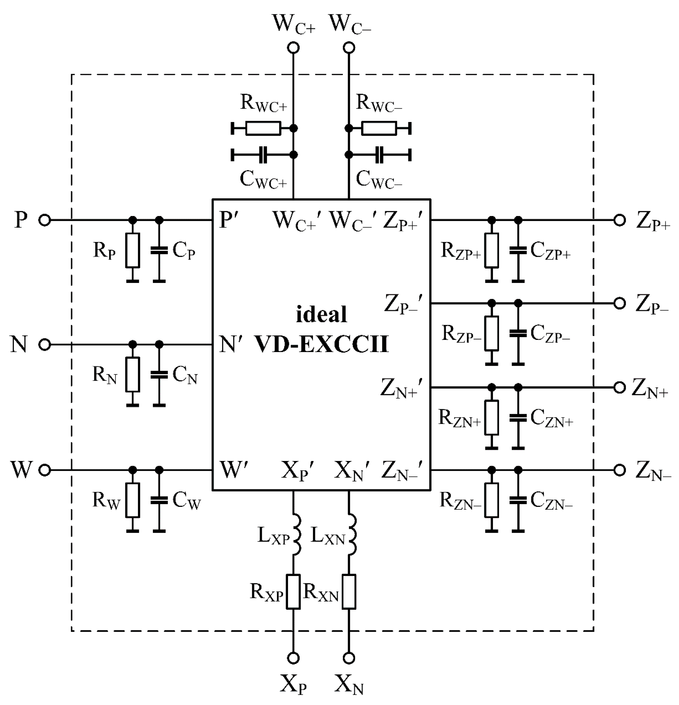
4.2. Non-Ideal Parasitic Analysis

The non-ideal model of the VD-EXCCII is presented in Figure 5. As can be deduced, the various parasitic resistance and capacitance appear in parallel with the input and output nodes of the device. The low impedance X P   and   X N nodes have a parasitic resistance and inductance in series with them. The associated parasitics at the X nodes can be quantified as Z X P = Z X N = R X ( N , P ) + s L X ( N , P ) . However, for the frequency of interest, the inductive effect can be ignored. The parasitic resistance and capacitance associated with the P, N, R Z P + ,   R Z P ,   R Z N + ,   R Z N , W, W C + , W C and Z nodes are R N / / C N ,   R P / / C P ,   R Z P + / / C Z P + , R Z P / / C Z P ,   R Z N + / / C Z N + , R Z N / / C Z N , R W C + / / C W C + ,   R W C / / C W C and R W / / C W , their ideal values being equal to zero.
Including the VD-EXCCII parasitics, the denominator of the filter transfer function will be modified as presented in Equation (35):
D ( s ) = s 2 + s [ C 1 R Z A R 2 + C 1 R Z A R W + C 2 R W R 2 C 1 C 2 R W R Z A R 2 ] + R 1 R 2 + R 1 R W + g m 1 R Z A R 2 R W C 1 C 2 R W R Z A R 2 R 1
where C 1 = ( C 1 + C Z N + C P ) , C 2 = ( C 2 + C Z P + C W ) , R 2 = ( R 2 + R X P ) and R Z A = R Z N / / R P ,   R W = R Z P / / R W . The modified expressions of the frequency and quality factor including the various parasitic effects are presented in Equations (36) and (37):
f 0 = 1 2 π R 1 R 2 + R 1 R W + g m 1 R Z A R 2 R W C 1 C 2 R W R Z A R 2 R 1
Q = 1 R 2 C 1 R Z A + C 1 R W R Z A + C 2 R W R 2 C 1 C 2 R W R Z A R 2 ( R 1 R 2 + R 1 R W + g m 1 R Z A R 2 R W ) R 1
To minimize the parasite effects the values of the passive components should be selected such that C 1 ( C Z N   and   C P ) , C 2 ( C Z P   and   C W ) . In addition, note that the resistors R 1 and R 2 are connected to the low impedance X terminals, so they will absorb the parasitic resistance present at XP and XN terminals since ( R 2 R X P   and   R 1 R X N ).

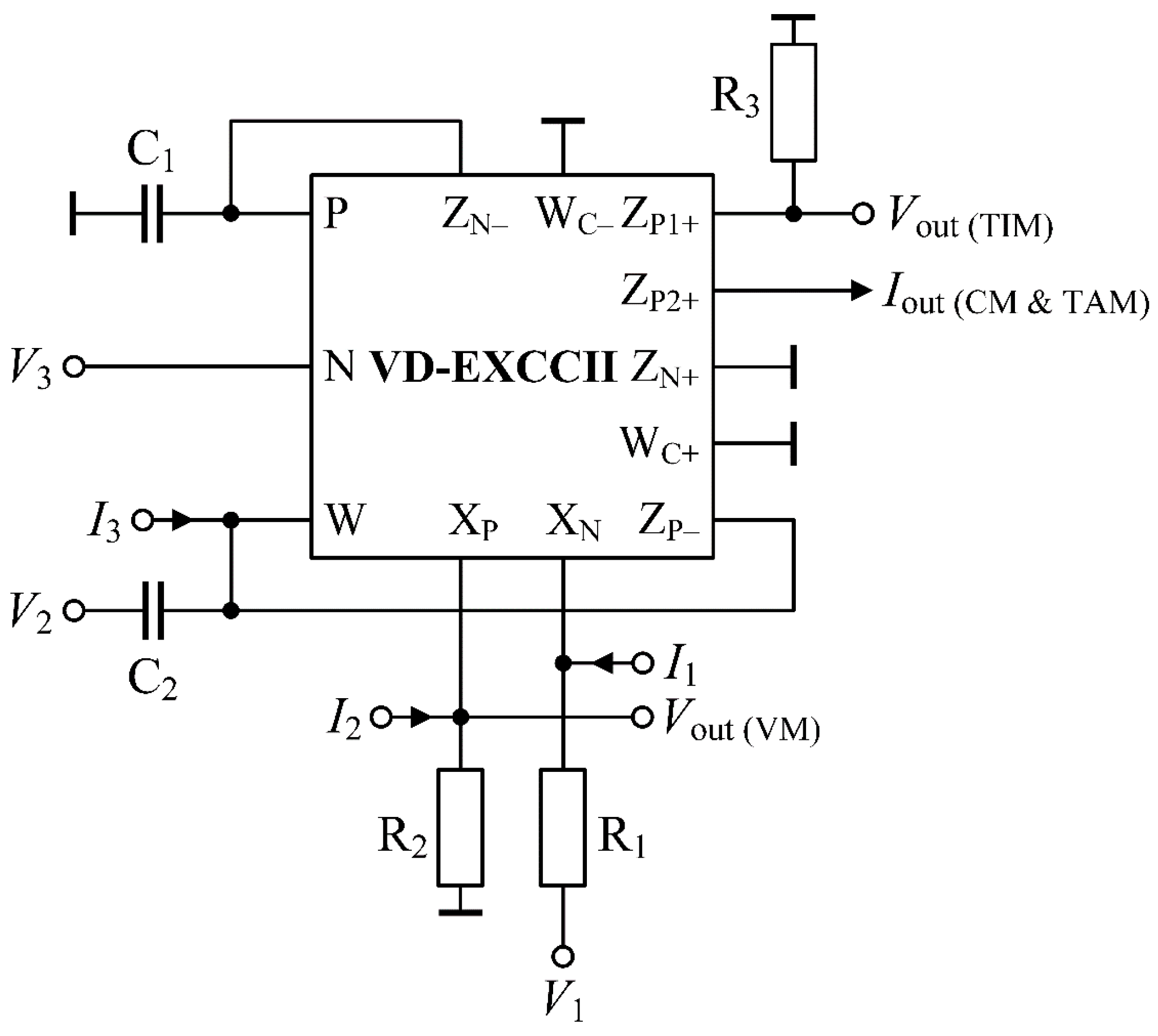
5. Simulation and Validation

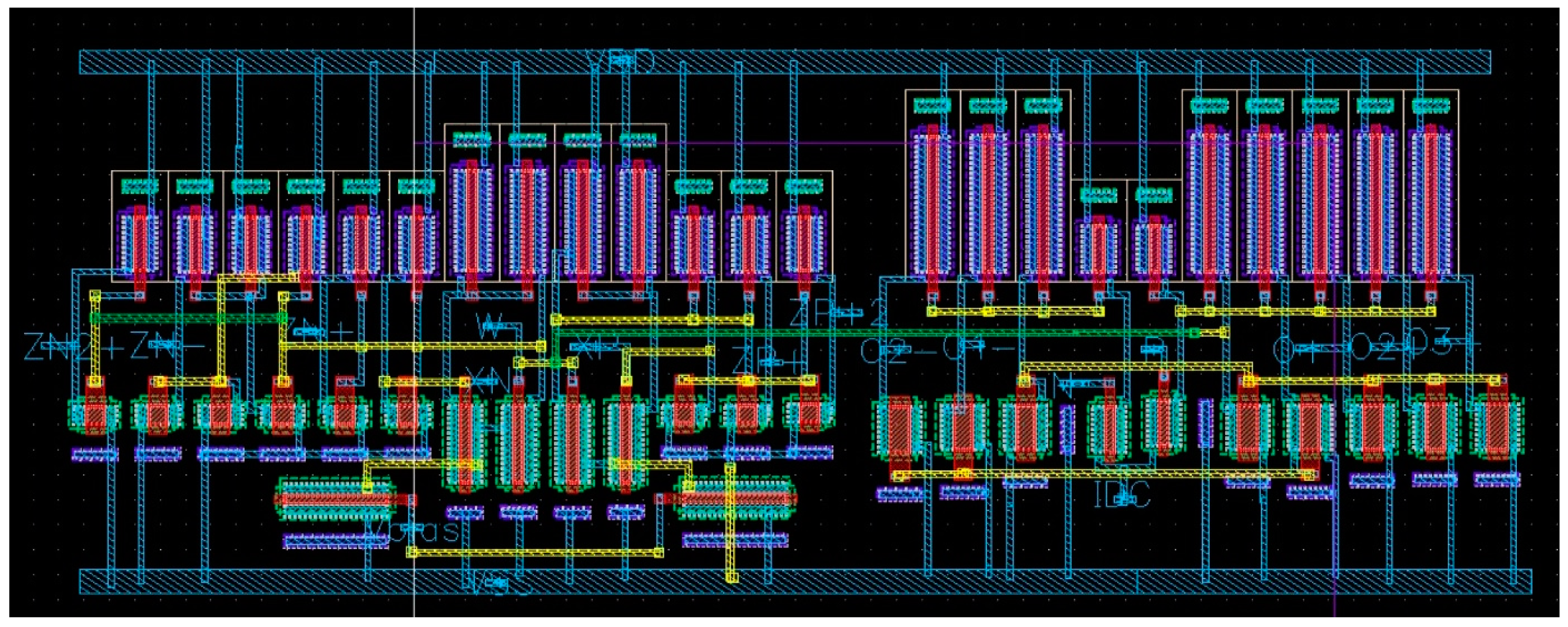
To validate the proposed mixed-mode filter, it was designed and simulated in Cadence Virtuoso design software. The VD-EXCCII was designed in 0.18 µm Silterra Malaysia technology at a supply voltage of ±1.25 V. The width and length of the transistors used are given in Table 5. The layout of the VD-EXCCII as presented in Figure 6 was drawn using the nhp and php high-performance MOS transistors from the Silterra library, and the layout verification was done using the Calibre tool. The layout occupied a total area of 54.28 × 22.80 µ m 2 . The bias current of the OTA was fixed at 120 µA resulting in transconductance of 1.0321 mS. The important design parameters were extracted from post-layout simulations and are summarized in Table 6.
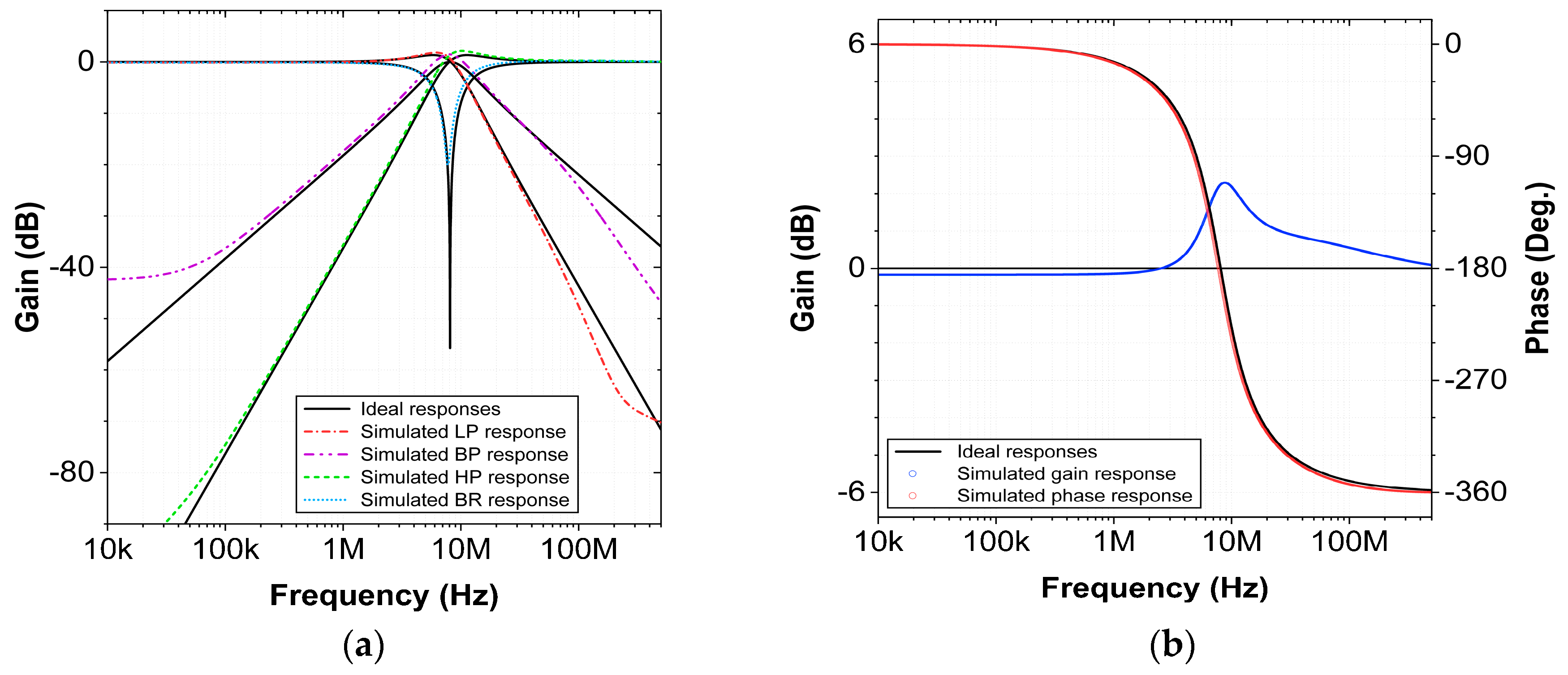
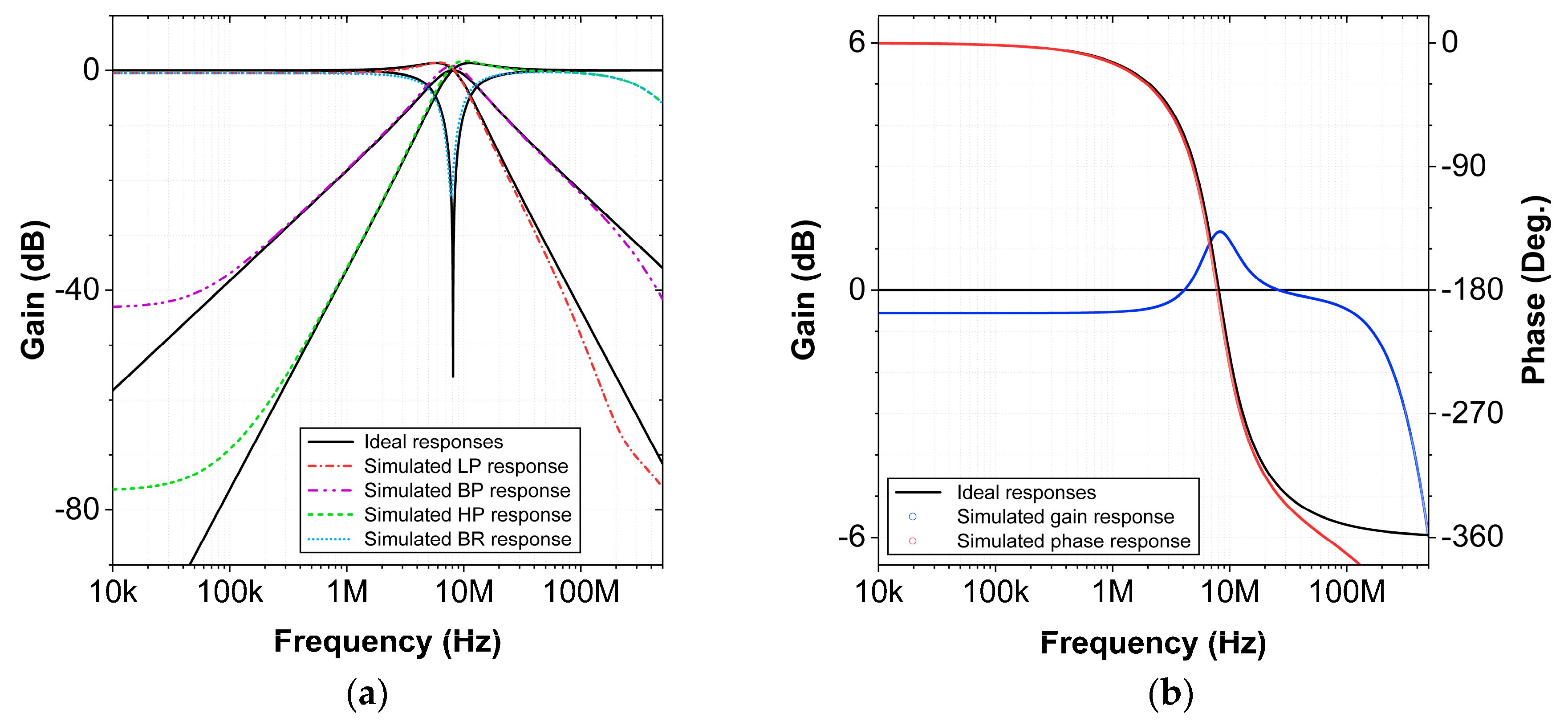
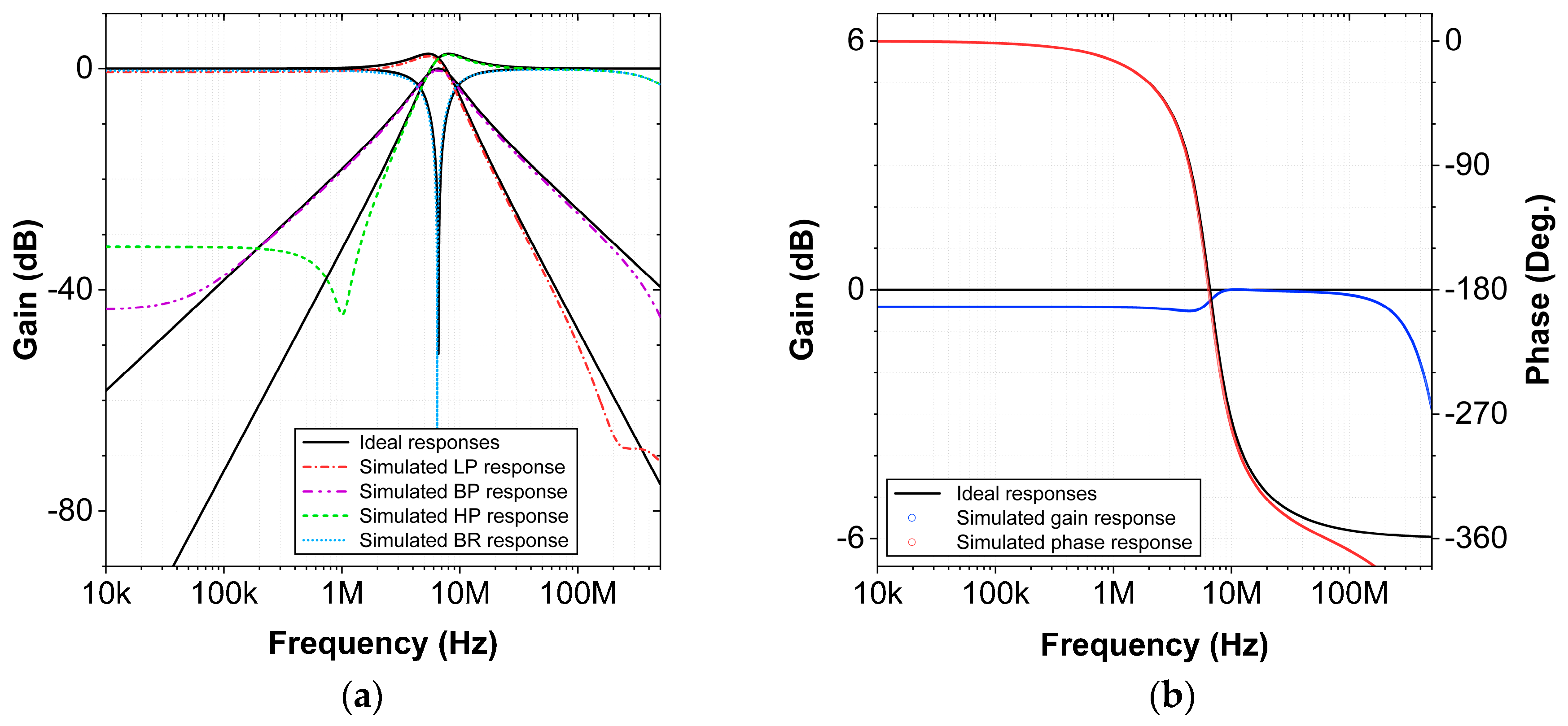
The proposed filter was tested by designing for a center frequency of 8.0844 MHz and quality factor of 1.015 by selecting the passive component as R 1 = R 2 = R 3 = 1   k Ω ,   C 1 = C 2 = 20   pF and g m 1   = 
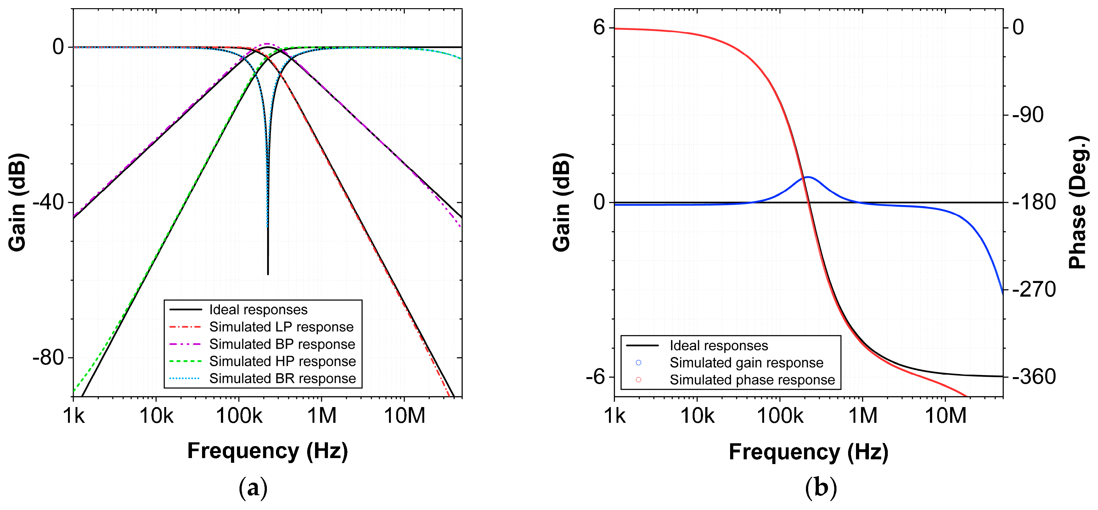
1.0321 mS. The power dissipation of the filter was found to be 5.76 mW. The five filter responses in VM, CM, TAM and TIM modes are presented in Figure 7, Figure 8, Figure 9 and Figure 10.
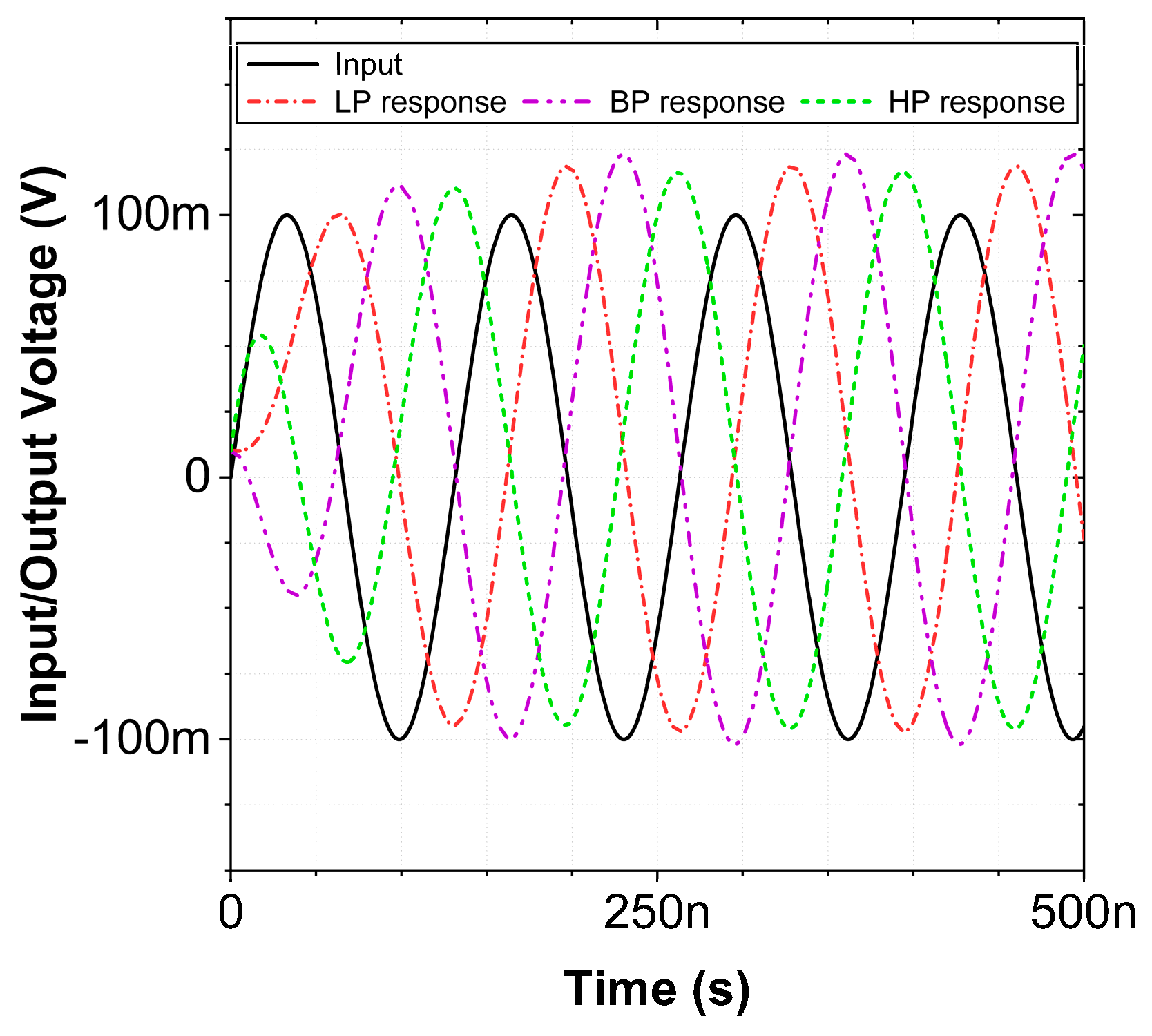
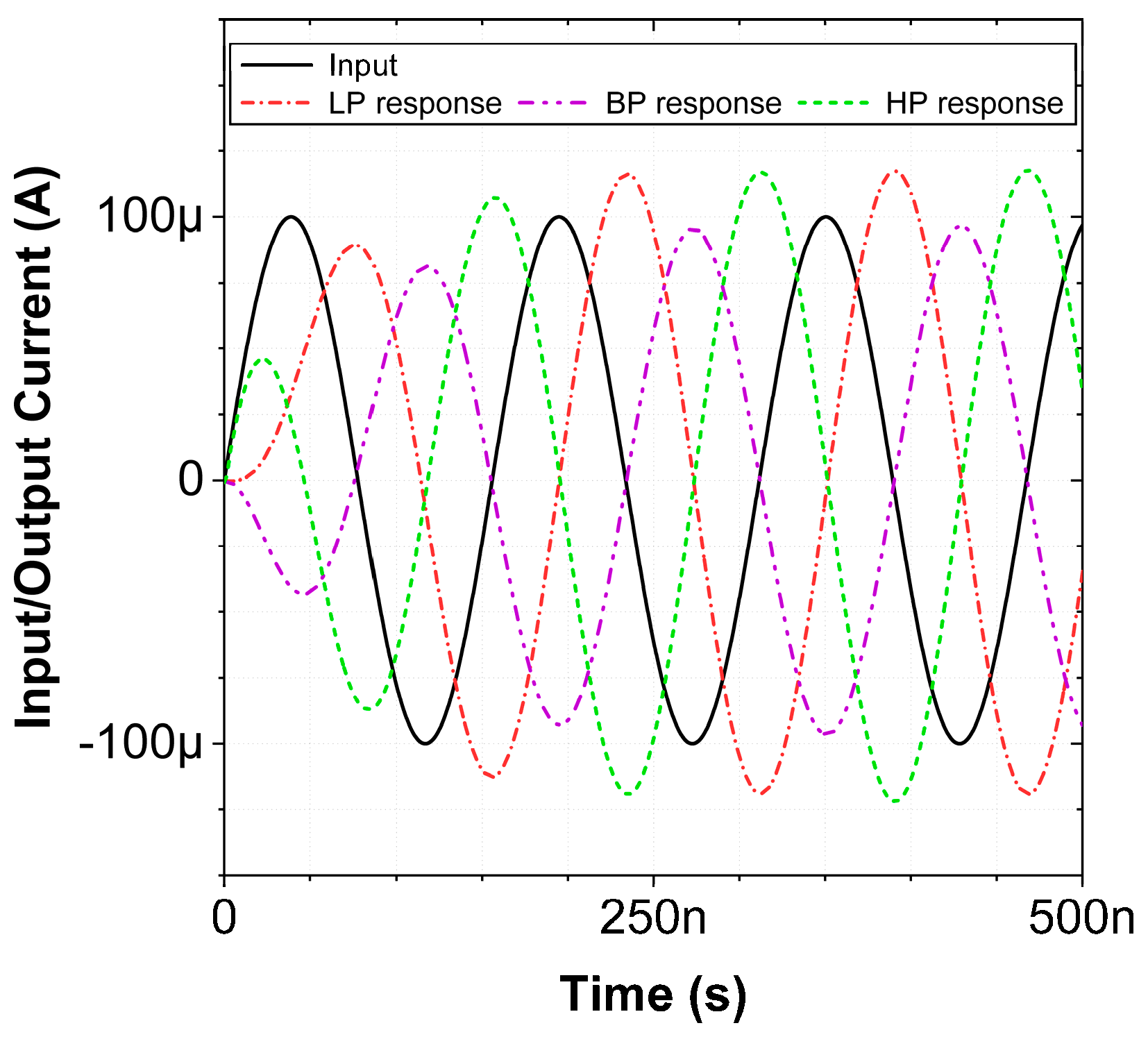
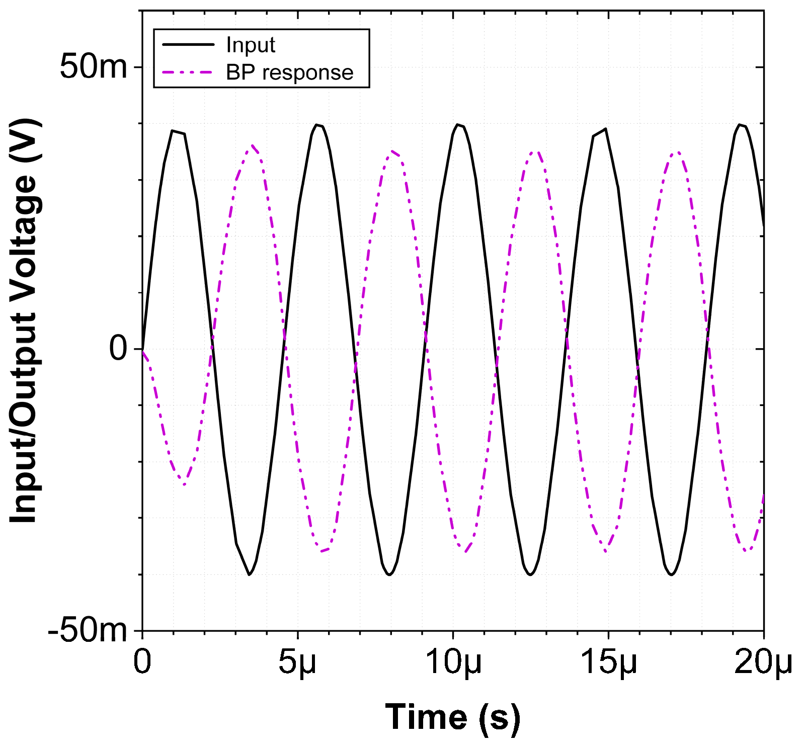
To examine the signal processing capability of the proposed universal filter, the transient analysis was carried out in VM mode for HP, LP and BP responses. A VM sinusoidal signal of 100 mVp-p and a frequency of 8.0844 MHz was applied at the input, and the output was analyzed as presented in Figure 11. It can be inferred from the figure that the phase relation between the input and LP, BP and HP outputs of the filter are correct.
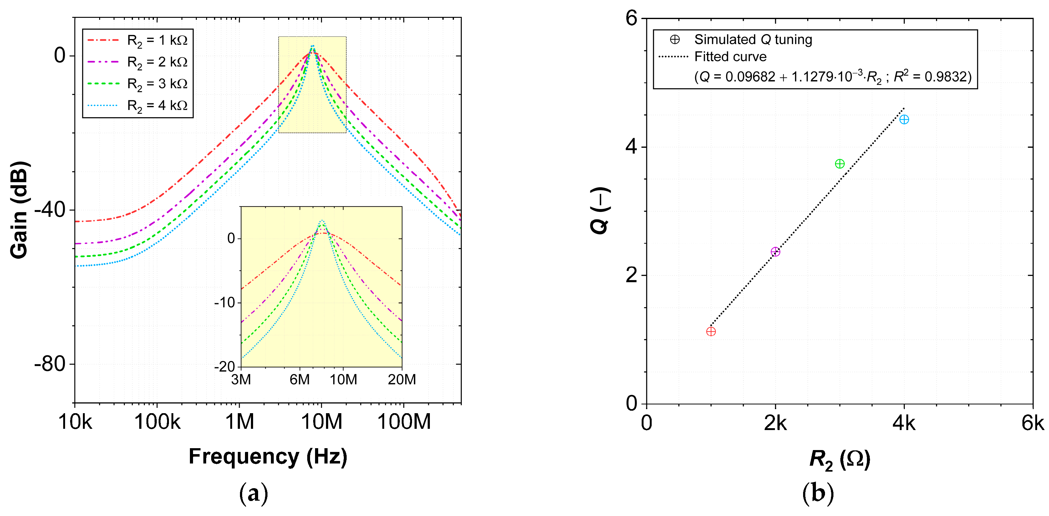
In the presented filter, the quality factor can be set independent of the pole frequency of the filter, as is clear from Equations (17) and (18). The quality factor tunability was verified by analyzing the BP response in CM for different values of R2, as shown in Figure 12. It can be deduced from Figure 12b that the quality factor of the filter can be tuned linearly. The fitting equation using a linear regression with coefficient of determination R2 = 0.9832, which indicates the fraction of the fitting values that are closest to the line of reference data, is given in 
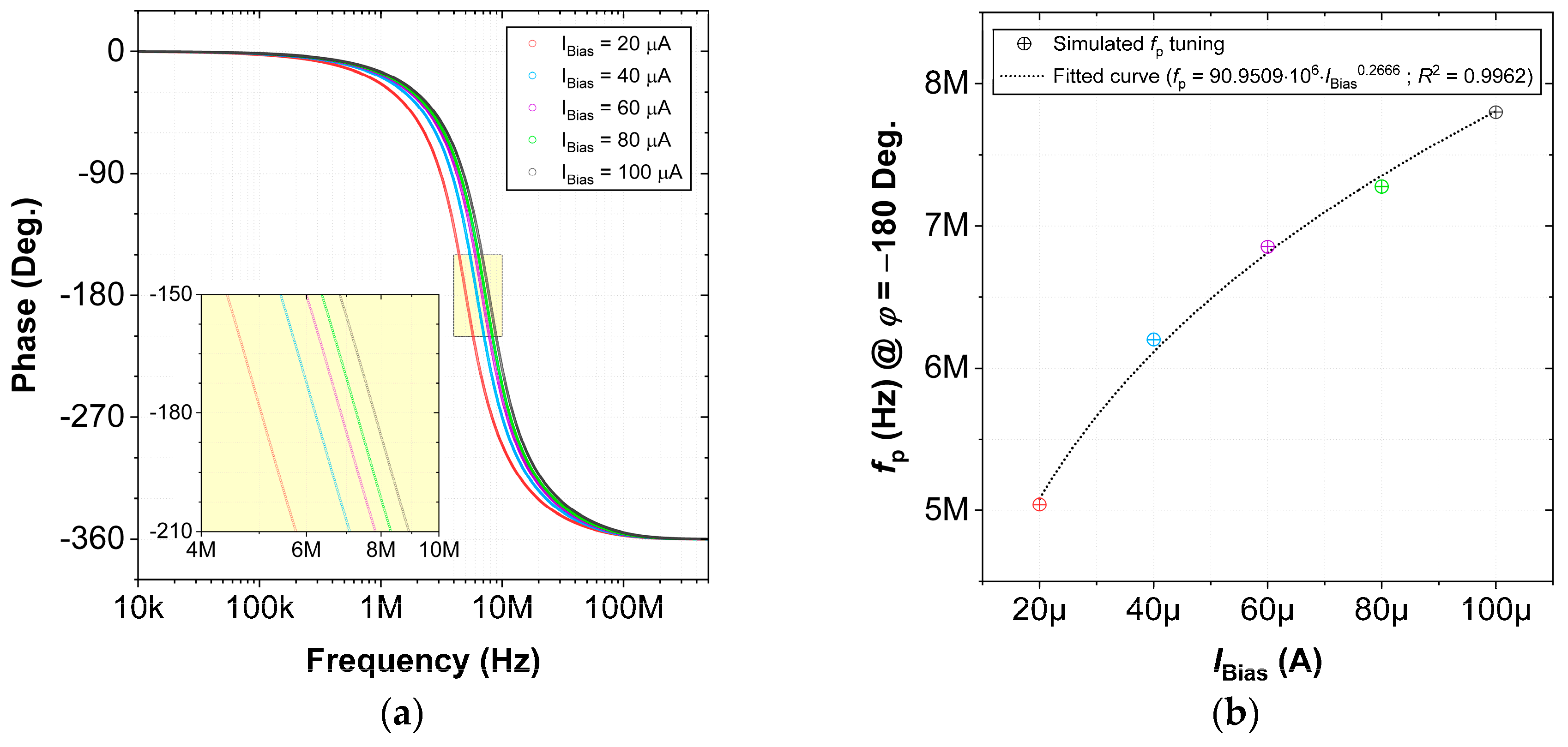
Figure 12. The pole frequency of the proposed filter can be tuned by varying the bias current of the OTA, as can be inferred from Equation (17). The tuning property is validated by plotting the VM-AP response for the different values of the OTA bias current, as shown in Figure 13. The fitting equation using a power regression with R2 = 0.9962 is given in Figure 13b.
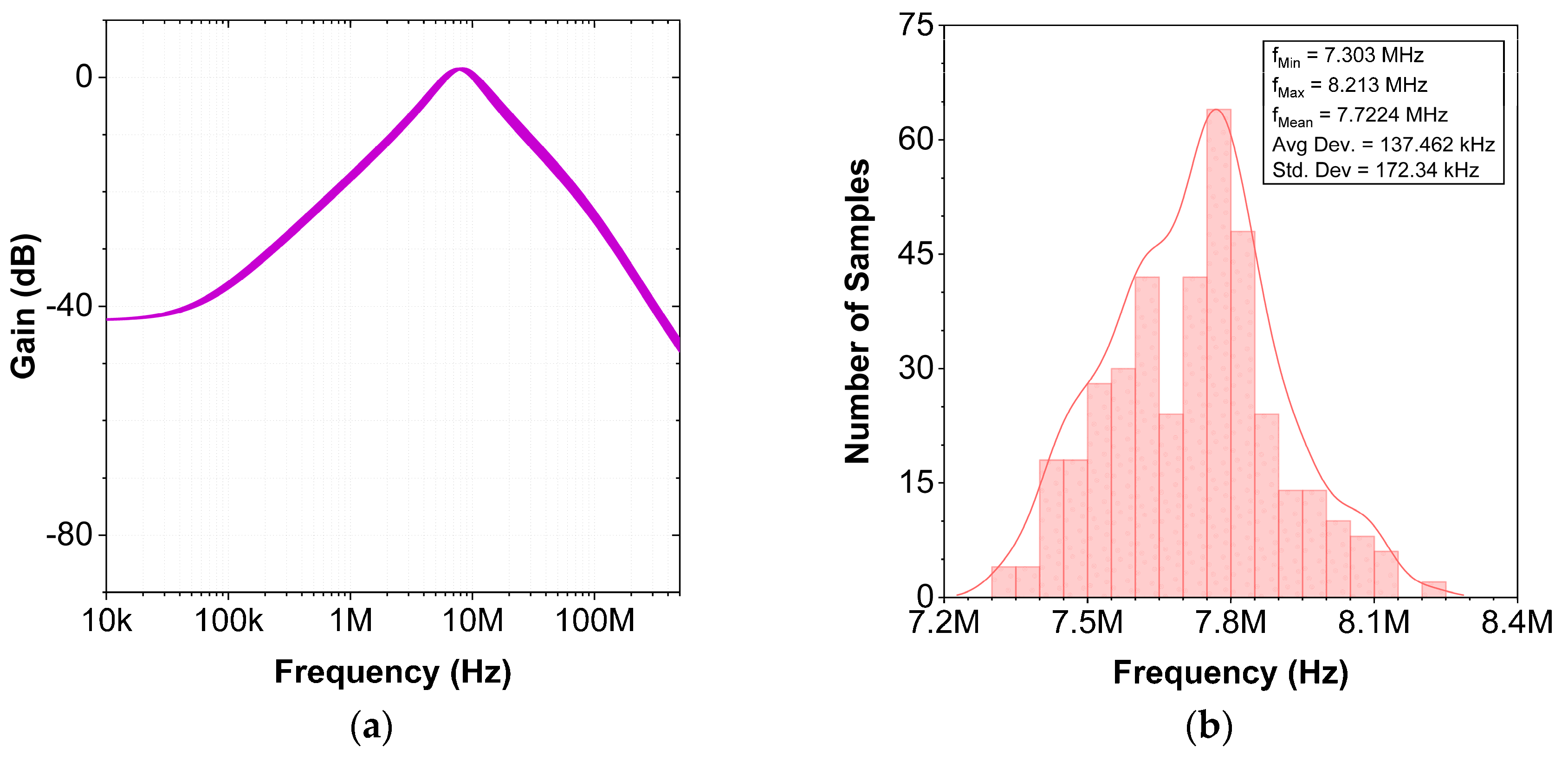
To study the effect of process spread and the non-idealities of the capacitors employed on the performance of the designed filter, a Monte Carlo analysis is carried out for 200 runs. The Monte Carlo analysis results for the VM BP response are given in Figure 14. The results for CM AP configuration are given Figure 15. Corresponding histograms demonstrate the variations of the pole frequency at −180°. The results indicate that the frequency deviation of the filter is within acceptable limits. This further validates the robustness of the design.
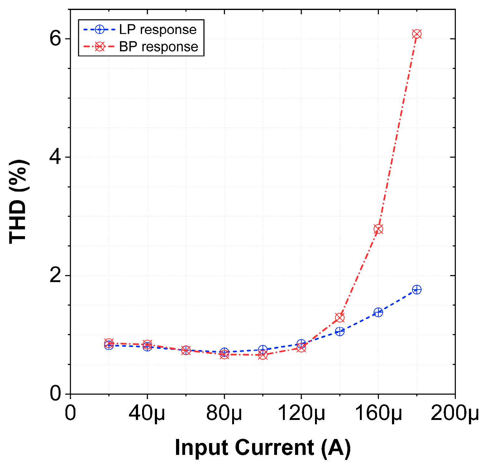
The total harmonic distortion (THD) of the filter for LP and BP responses is plotted for different input signal amplitudes for VM as shown in Figure 16. The THD plot for CM-BP/LP is presented in Figure 17. The THD remains within acceptable limits (≤7.5%) for appreciable input range.
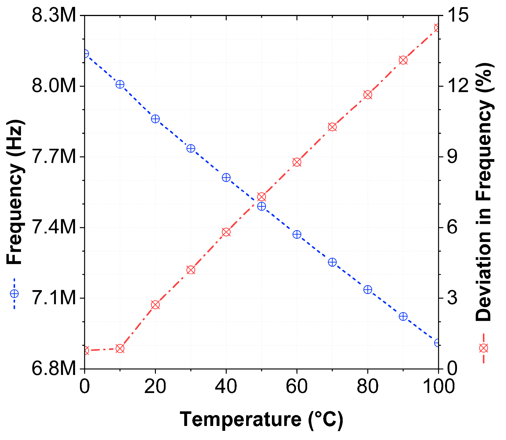
The decrease in pole frequency of the filter due to rise in temperature can be attributed to the decrease in OTA transconductance. The main factors that influence the transconductance are the threshold voltage ( V t ) and carrier mobility. V t can be approximated as a linear function of temperature [45,46] given by Equation (38):
V t ( T ) = V t ( T O ) + α V t ( T T O )
here, α V t denotes the threshold voltage temperature coefficient which, varies from −1 mV/°C to −4 mV/°C and T O is the reference temperature (300 K).
The dependence of carrier mobility on temperature is modelled by [46]:
µ N ( T ) = µ N ( T O ) ( T T O ) α µ
where α µ is the mobility temperature exponent considered as a constant approximately equal to 1.5. The Equations (38) and (39), show that the threshold voltage ( V t ) and mobility ( µ N ) exhibit a negative temperature dependence which explains the decrease in frequency with temperature, as shown in Figure 18 for CM AP response.
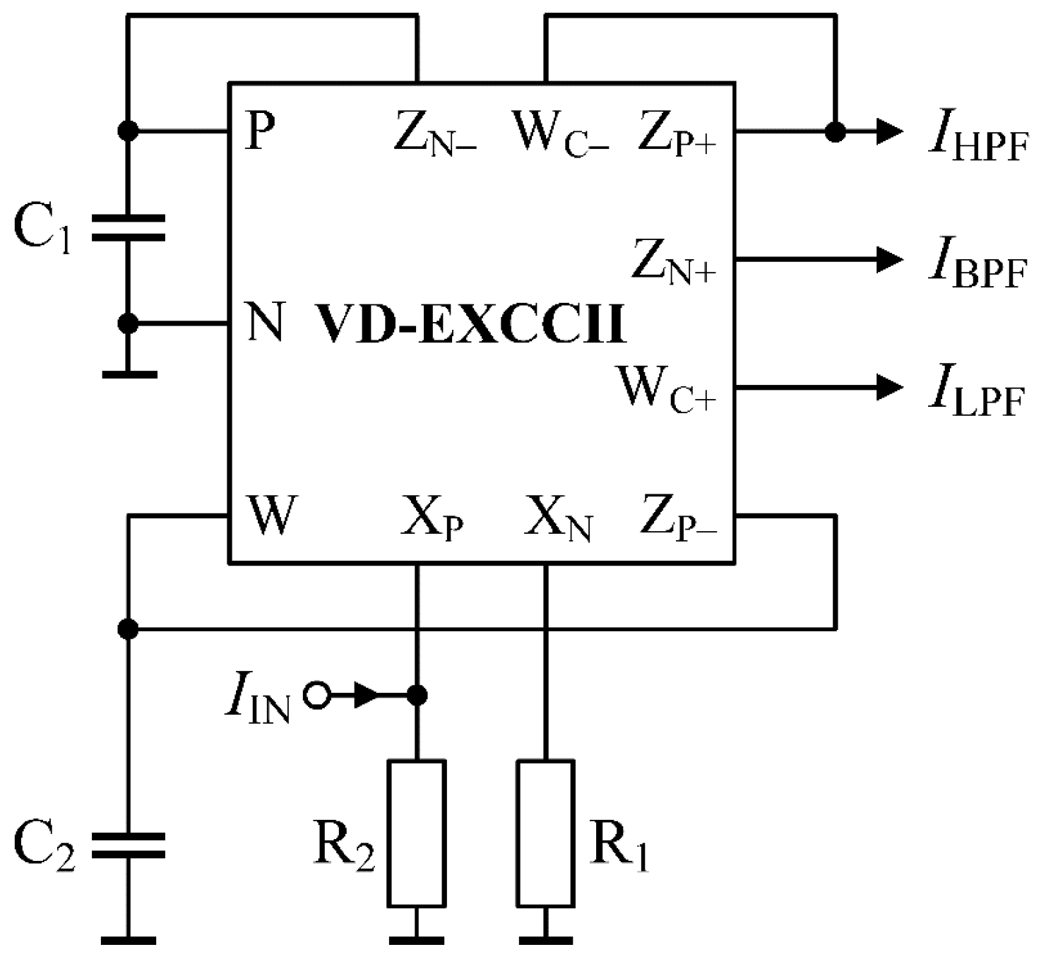
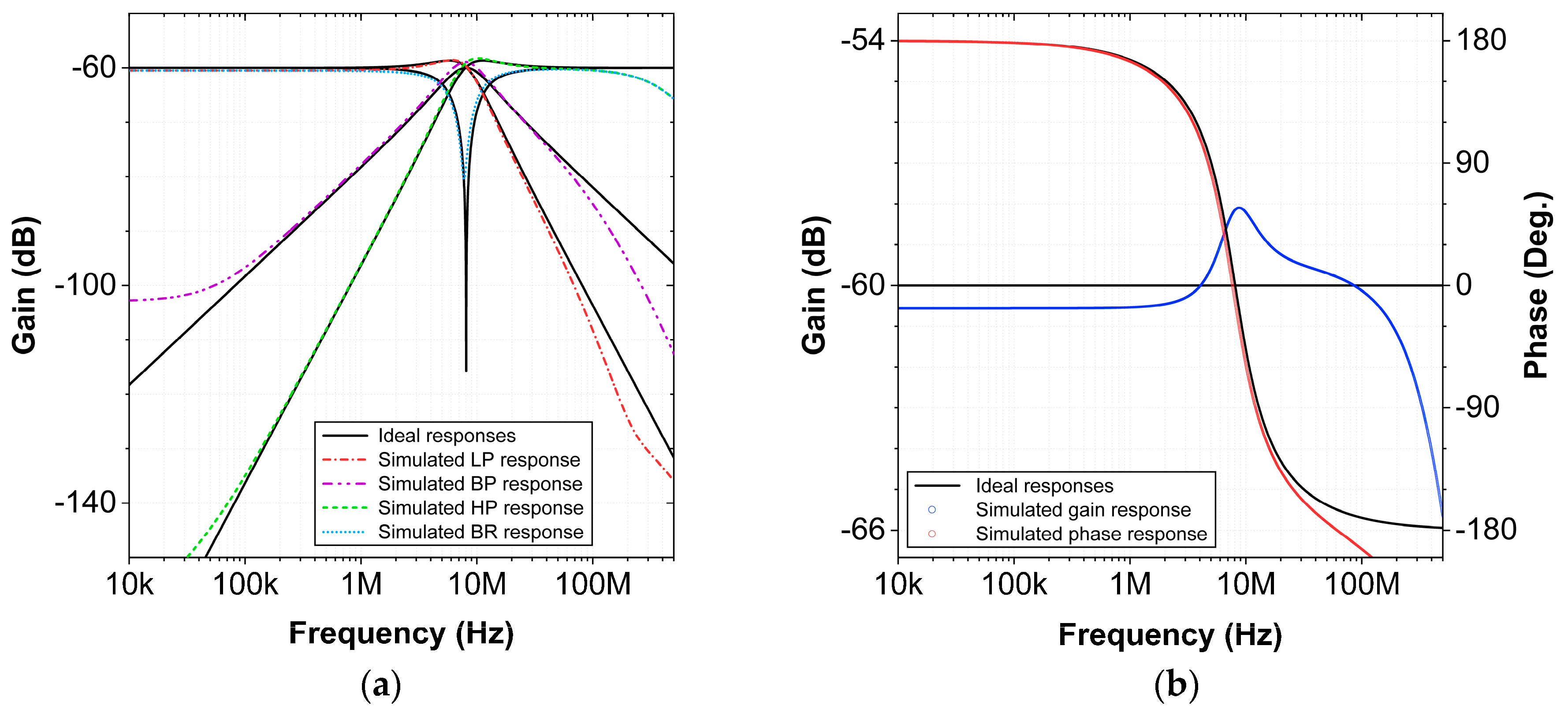
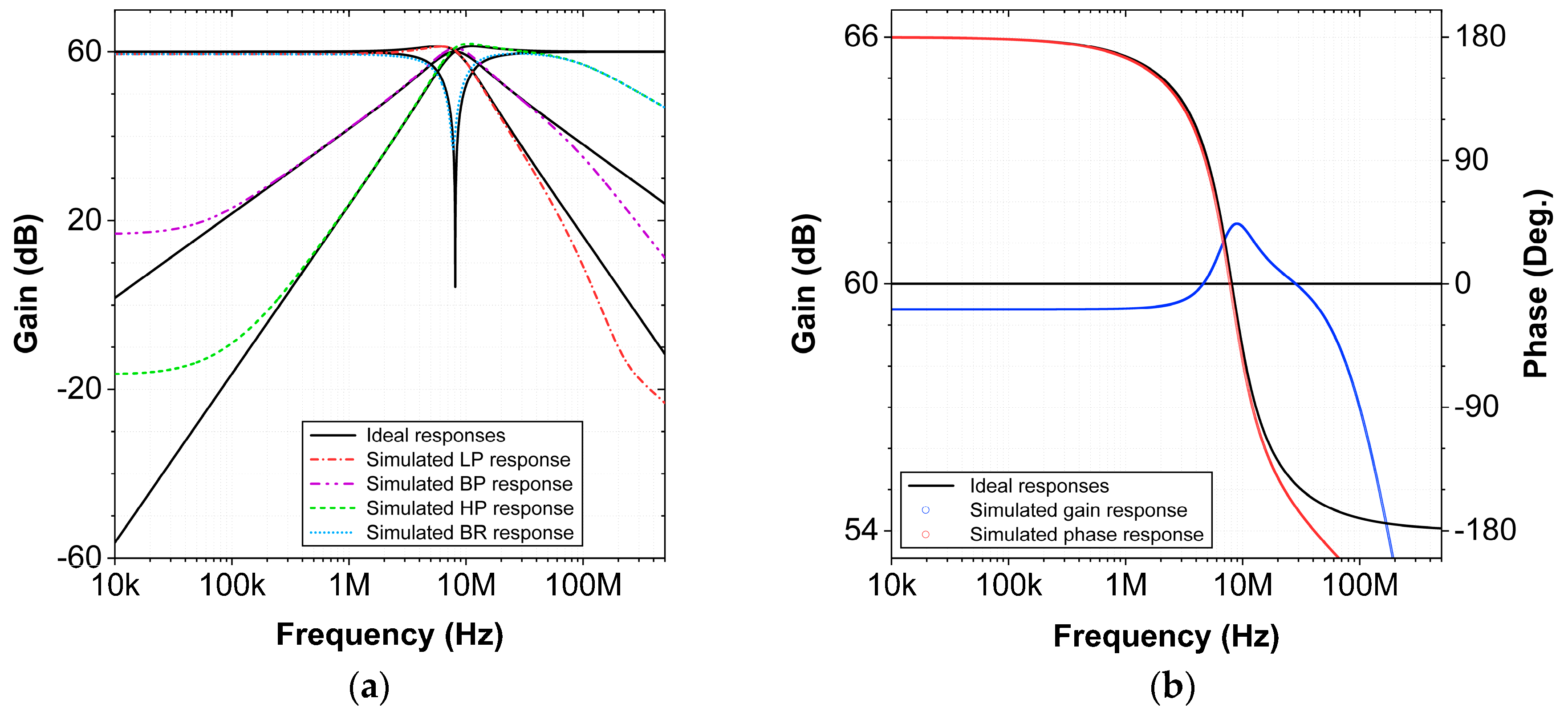
To validate the proposed CM-SIMO filter, it is designed for a center frequency of 6.4 MHz and quality factor of 1.015 by selecting passive component as R 1 = R 2 = 2   k Ω ,   C 1 = C 2 = 20   pF and gm1 = 1.0321 mS. The five filter responses in CM mode are presented in Figure 19.
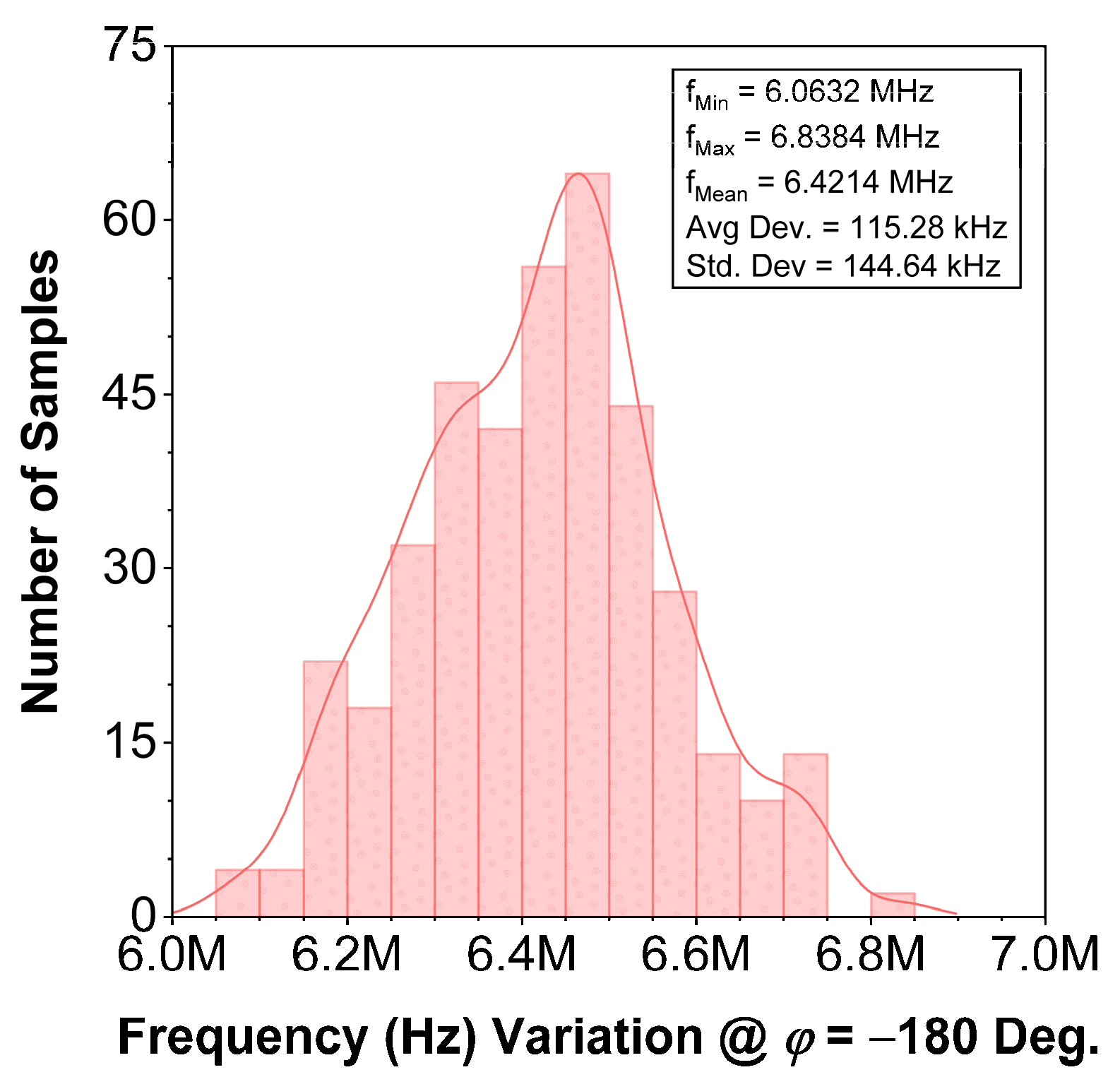
The time domain and Monte Carlo analysis results of the filter are presented in Figure 20 and Figure 21, which verify the correct filter operation. The histogram depicted in Figure 21 demonstrates the variations of the pole frequency at −180°.
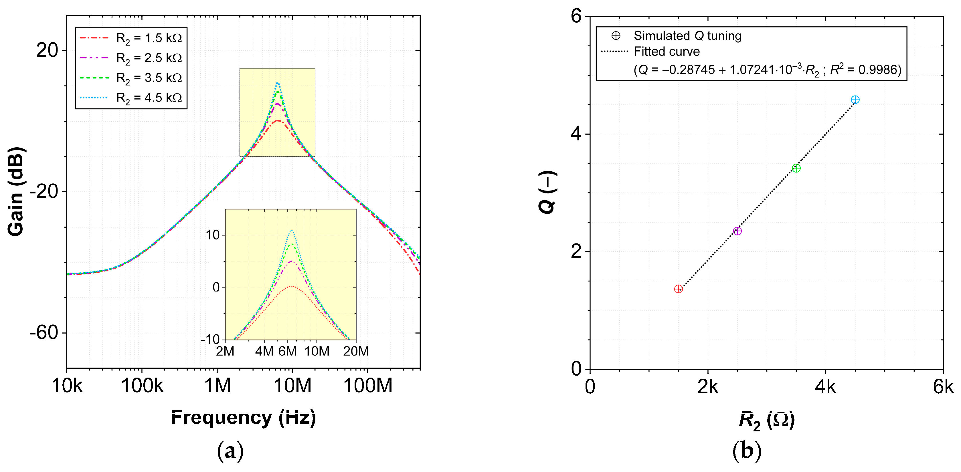
The Q factor tunability is tested for different values of resistor R 2 , as presented in Figure 22. The fitting equation using a linear regression with R2 = 0.9986 is given in Figure 22b. Furthermore, the total harmonic distortion for different input current amplitudes is shown in 
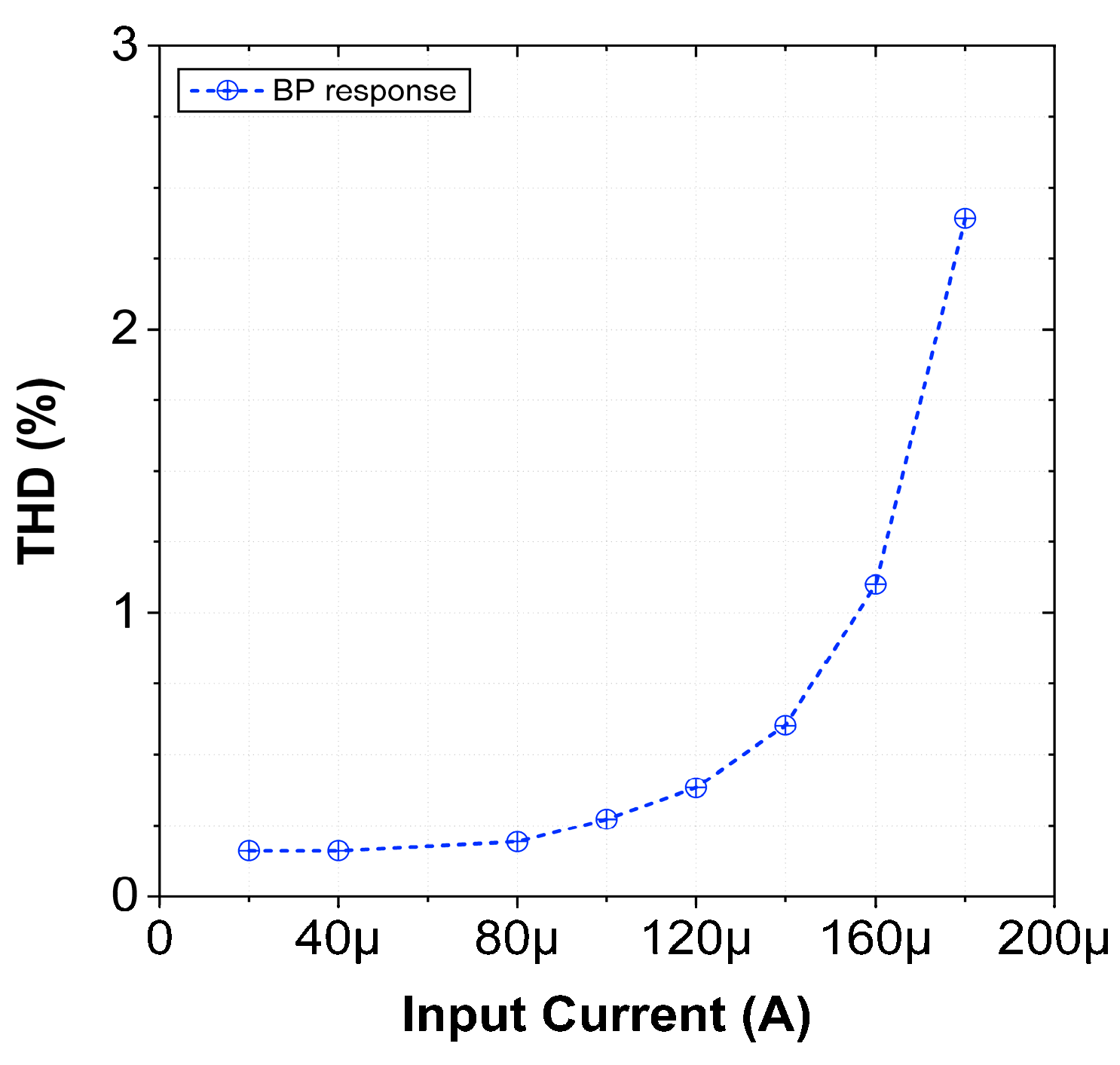
Figure 23. It can be inferred that the THD remains approximately 2.5% for a considerable signal range.
It can be concluded from the results that the characteristics of the AP filters have a slight imperfection, as all magnitude responses have a hump at the resonant frequency. This is caused by the frequency-dependent non-ideal current and voltage transfer gains and the parasitic resistances associated with the different nodes. All the mentioned non-idealities are discussed in detail in Section 4. It is also found that the linear range (dynamic range) of the circuit is mostly affected by small supply variations; however, the filter performance is not adversely affected.
To further bring out the merits of the proposed filter, a comparative analysis of the single ABBs-based mixed mode filters is carried out. It can be inferred from Table 7 that except [40], no other filter can provide all five filter responses in all four modes of operation. The latest presented filter in [47] is not a truly mixed mode and also suffers from use of negative and double input signals for filter response realization. The designs in [14,27,40,48] suffer from passive component matching requirements. The design in [48] requires a change in circuit configuration for realizing different responses, which is impractical. Although the proposed filter consumes more power compared with a few other designs, the power consumption of the filter can be reduced by redesigning the VD-EXCCII at low supply voltage and reduced bias currents.

6. Filter Realization Using Macro Models of Commercially Available Integrated Circuits AD844 and LM13700

The proposed VD-EXCCII can be easily realized by commercially available ICs, the current feedback amplifier (AD844) and OTA (LM13700). The VD-EXCCII and the proposed filter circuit are realized using the PSpice macro model of the ICs to further test the feasibility of the proposed filter circuit. The setup for realizing the VD-EXCCII and the VM filter circuit depicted in Figure 3 is presented in Figure 24.
The OTA transconductance is fixed at 2 mS by selecting +VC = 10 V and R Bias = 178.6   k Ω . The capacitors are selected equal to 1 nF and the resistors values are fixed as R 1 = 1   k Ω   and   R 2 = 500   Ω , resulting in f 0 = 225   kHz   and   Q = 0.707 . The AC analysis results of the filter are presented in Figure 25. The measured frequency is found to be 220.4 kHz, which translates into 2% error. A time domain analysis is also carried out for the VM-BP configuration. A sinusoidal signal of 40 mVp-p at the 225 kHz frequency is applied at the input of the filter and the corresponding BP output is analyzed as shown in Figure 26, which establishes the correct functioning of the filter.

7. Conclusions

This paper presents a new single VD-EXCCII-based electronically tunable mixed-mode filter structure. The filter employs only one VD-EXCCII, three resistors and two capacitors. The mixed mode filter enjoys inbuilt tunability and can realize all five filter responses in all four modes of operation (VM, CM, TAM and TIM). A CM SIMO filter can also be derived from the presented minimum component mixed mode MISO filter topology. The detailed theoretical analysis, non-ideal gain analysis and parasitic study are given. The VD-EXCCII is designed in Cadence Virtuoso software and extensive post-layout simulations are carried out to examine and validate the proposed filter in all four modes of operation. The proposed filter has all the advantages mentioned in Section 3. The filter is designed for a frequency of 8.0844 MHz with a ±1.25 V supply. The Monte Carlo analysis shows that the frequency deviation is within acceptable limits. Furthermore, the THD is within 5% for a considerable voltage/current input signal range. The power dissipation of the filter is found to be 5.76 mW. The VD-EXCCII and the mixed mode filter are also designed and tested using the models of commercially available ICs the AD844 and LM13700 in PSpice. The simulation results are found consistent with the theoretical predictions.

Author Contributions

Conceptualization, M.F., M.A.A. and J.S.; methodology, M.F., N.H., M.A.A. and J.S.; software, M.F.; validation, M.F. and M.A.A.; formal analysis, M.F., N.H. and J.S.; investigation, M.F., N.H. and J.S.; resources, M.A.A. and J.S.; data curation, M.F., N.H. and M.A.A.; writing—original draft preparation, M.F., N.H, M.A.A. and J.S.; writing—review and editing, M.F., N.H. and J.S.; visualization, N.H.; supervision, J.S.; project administration, M.F. and M.A.A.; funding acquisition, N.H., M.A.A. and J.S. All authors have read and agreed to the published version of the manuscript.

Funding

Part of this work was carried out at the Institute of Microengineering and Nanoelectronics (IMEN), University Kebangsaan Malaysia (UKM). This work is funded by the Ministry of Education Malaysia under grant (FRGS/1/2018/TK04/UKM/02/1) and AKU254:HICoE (Fasa II) ‘MEMS for Biomedical Devices (artificial kidney)’.

Acknowledgments

We would like to thank the anonymous reviewers for their insightful comments and suggestions.

Conflicts of Interest

The authors declare no conflict of interest. The funders had no role in the design of the study; in the collection, analyses or interpretation of data; in the writing of the manuscript, or in the decision to publish the results.

Abbreviations

The following abbreviations are used in this manuscript:
α P / N ,   α P / N Frequency dependent non-ideal current gains
α V t Threshold voltage temperature coefficient
β P / N Frequency dependent non-ideal voltage gains
ε g m , ε g m Transconductance errors
ε i P , ε i N Current tracking errors
ε v ( P , N ) Voltage tracking errors
γ ,   γ Frequency dependent non-ideal transconductance transfer gains
µCarrier mobility
ABBActive building blocks
APAll pass
BPBand pass
BRBand reject
CoxGate oxide capacitance per unit area
CCIISecond-generation current conveyor
CFOACurrent feedback operational amplifier
CMCurrent-mode
DDCCDifferential difference current conveyor
DPCCIIDigitally programmable second-generation current conveyor
DVCCDifferential voltage current conveyor
HPHigh pass
ICCIIInverting second-generation current conveyor
LEffective length of the channel
LPLow pass
MISOMulti input single output
MOCCCIIMulti output current controlled current conveyor
MOCCIIMulti output second-generation current conveyor
OTAOperational transconductance amplifier
QQuality factor
SIMOSingle input multi output
TIMTrans-impedance-mode
VtThreshold voltage
VDBAVoltage differencing buffered amplifier
VDCCVoltage differencing current conveyor
VD-EXCCIIVoltage Differencing Extra X Current Conveyor
VDTAVoltage differencing transconductance amplifier
VMVoltage-mode
WEffective channel width

References

  1. Mohan, P.A. Current-Mode VLSI Analog Filters: Design and Applications; Springer Science & Business Media: Berlin/Heidelberg, Germany, 2012. [Google Scholar]
  2. Ferri, G.; Guerrini, N.C. Low-Voltage Low-Power CMOS Current Conveyors; Springer Science & Business Media: Berlin/Heidelberg, Germany, 2003. [Google Scholar]
  3. Senani, R.; Bhaskar, D.; Singh, A. Current Conveyors: Variants, Applications and Hardware Implementations; Springer: Berlin/Heidelberg, Germany, 2014. [Google Scholar]
  4. Mohammad, F.; Sampe, J.; Shireen, S.; Ali, S.H.M. Minimum passive components based lossy and lossless inductor simulators employing a new active block. AEU Int. J. Electron. Commun. 2017, 82, 226–240. [Google Scholar] [CrossRef]
  5. Raut, R.; Swamy, M.N. Modern Analog Filter Analysis and Design: A Practical Approach; John Wiley & Sons: Hoboken, NJ, USA, 2010. [Google Scholar]
  6. Abuelma’Atti, M.T.; Bentrcia, A. A Novel mixed-mode CCII-based filter. Act. Passiv. Electron. Compon. 2004, 27, 197–205. [Google Scholar] [CrossRef] [Green Version]
  7. Abuelma’Atti, M.T.; Bentrcia, A.; Al-Shahrani, S.M. A novel mixed-mode current-conveyor-based filter. Int. J. Electron. 2004, 91, 191–197. [Google Scholar] [CrossRef]
  8. Abuelma’Atti, M.T. A Novel mixed-mode current-controlled current-conveyor-based filter. Act. Passiv. Electron. Compon. 2003, 26, 185–191. [Google Scholar] [CrossRef] [Green Version]
  9. Abuelma’Atti, M.T.; Bentrcia, A. A Novel mixed-mode OTA-C filter. Frequenz 2003, 57, 157–159. [Google Scholar] [CrossRef]
  10. Singh, V.K.; Singh, A.K.; Bhaskar, D.R.; Senani, R. Novel mixed-mode universal biquad configuration. IEICE Electron. Express 2005, 2, 548–553. [Google Scholar] [CrossRef] [Green Version]
  11. Shah, N.A.; Malik, M.A. Multifunction mixed-mode filter using FTFNs. Analog. Integr. Circuits Signal Process. 2006, 47, 339–343. [Google Scholar] [CrossRef]
  12. Pandey, N.; Paul, S.K.; Bhattacharyya, A.; Jain, S.B. A new mixed mode biquad using reduced number of active and passive elements. IEICE Electron. Express 2006, 3, 115–121. [Google Scholar] [CrossRef] [Green Version]
  13. Ibrahim, M.A. Design and analysis of a mixed-mode universal filter using dual-output operational transconductance amplifiers (DO-OTAs). In Proceedings of the 2008 International Conference on Computer and Communication Engineering, Kuala Lumpur, Malaysia, 13–15 May 2008; pp. 915–918. [Google Scholar]
  14. Lee, C.-N.; Chang, C.-M. Single FDCCII-based mixed-mode biquad filter with eight outputs. AEU—Int. J. Electron. Commun. 2009, 63, 736–742. [Google Scholar] [CrossRef]
  15. Li, Z. Mixed-mode universal filter using MCCCII. AEU—Int. J. Electron. Commun. 2009, 63, 1072–1075. [Google Scholar] [CrossRef]
  16. Minaei, S.; Ibrahim, M.A. A mixed-mode KHN-biquad using DVCC and grounded passive elements suitable for direct cascading. Int. J. Circuit Theory Appl. 2009, 37, 793–810. [Google Scholar] [CrossRef]
  17. Chen, H.-P.; Liao, Y.-Z.; Lee, W.-T. Tunable mixed-mode OTA-C universal filter. Analog. Integr. Circuits Signal Process. 2008, 58, 135–141. [Google Scholar] [CrossRef]
  18. Maheshwari, S.; Singh, S.; Chauhan, D. Electronically tunable low-voltage mixed-mode universal biquad filter. IET Circuits Devices Syst. 2011, 5, 149. [Google Scholar] [CrossRef]
  19. Lee, C.-N.; Lee, C.-N. Multiple-mode OTA-C universal biquad filters. Circuits Syst. Signal Process. 2009, 29, 263–274. [Google Scholar] [CrossRef]
  20. Pandey, N.; Paul, S.K.; Bhattacharyya, A.; Jain, S. Realization of generalized mixed mode universal filter using CCCIIs. J. Act. Passive Electron. Devices 2010, 5, 279–293. [Google Scholar]
  21. Singh, S.; Maheshwari, S.; Chauhan, D. Electronically tunable current/voltage-mode universal biquad filter using CCCCTA. Int. J. Recent Trends in Eng. Technol. 2010, 3, 71–76. [Google Scholar]
  22. Liao, W.-B.; Gu, J.-C. SIMO type universal mixed-mode biquadratic filter. Indian J. Eng. Mater. Sci. 2011, 18, 443–448. [Google Scholar]
  23. Kumngern, M.; Junnapiya, S. Mixed-mode universal filter using OTAs. In Proceedings of the 2012 IEEE International Conference on Cyber Technology in Automation, Control, and Intelligent Systems (CYBER), Bangkok, Thailand, 27–31 May 2012; pp. 119–122. [Google Scholar]
  24. Pandey, N.; Paul, S.K. Mixed mode universal filter. J. Circuits Syst. Comput. 2013, 22, 1250064. [Google Scholar] [CrossRef]
  25. Kacar, F.; Kuntman, A.; Kuntman, H. Mixed-mode biquad filter employing single active element. In Proceedings of the 2013 IEEE 4th Latin American Symposium on Circuits and Systems (LASCAS), Cusco, Peru, 27 February–1 March 2013; pp. 1–4. [Google Scholar] [CrossRef]
  26. Yeşil, A.; Kaçar, F. Electronically tunable resistorless mixed mode biquad filters. Radioengineering 2013, 22, 1016–1025. [Google Scholar]
  27. Yuce, E. Fully integrable mixed-mode universal biquad with specific application of the CFOA. AEU—Int. J. Electron. Commun. 2010, 64, 304–309. [Google Scholar] [CrossRef]
  28. Wang, L.; Wang, C.; Zhang, J.; Liang, X.; Jiang, S. A new mixed-mode filter based on MDDCCs. In Proceedings of the Seventh International Conference on Graphic and Image Processing (ICGIP 2015), Singapore, 23–25 October 2015; Volume 981717. [Google Scholar]
  29. Lee, C.-N. Independently tunable mixed-mode universal biquad filter with versatile input/output functions. AEU Int. J. Electron. Commun. 2016, 70, 1006–1019. [Google Scholar] [CrossRef]
  30. Lee, C.-N. Mixed-Mode Universal Biquadratic Filter with No Need of Matching Conditions. J. Circuits Syst. Comput. 2016, 25, 1650106. [Google Scholar] [CrossRef]
  31. Chen, H.-P.; Yang, W.-S. Electronically Tunable Current Controlled Current Conveyor Transconductance Amplifier-Based Mixed-Mode Biquadratic Filter with Resistorless and Grounded Capacitors. Appl. Sci. 2017, 7, 244. [Google Scholar] [CrossRef] [Green Version]
  32. Chamnanphai, V. Electronically Tunable SIMO Mixed-mode universal filter using VDTAs. Przegląd Elektrotechniczny 2017, 1, 209–213. [Google Scholar] [CrossRef] [Green Version]
  33. Parvizi, M.; Taghizadeh, A.; Mahmoodian, H.; Kozehkanani, Z.D. A Low-Power Mixed-Mode SIMO Universal G m–C Filter. J. Circuits Syst. Comput. 2017, 26, 1750164. [Google Scholar] [CrossRef]
  34. Horng, J.-W.; Wu, C.-M.; Herencsar, N. Current-mode and transimpedance-mode universal biquadratic filter using two current conveyors. Indian J. Eng. Mater. Sci. 2017, 24, 461–468. [Google Scholar]
  35. Cini, U.; Aktan, M. Dual-mode OTA based biquadratic filter suitable for current-mode applications. AEU Int. J. Electron. Commun. 2017, 80, 43–47. [Google Scholar] [CrossRef]
  36. Chaturvedi, B.; Mohan, J.; Kumar, A. A New Versatile Universal Biquad Configuration for Emerging Signal Processing Applications. J. Circuits Syst. Comput. 2018, 27, 1850196. [Google Scholar] [CrossRef]
  37. Tsukutani, T.; Yabuki, N. A DVCC-Based Mixed-Mode Biquadratic Circuit. J. Electr. Eng. 2018, 6, 52–56. [Google Scholar] [CrossRef] [Green Version]
  38. Bhaskar, D.R.; Raj, A.; Kumar, P. Mixed-mode universal biquad filter using OTAs. J. Circuits Syst. Comput. 2019, 29, 2050162. [Google Scholar] [CrossRef]
  39. Lee, C.-N.; Yang, W.-C. General Mixed-Mode Single-Output DDCC-based Universal Biquad Filter. Int. J. Eng. Res. 2020, 9, 744–749. [Google Scholar] [CrossRef]
  40. Singh, S.V.; Tomar, R.S.; Chauhan, D.S. A new electronically tunable universal mixed-mode biquad filter. J. Eng. Res. 2016, 4, 1–21. [Google Scholar] [CrossRef]
  41. Ettaghzouti, T.; Hassen, N.; Besbes, K. A Novel multi-input single-output mixed-mode universal filter employing second generation current conveyor circuit. In Sensors, Circuits & Instrumentation Systems: Extended Papers 2017; De Gruyter Oldenbourg: Berlin, Germany, 2018; Volume 6, pp. 53–64. [Google Scholar]
  42. Maheshwari, S. Realization of Simple Electronic Functions Using EXCCII. J. Circuits Syst. Comput. 2017, 26, 1750171. [Google Scholar] [CrossRef]
  43. Baker, R.J. CMOS: Circuit Design, Layout, and Simulation; John Wiley & Sons: Hoboken, NJ, USA, 2019. [Google Scholar]
  44. Han, I.; Park, S. Voltage-controlled linear resistor by two MOS transistors and its application to active RC filter MOS integration. Proc. IEEE 1984, 72, 1655–1657. [Google Scholar] [CrossRef]
  45. Tsividis, Y.; McAndrew, C. Operation and Modeling of the MOS Transistor; Oxford University Press: Oxford, UK, 2011. [Google Scholar]
  46. Filanovsky, I.; Allam, A. Mutual compensation of mobility and threshold voltage temperature effects with applications in CMOS circuits. IEEE Trans. Circuits Syst. I Fundam. Theory Appl. 2001, 48, 876–884. [Google Scholar] [CrossRef]
  47. Agrawal, D.; Maheshwari, S. High-Performance Electronically Tunable Analog Filter Using a Single EX-CCCII. Circuits Syst. Signal. Process. 2020, 1–25. [Google Scholar] [CrossRef]
  48. Koksal, M.; Oner, S.E.; Sagbas, M. A new second-order multi-mode multi-funtion filter using a single CDBA. In Proceedings of the 2009 European Conference on Circuit Theory and Design, Antalya, Turkey, 23–27 August 2009; pp. 699–702. [Google Scholar]
Figure 1. Block diagram of VD-EXCCII.
Applsci 11 00055 g001
Figure 2. CMOS implementation of VD-EXCCII.
Applsci 11 00055 g002
Figure 3. Proposed mixed mode universal filter employing VD-EXCCII.
Applsci 11 00055 g003
Figure 4. Proposed CM SIMO filter.
Applsci 11 00055 g004
Figure 5. Non-ideal model of VD-EXCCII with parasitics.
Applsci 11 00055 g005
Figure 6. Layout of the VD-EXCCII.
Applsci 11 00055 g006
Figure 7. VM MISO configuration: (a) frequency responses of the LP, BP, HP and BR filter and (b) gain and phase responses of the AP filter.
Applsci 11 00055 g007
Figure 8. TAM MISO configuration: (a) frequency responses of the LP, BP, HP and BR filter and (b) gain and phase responses of the AP filter.
Applsci 11 00055 g008
Figure 9. CM MISO configuration: (a) frequency responses of the LP, BP, HP, and BR filter and (b) gain and phase responses of the AP filter.
Applsci 11 00055 g009
Figure 10. TIM MISO configuration: (a) frequency responses of the LP, BP, HP and BR filter and (b) gain and phase responses of the AP filter.
Applsci 11 00055 g010
Figure 11. VM MISO configuration: transient analysis results for LP, BP and HP filter configurations.
Applsci 11 00055 g011
Figure 12. CM MISO configuration: (a) frequency responses and (b) quality factor tuning for different resistor values in BP filter.
Applsci 11 00055 g012
Figure 13. VM MISO configuration: (a) phase responses and (b) pole frequency tuning for different OTA bias current values for AP response.
Applsci 11 00055 g013
Figure 14. VM MISO configuration: (a) the Monte Carlo analysis results for BP response and (b) the corresponding histogram.
Applsci 11 00055 g014
Figure 15. CM MISO configuration: (a) the Monte Carlo analysis results and (b) the corresponding histogram.
Applsci 11 00055 g015
Figure 16. Total harmonic distortion of VM-BP and VM-LP.
Applsci 11 00055 g016
Figure 17. Total harmonic distortion of CM-BP.
Applsci 11 00055 g017
Figure 18. CM MISO configuration: variation of filter pole frequency with temperature and percentage of deviation from the designed frequency for AP response.
Applsci 11 00055 g018
Figure 19. CM SIMO configuration: (a) frequency responses of the LP, BP, HP and BR filter and (b) gain and phase responses of the AP filter.
Applsci 11 00055 g019
Figure 20. CM SIMO configuration: transient analysis results for LP, HP and BP filter configurations.
Applsci 11 00055 g020
Figure 21. CM SIMO configuration: the Monte Carlo analysis results for AP configuration.
Applsci 11 00055 g021
Figure 22. CM SIMO configuration: (a) frequency responses and (b) quality factor tuning for different resistor values in BP filter.
Applsci 11 00055 g022
Figure 23. CM SIMO configuration: total harmonic distortion of CM-BP.
Applsci 11 00055 g023
Figure 24. Scheme for the implementation of the VM filter depicted in Figure 3 using commercially available ICs.
Applsci 11 00055 g024
Figure 25. VM responses of the filter: (a) frequency responses of the LP, BP, HP and BR filter and (b) gain and phase responses of the AP filter.
Applsci 11 00055 g025
Figure 26. Time domain analysis result for the VM-BP response of the filter.
Applsci 11 00055 g026
Table 1. Comparative study of the state-of-the-art mixed-mode designs.
ReferencesNumber of ABBsFilter Responses RealizedPassive ComponentsInbuilt TunabilityControl of Q Independent of FrequencyGrounded Passive Components
VMCMTAMTIMRC
[6]/20045-CCIIAll FiveAll Five--72NoNoNo
[7]/20047-CCIIAll FiveAll FiveAll FiveAll Five82NoNoNo
[8]/20034-CCCIIHP, BP, LP, BRHP, BP, LP, BRHP, BP, LP, BRHP, BP, LP, BR02YesYesYes
[9]/20036-OTAAll FiveAll Five--02YesNoYes
[10]/20054-CFOAAll FiveAll FiveAll FiveAll Five92NoNoNo
[11]/20062-FTFNHP, BP, LPHP, BP, LPHP, BPBP, LP32NoNoNo
[12]/20063-CCIIAll FiveAll FiveAll FiveAll Five43NoNoNo
[13]/20084-OTAHP, BP, LPAll FiveAll FiveHP, BP, LP02YesNoYes
[14]/20091-FDCCIIAll FiveAll FiveBP, HPAll Five32NoYesNo
[15]/20095-MOCCCIIHP, BP, LPHP, BP, LPHP, BP, LPHP, BP, LP02YesYesYes
[16]/20093-DVCCLP, BP, BRAll FiveAll FiveBP, LP32NoYesYes
[17]/20095-OTAAll FiveAll FiveAll FiveAll Five02YesYesYes
[18]/20113-CCCCTAHP, LP, BPAll FiveAll FiveHP, LP, BP02YesNoYes
[19]/20105-OTAAll FiveAll FiveAll FiveAll Five02YesNoYes
[20]/20102-MOCCCIIAll FiveAll FiveAll FiveAll Five22YesYesNo
[21]/20102-CCCCTALP, BPAll FiveAll FiveLP, BP02YesNoNo
[22]/20113-DDCCAll FiveAll FiveAll FiveAll Five42NoYesNo
[23]/20126-OTAAll FiveAll FiveHP, BPAll Five02YesYesYes
[24]/20134-MOCCCIIAll FiveAll FiveAll FiveAll Five02YesNoYes
[25]/20131-FDCCIIAll FiveHP, BP, LPHP, BPLP, BP22NoNoNo
[26]/20132-VDTAAll Five-All Five-02YesYesYes
[27]/20101-CFOAAll FiveBR, BP, LP--32NoNoNo
[28]/20153-DDCCHP, BP, LPHP, BP, LP--53NoYesNo
[29]/20161-FDCCII+,
1-DDCC
All FiveAll FiveAll FiveAll Five62NoYesNo
[30]/20162-FDCCIIAll FiveAll FiveAll FiveAll Five52NoNoNo
[31]/20173-CCCCTAAll FiveAll FiveAll FiveAll Five02YesYesYes
[32]/20173-VDTAHP, LP, BP-All Five-02YesNoYes
[33]/20176-OTAAll FiveAll FiveAll FiveAll Five02YesNoYes
[34]/20171-DVCC+, 1MOCCII-All Five-All Five32NoYesNo
[35]/20174-OTA-All FiveAll Five-02YesYesYes
[36]/20182-FDCCIIAll FiveAll FiveAll FiveAll Five42NoNoNo
[37]/20185-DVCCIIAll FiveAll FiveAll FiveAll Five52NoYesYes
[38]/20195-OTAAll FiveAll FiveAll FiveAll Five02YesYesYes
[39]/20203-DDCCAll FiveAll FiveAll FiveAll Five42NoNoNo
This work1-VD-EXCCIIAll FiveAll FiveAll FiveAll Five32YesYesNo
Note: ‘-’ Cannot function in the given mode of operation.
Table 2. Comparative study of the state-of-the-art MISO mixed mode filter designs with the proposed filter.
ReferencesMode of Operation(i)(ii)(iii)(iv)(v)(vi)(vii)(viii)(ix)(x)(xi)
[9]/2003MISO6-OTA2CYesYesNoNoNoYesYesYes-
[7]/2004MISO7-CCII2C+8RNoYesNoYesNoYesYesNo-
[12]/2006MISO3-CCII3C+4R+, 2-switchNoNoNoYesNoYesYesNo-
[13]/2008MISO4-OTA2CYesYesNoNoNoYesYesYes2.25 MHz
[19]/2010MISO5-OTA2CYesYesNoYesNoYesNoYes1.59 MHz
[20]/2010MISO2-MOCCCII2C+2RNoYesYesYesNoYesYesYes1.27 MHz
[27]/2010MISO1-CFOA2C+3RNoNoYesNoNoYesNoNo12.7MHz
[24]/2013MISO4-MOCCCII2CYesYesNoYesYesYesNoYes-
[25]/2013MISO1-FDCCII2C+2RNoYesNoNoNoYesYesNo10 MHz
[26]/2013MISO2-VDTA2CYesYesYesNoNoYesYesYes1 MHz
[29]/2016MISO1-FDCCII+, 1-DDCC2C+6RNoYesYesYesNoYesNoNo1.59 MHz
[40]/2016MISO1-MCCTA2C+2RNoYesYesYesNoYesYesYes12.16 MHz
[37]/2018MISO5-DVCC2C+5RYesYesYesYesNoYesYesNo1MHz
[41]/2018MISO4-CCII2C+4RYesYesYesNoNoYesYesNo31.8 MHz
[38]/2019MISO5-OTA2CYesYesYesYesNoYesYesYes3.390 MHz
[39]/2020MISO3-DDCCII2C+4RNoYesNoYesNoYesYesNo3.978 MHz
This workMISO1-VD-EXCCII2C+3RNoYesYesYesYesYesYesYes8.0844 MHz
Table 3. Input excitation sequence of operation in VM and TAM.
ResponseInputsPassive Matching Condition
V1V2V3
LP100No
HP010No
BP001No
BR110No
AP1111 = gm1R2
Table 4. Input excitation sequence of operation in CM and TIM.
ResponseInputsPassive Matching Condition
I1I2I3
LP100No
HP110R1 = R2
BP001No
BR010No
AP011No
Table 5. Width and length of the MOS transistors.
TransistorsWidth (µm)Length (µm)
M1–M2, M5–M61.80.36
M3–M4, M7–M95.80.36
M10–M141.80.72
M15–M183.060.36
M19–M2240.36
M23, M25, M27, M33, M42, M442.160.36
M24, M26, M28, M32, M34, M30, M38, M36, M41, M430.720.72
M21, M31, M35, M371.080.72
Table 6. Performance metrics of VD-EXCCII.
Parameters Silterra   Technology   ( V D D = V S S = 1.25   V )
Voltage gain ( β P ,   β N )0.96
Current gain ( α P ,   α N )0.9732
Current gain ( α P ,   α N )0.9687
Voltage transfer bandwidth ( V X P / V W ,   V X N / V W )2.28 GHz
Current transfer bandwidth ( I Z P + / I X P , I Z N + / I X N )1.344 GHz
Current transfer bandwidth ( I Z P / I X P , I Z N / I X N )1.29 GHz
DC voltage range ( V X P ,   V X N )±720 mV
DC current range ( I Z P + ,   I Z N + )±240 µA
DC current range ( I Z P ,   I Z N )±80 µA
X P   and   X N   node   resistance ( R X P ,   R X N )70 Ω
Z P +   and   Z N +   node   resistance ( R Z P + ,   R Z N + )102.91 kΩ
Z P   and   Z N   node   resistance ( R Z P ,   R Z N )102.71 kΩ
W C +   and   W C   node   resistance ( R W C + ,   R W C )81.5 kΩ
Static power dissipation3.18 mW @ (IBias = 50 µA)
Table 7. Comparative study of the mixed mode filters employing only a single ABB.
ReferenceABBsPassive ComponentsCan Work in All Five ModesInbuilt Tunability% THD in CM BP Configuration Till 50 µATechnologyFrequency of OperationPower ConsumptionSupply VoltageNeed of Negative and Double Input SignalsIndependent Tunability of Q Without Affecting f O Passive Components Matching Condition
[14]FDCCII5NoNoNA0.25 µm3.316 MHzNA±1.25 VNoYesYes
[25]FDCCII4NoNoNA0.18 µm10 MHzNA±0.9 VNoNoNo
[27]CFOA5NoNoNA0.25 µm12.7 MHzNA±1.25 VYesYesYes
[40]MCCTA2YesYesless than 30.25 µm12.02 MHzNA±1.25 VNoYesYes
[47]EX-CCCII3NoYesless than 2.50.18 µm22.9 MHz1.35 mW±0.5 VYesYesNo
[48]CDBA5NoNoNAAD844 model3 MHzNA±5 V-NoYes
ProposedVD-EXCCII5YesYesless than 1.50.18 µm8.084 MHz5.76 mW±1.25 VNoYesNo
Note: ‘NA’ Not available; ‘-’ Not applicable.
Publisher’s Note: MDPI stays neutral with regard to jurisdictional claims in published maps and institutional affiliations.

