Article

Optimized Design of OTA-Based Gyrator Realizing Fractional-Order Inductance Simulator: A Comprehensive Analysis †

1
Department of Telecommunications, Faculty of Electrical Engineering and Communication, Brno University of Technology, Technicka 3082/12, 616 00 Brno, Czech Republic
2
Department of Radio Electronics, Faculty of Electrical Engineering and Communication, Brno University of Technology, Technicka 3082/12, 616 00 Brno, Czech Republic
*
Author to whom correspondence should be addressed.
This paper is an extended version of our paper published in 2020 43rd International Conference on Telecommunications and Signal Processing (TSP), Milan, Italy, 7–9 July 2020.
Appl. Sci. 2021, 11(1), 291; https://doi.org/10.3390/app11010291
Submission received: 30 November 2020 / Revised: 23 December 2020 / Accepted: 25 December 2020 / Published: 30 December 2020

Abstract

:
A detailed analysis of an operational transconductance amplifier based gyrator implementing a fractional-order inductance simulator is presented. The influence of active element non-ideal properties on the gyrator operation is investigated and demonstrated by admittance characteristics and formulas for important values and cut-off frequencies in these characteristics. Recommendations to optimize the performance of the gyrator in terms of operation bandwidth, the range of obtainable admittance magnitude, and signal dynamic range are proposed. The theoretical observations are verified by PSpice simulations of the gyrator with LT1228 integrated circuit.

1. Introduction

Fractional-order (FO) systems, i.e., systems of non-integer order described by non-integer order differential and integral equations, are able to provide more arbitrary properties and characteristics in comparison with their integer-order counterparts [1,2]. Thus, FO systems are employed in many branches, such as signal processing, modeling various real-world phenomena, or system control [3]. Analog electrical circuits can also be designed with fractional order, and for their implementation, elements with FO impedance are frequently employed. These elements are also often referred to as fractional-order elements (FOEs) [4] or fractors [5]. The impedance of FOE can be expressed in the s-domain by the following non-integer power-law dependence
Z ( s ) = 1 s α F ,
where the real number α is fractional exponent or order of FOE and the positive constant F represents fractance having the unit Ω−1·secα or F·secα−1; whereas, here “F” is farad. After the substitution s = jω, the relation (1) can be written in the magnitude-phase format in the frequency domain:
Z ( j ω ) = 1 ω α F α π 2 .
The roll-off of the impedance magnitude is −20α dB per decade of frequency, and the phase remains constant regardless of frequency. If α > 0, the FOE has a capacitive character and is labeled as FO capacitor or capacitive fractor. Its impedance magnitude decreases with increasing frequency, and the phase angle is negative. If α < 0, the FOE is called as an FO inductor or inductive fractor, its impedance magnitude increases with increasing frequency, and the phase angle is positive. The values of α are considered −1 < α < 1 here. The special cases with α = 0, 1, or −1 denote resistor, classic capacitor, and classic inductor, respectively.
Currently, the research of FO capacitors is particularly conducted as surveyed, e.g., in Reference [4], though it is also necessary to study implementations of FO inductors, as their importance is growing in various applications. FO inductors are used, for example, in parallel and series FO LC resonant circuits [6,7,8] and FO frequency filters [9,10], where they enable achieving high-quality factor. Furthermore, FO inductors are part of electrical equivalent models of various systems, e.g., in medicine, they are used for modeling mechanical impedance of respiratory systems [11,12]. A design example of an FO inductor for this application is presented in this paper. The FO inductors were also found to very accurately describe the real behavior of coils with ferromagnetic cores, eddy currents, and hysteresis losses [13]. The employment of FO inductors in wireless power transmission systems has been investigated recently, leading to higher power efficiency and lower switching frequency than conventional methods [14].
FO inductors can be approximated by passive ladder circuits consisting of resistors and standard inductors [15,16,17]. However, the implementation of inductors by conventional passive coils is currently avoided, due to their drawbacks, such as bulky dimensions, complicated production, incompatibility with integrated technologies, low-quality factor, and other parasitic electrical properties.
A class of active FO inductance simulators studied, e.g., in Reference [18], consists of an FO differentiator or integrator with a voltage/current converter connected in a feedback loop. Here the FO differentiator or integrator is emulated by multiple-feedback structure, such as follow-the-leader feedback (FLF). Their advantage is the use of integer-order elements only; however, the circuit complexity grows when an accurate operation in a wide frequency band is required.
Since FO capacitor as a solid-state discrete device is expected to be obtainable soon, another type of active FO inductance simulator is becoming attractive. It is implemented by connecting a FO capacitor to a circuit that provides immittance inversion, as is the case of the gyrator, immittance inverter, or generalized immittance converter (GIC) [19]. This approach using a gyrator with two operational transconductance amplifiers (OTAs) is also discussed in this article. As it is not possible to manufacture perfectly ideal active elements, it is appropriate to analyze the influence of parasitic properties of these elements on the function of the gyrator. Thus, limitations on the performance of a gyrator transforming FO capacitor to FO inductor, due to non-ideal OTA properties are presented here in detail. Deviations in magnitude and phase admittance characteristics are investigated, and guidelines for minimizing these errors are provided. Moreover, design steps for optimal utilization of OTA signal dynamic range are given.
A similar approach of obtaining FO inductor by means of immittance inversion has also been presented in several recent works [20,21,22]. In Reference [20], an opamp-based GIC is employed to obtain grounded FOEs with impedance phasor in any of the four quadrants, therefore, FO inductor is also included. The guidelines for obtaining passive element parameters for the required fractance value are given; however, there is no thorough analysis of the effect of opamp non-idealities. The paper [21] is devoted to the optimal design of a grounded FO inductor using GIC, and a detailed study of the influence of opamp non-idealities is given there. This work aims to provide similar analysis and design guidelines; however, here we deal with a gyrator, which is a more suitable solution compared to GIC regarding the number of elements. It is based on only one loading passive element and two OTAs; whereas, the FO inductor in Reference [21] contains five passive elements and two opamps. In contrast to Reference [21], the circuit in this work provides a FO inductor with electronically adjustable fractance, and it can be easily converted to a floating variant by using one of the OTAs with differential outputs. Among the works dealing with FO inductors, which contain an analysis of active element parasitic properties, the paper [22] can also be mentioned. However, here a lossy FO inductor is implemented by a current feedback operational amplifier (CFOA) and FO capacitor. The analysis of parasitic properties is performed only at the level of symbolic relations, and the influence of individual CFOA parasitics on the properties of the FO inductor is not explained.
This paper is organized as follows: In Section 2, the theory of OTA-based gyrator implementing FO inductance simulator is described. The influence of OTA parasitic properties on the gyrator function is analyzed, and dynamic properties are studied to prevent the amplifiers from overloading. Design guidelines and compensation possibilities are given to minimize the effect of the parasitic properties. Section 3 contains verification of the theoretical findings by PSpice simulations. The practical design of FO inductor for an electrical model of the human respiratory system is demonstrated as an example. Finally, our conclusions are given in Section 4.

2. Methods

2.1. Ideal OTA-Based Gyrator

Ideal OTA [23] (Figure 1) is a differential voltage-controlled current source with output current given by the following relation
i OUT = g m ( v + v ) ,
where gm is transconductance gain, which is usually electronically adjustable by an external DC current ISET or DC voltage VSET. Input and output terminals of an ideal OTA have infinite internal impedance. The gyrator circuit employing two OTAs is depicted in Figure 2 [23].
This gyrator provides inversion of the loading admittance Y as apparent from the following relation for its input admittance.
Y IN ( s ) = g m 1 g m 2 Y ( s ) .
A capacitor is most often connected as the loading element, which yields the inductive character of the input admittance. When connecting a FO capacitor with admittance Y(s) = sαF and 0 < α < 1 as the gyrator’s load, the resulting input admittance is
Y IN ( s ) = F IN s α = g m 1 g m 2 s α F ,
which represents FO inductor admittance with the magnitude and phase
Y IN ( j ω ) = F IN ω α α π 2 = g m 1 g m 2 ω α F α π 2 .

2.2. Practical OTA-Based Gyrator

Parasitic properties of a real OTA are commonly modeled by shunt resistances and capacitances of the input and output terminals. Input resistance is usually very large, especially in CMOS technology; whereas, input capacitance is typically in the range of tens to the low hundreds of femtofarads when integrated on a substrate of standard CMOS processes. The output resistance of OTA generally reaches several hundreds of kiloohms and output capacitance tens to a few hundreds of femtofarads [24,25]. For some OTA implementations, the parasitic properties may be dependent on the OTA operating conditions, e.g., the terminal conductance may change depending on the set transconductance, which is also the case of the amplifier used in the computer simulation example in this article.

2.2.1. Influence of OTA Terminal Impedances

Considering the aforementioned OTA parasitic properties, the gyrator schematic from Figure 2 can be modified to the form in Figure 3.
The parasitic properties of OTA1 output and OTA2 input respective to the ground are together modeled with GP1 and CP1 elements; whereas, the parasitics of OTA1 input and OTA2 output are modeled with GP2 and CP2. The relation for input admittance of the gyrator loaded with FO capacitor taking into account the OTA parasitic properties is
Y IN ( s ) g m 1 g m 2 s α F + G P 1 + s C P 1 + G P 2 + s C P 2 .
This relation needs to be analyzed to determine the effect of the parasitic properties. To illustrate the meaning of (7), the passive circuit with the identical input admittance YIN(s) can be depicted in Figure 4.
Analyzing (7) and Figure 4, the gyrator transforms the FO capacitor to FO inductor with admittance gm1gm2/(sαF), which is in agreement with the relation (5) valid for the ideal case. The parasitic properties CP1 and GP1 are also transformed by the gyrator and appear in the network in Figure 4 as an integer-order inductor with admittance gm1gm2/(sCP1) and resistor with conductance gm1gm2/GP1, respectively. The admittance of the parasitic elements GP2 and CP2 is according to (7) additional part of the input admittance YIN (s) and therefore, these elements appear at the overall input of the structure in Figure 4.
Considering the above-mentioned typical values of the OTA parasitic properties, the format of the admittance magnitude and phase frequency characteristics resulting from (7) can be displayed as the asymptotic Bode plots in Figure 5.
The lower cut-off frequency of the correct gyrator operation is approximately equal to
ω GP 1 ( G P 1 F ) 1 α .
At this frequency, the admittance magnitude of the gyrator load |ωαF| equals to GP1. Below this frequency, the gyrator exhibits parasitic behavior with limited input admittance magnitude gm1gm2/GP1 and zero phase. This value represents the highest achievable admittance magnitude at the gyrator input. The value of GP2 has no effect below the frequency ωGP1, as we assume GP2 gm1gm2/GP1.
Above the frequency ωGP1, the operation of the gyrator can be considered correct, i.e., providing the admittance of FO inductor given by (5), which is marked by the blue color in Figure 5. The magnitude of the gyrator input admittance decreases with the roll-off rate −20α dB/dec, and the constant phase is −απ/2. Note that the admittance characteristics of an ideal FO inductor can be obtained by linearly extending the blue lines in Figure 5 over the entire frequency range.
Based on the relationships between the values of the elements in Figure 4, the upper cut-off frequency of the correct behavior of the gyrator may be equal to
ω GP 2 ( g m 1 g m 2 G P 2 F ) 1 α ,
where the input admittance magnitude |YIN| decreases to the parasitic conductance GP2. Above this frequency, the input admittance has the magnitude value GP2 and is purely real. Further, above the frequency
ω CP 2 G P 2 C P 2 ,
the effect of the parasitic capacitance CP2 prevails, and the input admittance YIN has purely capacitive character, which even more differs from the required FO inductor.
As demonstrated in Figure 5 by the dashed part of the characteristic, when the conductance GP2 is lower than the higher value of the two admittances gm1gm2/(ωαF) and ωCP2, the upper cut-off frequency of the correct gyrator behavior is
ω CP 2 ( g m 1 g m 2 C P 2 F ) 1 α + 1 .
In this case, the FO inductance appearing at the input port of the gyrator and the parasitic capacitance CP2 create a parallel resonant circuit, which can be a potential source of instability. Analyzing the relation (7), the real part of YIN cannot be lower than GP2, which means that the parasitic conductance GP2 ensures damping of the resonance. The value of α also has an impact on the gyrator stability. The more it is less than one, the more the resonance is damped.
The standard inductor in Figure 4 resulting from immittance inversion of the parasitic capacitance CP1 affects the input admittance of the gyrator negligibly. Its effect would be in decreasing the input admittance above a cut-off frequency that is higher than ωCP2; however, in this frequency band, the input admittance grows, due to the admittance of CP2, which outweighs.
The following recommendations can be drawn from the previous analysis to improve the performance of the gyrator mainly as far as operation bandwidth, and range of obtainable admittance magnitude are concerned:
  • If there is a possibility to modify the fractance F, increase the values of both (gm1gm2) and F such that the ratio (gm1gm2)/F remains constant. This decreases the lower cut-off frequency ωGP1, and thus, expands the band of correct operation of the gyrator to lower frequencies without affecting the FO inductance. Moreover, the maximum obtainable magnitude of input admittance gm1gm2/GP1 increases.
  • From the OTA parasitic properties, the main effort should be to decrease GP1, which also brings a decrease of ωGP1 and an increase of maximum input admittance magnitude. Adherence to the recommendation on decreasing GP1 will also efficiently increase ωGP2, as due to the gyrator topology, we may assume GP1GP2. This can be achieved by choosing an OTA structure that offers low parasitic conductance at input and output terminals. An alternative way to reduce a parasitic conductance in the gyrator is connecting a negative conductance in parallel as described in Section 2.2.2. To further optimize the gyrator operation at high frequencies in terms of increasing ωCP2, it is recommended to choose an OTA structure with low CP2.
It can also be observed that for lower values of α, the bandwidth of the correct gyrator operation is increased, which is related to the lower slope of the admittance magnitude characteristic. Thus, a gyrator implementing a FO inductor provides higher bandwidth than a gyrator implementing a classic inductor.

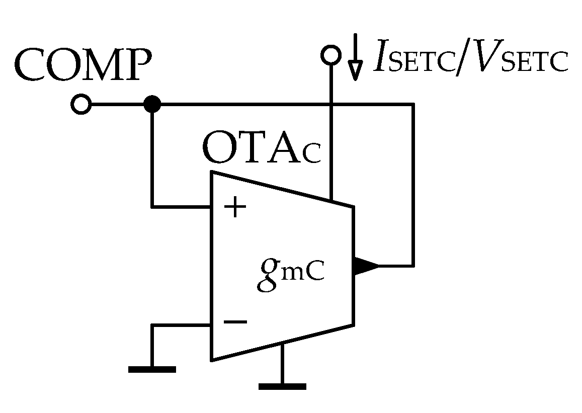
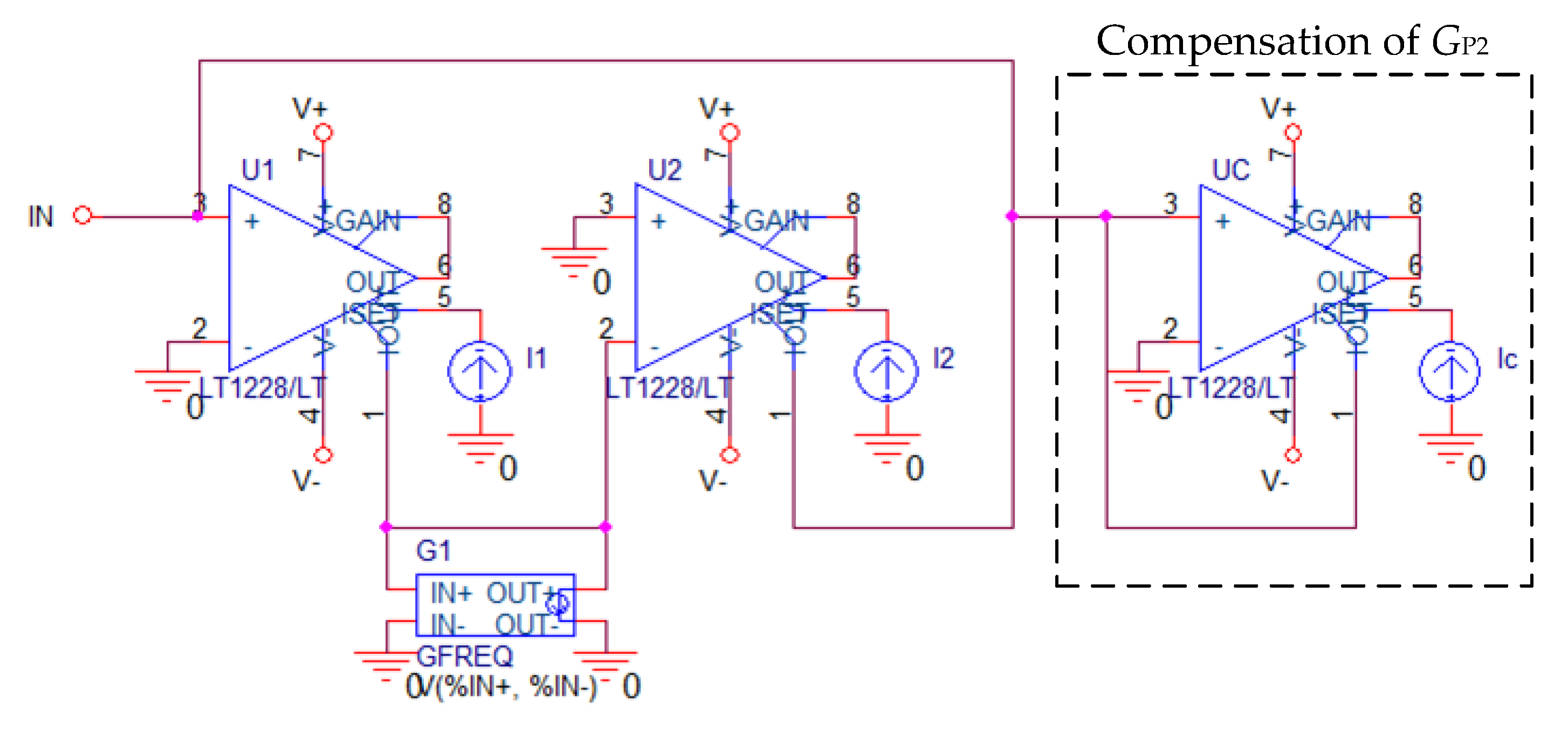
2.2.2. Compensation of Parasitic Conductance

When a parasitic conductance of a gyrator node is to be decreased as described in the previous section, a simple compensation circuit with negative input conductance, shown in Figure 6, can be used. This circuit is connected with its COMP terminal to the node where the parasitic conductance is to be compensated.
The conductance of the COMP terminal relative to ground equals to
G COMP = g mC + G P
and can be set to an appropriate negative value by the electronic setting of gmC. Here GP is the total parasitic conductance of OTAC input and output terminals. If the implementation of OTAC is identical with the OTAs of the gyrator, all the parasitic conductances are equal (GP = GP1 = GP2). From (8), it is apparent that when the admittance GP1 is compensated in this way to almost zero value, the cut-off frequency ωGP1 can be theoretically shifted to very low values, and the maximum magnitude of the gyrator input admittance can be increased significantly. However, the demands on the accuracy of the compensation circuit increase, and it is important to prevent reaching a negative conductance of the node. The conductance GP2 is worth to be compensated when it affects the gyrator input admittance at high frequencies between ωGP2 and ωCP2, i.e., when the solid line (and not the dashed line) in Figure 5 holds. Remember that when α tends to unity, the conductance GP2 is an important damping factor of the above-mentioned LC resonance, and thus, it cannot be excessively reduced.
It should also be noted that when connecting the circuit in Figure 6 to a gyrator node, the parasitic capacitance of this node increases by the own parasitic capacitance of the compensation circuit, which is equal to CP1 and CP2, assuming that all OTAs are the same. Thus, it is necessary to take this property into account in the relations containing the parasitic capacitance of the node being compensated. Note that the circuit in Figure 6 cannot be used for compensating the gyrator parasitic capacitance.

2.2.3. Dynamic Properties

Next to the non-ideal frequency analysis, it is also important to investigate the dynamic properties of the gyrator such that the amplifiers operate in linear mode and the maximum voltage and current values of their terminals are not exceeded. As far as common OTAs are concerned, the most limiting is the non-linearity of their input transistor stage, which takes effect already at differential input voltages of several tens of millivolts. Let us denote the maximum allowed amplitude of OTA input voltage for linear operation VOTA,MAX. The output drive current of OTA is also limited to a maximum value IOTA,MAX; whereas, it holds IOTA,MAX = gmVOTA,MAX. The value of VOTA,MAX, and also maximum allowable transconductance gm can be determined from the respective OTA documentation. The following two conditions must be met to avoid the non-linear operation of the gyrator:
  • The gyrator input voltage VIN must not be higher than the allowed input voltage range of OTA1 VOTA1,MAX
    V IN V OTA 1 , MAX .
  • The second condition for VIN provides that the voltage swing across the gyrator loading admittance Y does not exceed the maximum possible OTA2 input voltage VOTA2,MAX
    V IN g m 2 V OTA 2 , MAX | Y IN | .
Apparently, the allowed VIN according to (14) changes with frequency. It reaches the minimum value at the lowest operating frequency where |YIN| is maximal. It can be concluded that the gyrator input voltage VIN must meet both the conditions (13) and (14) simultaneously when the linear operation of both OTAs is required. If the conditions for maximum gyrator input current IIN are required, they can be easily derived from (13) and (14) by substituting VIN = IIN/|YIN|.

2.3. Guidelines for Setting of Gyrator Parameters

Practical guidelines for gyrator parameter design were compiled based on the above observations. By following these rules, in addition to the correct input admittance, we also ensure its highest possible frequency and magnitude range and prevent the active elements from non-linear operation and overloading. The starting point of the design is the required value of input admittance YIN specified, e.g., by FIN and α, or magnitude at specific frequency and phase, see (5) and (6). The first set of guidelines (labeled A) can be used if there is available any value of the fractance F of the FO capacitor loading the gyrator.
A.1.
Choose the same gm1 and gm2 as the highest possible values for the correct functionality of the selected OTAs. The maximum transconductance values can be found in OTA documentation and are usually several hundreds of μS for CMOS and several tens of mS for BJT implementations. The choice of maximal transconductances extends the operating band to low frequencies. If this is not a priority, choose the transconductances equal to the required input admittance magnitude at the commonly used frequency, e.g., at the geometric mean of the operating band.
A.2.
Calculate the value of fractance F from the magnitude part of (6). If the value of F turns out too high for implementation, then it is possible to use the next set of rules labeled B, where a lower value of F can be set at the beginning. If F turns out too small, the only solution is to choose OTAs with higher maximum transconductances.
A.3.
Check the frequency range of the correct functionality of the gyrator, according to (8), (9), or (11). If the range is not sufficient, consider reducing parasitic conductance(s) by the compensation described in Section 2.2.2.
A.4.
To prevent the OTAs from the non-linear operation, ensure that the magnitude of the gyrator input voltage VIN meets both the conditions (13) and (14) simultaneously in the operating frequency band.
The next set of rules (labeled B) is applicable if a specific value of the fractance F should be set at the beginning.
B.1.
Set a specific value of the fractance F. If a cut-off frequency ωGP1 should be reached without compensation of parasitic conductance GP1, the selected value F must be at least as determined from (8).
B.2.
Determine the required product gm1gm2 for the selected F and given FIN from the magnitude part of (6). Evaluate whether the product is achievable by the selected OTAs. If not, F must be reduced for the design to continue (regardless of fulfilling (8) in the previous step).
B.3.
Choose gm2 as the highest possible value for the proper functionality of the selected OTA2.
B.4.
Calculate gm1 from the magnitude part of (6). If the ratio gm1/gm2 turns out excessively low, then it is possible to decrease gm2 and an increase gm1 such that their product remains the same. However, keep in mind that decreasing gm2 may decrease the allowed gyrator input voltage, according to (14).
B.5.
Check the frequency range of the correct functionality of the gyrator, according to (8), (9), or (11). If the range is not sufficient, consider reducing parasitic conductance(s) by the compensation described in Section 2.2.2.
B.6.
To prevent the OTAs from the non-linear operation, ensure that the magnitude of the gyrator input voltage VIN meets both the conditions (13) and (14) simultaneously in the operating frequency band.
To add more clarity, a flowchart of the above guidelines for the setting of gyrator parameters is enclosed in Figure 7.

2.4. Differential (Floating) Version of the Gyrator

If the OTA2 with differential (balanced) output is available, it is possible to easily obtain a differential gyrator with floating input according to Figure 8. The describing relations (4) to (6) remain valid; however, the parasitics GP2 and CP2 must be considered with halved values GP2/2 and CP2/2 in the analyses, as the OTA terminal parasitic elements are connected in series here (through ground). These reduced parasitic values improve the functionality of the gyrator at high frequencies. Another advantage of the floating gyrator is that the loading element Y remains grounded.

3. Simulation Results and Discussion

To verify the presented theoretical studies and also demonstrate the design optimization, the computer simulation of the gyrator behavior was carried out using OrCAD PSpice software. The commercially available integrated circuit LT1228 [26] was used as OTA to enable the readers the possibility of reproducing the results. This element provides transconductance gm controlled by an external DC current ISET; whereas, it holds gm = 10ISET. An analysis of the LT1228 PSpice model parasitic properties revealed that the conductance of input pins GP,IN is variable and depends on gm with the relation GP,IN ≈ 0.005gm. It is, therefore, necessary to take into account that the functionality of the gyrator will be more affected by the parasitic conductance at higher values of gm. The input parasitic conductance is not included in the LT1228 PSpice model, i.e., it is considered zero. The parasitic conductance GP,OUT of output pin is approximately 0.23 nS and can be neglected in comparison with GP,IN for common values of gm. The parasitic output capacitance is 5.2 pF. Thus, the modeled parasitic conductances GP1 and GP2 of the gyrator correspond to 0.005gm2 and 0.005gm1, respectively, and both the parasitic capacitances CP1 and CP2 are 5.2 pF.

3.1. Gyrator Simulation and Optimization

The input admittance magnitude of the gyrator chosen in this subsection is |YIN| = 10 mS at 1 kHz, and the orders α are 0.25, 0.5, 0.75, 1, i.e., three of them representing FO and one classic inductance simulator. Two sets of element parameters will be used for demonstration. The first set (labeled set 1) will be designed only to provide the required input admittance, regardless of the previously proposed recommendations concerning the wide frequency and magnitude range. Then, the elements of set 2 will be designed regarding these recommendations to demonstrate the optimization of admittance characteristics. The schematic of the gyrator in the OrCAD Capture editor is depicted in Figure 9. Unless otherwise noted, the circuit is considered without the compensation part indicated by the dashed box.
To show solely the influence of parasitic properties of the employed OTAs, ideal FO capacitors were used as gyrator load Y. These elements were modeled in OrCAD by GFREQ part representing voltage-controlled current source described by a table of frequency response in magnitude and phase domain [27]. Interpolation is performed between the entries; whereas, magnitude is interpolated logarithmically and phase linearly. By interconnecting the input and output of the GFREQ part as displayed in Figure 9, the resulting element admittance is described by a series of (input frequency in Hz, magnitude in dB, phase in degrees) triplets.
The OTA transconductances are chosen gm1 = gm2 = 1 mS in the first set of circuit parameters. To obtain the required |YIN| = 10 mS at 1 kHz, the magnitude of loading admittance according to (4) is |Y| = 0.1 mS at 1 kHz. The orders of the loading admittance are α = 0.25, 0.5, 0.75, 1, i.e., three of them FO and one classic capacitor. The summary of this first set of element parameters is given in Table 1, along with the expected lower and upper cut-off frequencies determined by the relations (8), (9), and (11).
The second set of gyrator element parameters is designed following rules A from Section 2.3, which should provide optimization of both the frequency and dynamic range of the gyrator input admittance. The maximum transconductances of LT1228 OTA are chosen based on the datasheet gm1 = gm2 = 20 mS. To obtain the required |YIN| = 10 mS at 1 kHz, the magnitude of loading admittance is |Y| = 40 mS at 1 kHz. The summary of this second set of element parameters with the expected cut-off frequency values is given in Table 2.
The values of lower cut-off frequency fGP1 for the second set are lower than for the first set, as expected. As seen in the last column of Table 2 (values that are not in parentheses), the upper cut-off frequencies decreased for α = 0.75 and 1 compared with Table 1. This bandwidth degradation is caused by the parasitic conductance GP2, which raised from 5 μS for the first element set to 100 μS for the second set, due to increasing the transconductance gm1 (it holds GP2 = 0.005gm1). The parasitic conductance GP2 can be decreased as described in Section 2.2.2, resulting in an increase of the upper cut-off frequency. The compensation circuit with negative admittance utilized for this purpose is marked with the dashed box in Figure 9. The transconductance gmC of the OTA in the compensation circuit was set to 99.5 μS, which leads to GP2 ≈ 1 μS and that is an even better value than for the first set of elements. It should be taken into account that the compensation circuit causes a doubling of the parasitic capacitance CP2, therefore, the results after compensation have improved, but still do not reach the values as for the first set, see the frequencies in the last column of Table 2 in parentheses.
The simulated magnitude and phase-frequency characteristics of the gyrator input admittance are depicted in Figure 10, Figure 11, Figure 12 and Figure 13 for the α values 0.25, 0.5, 0.75, 1, respectively. The solid black lines are valid for the first set of circuit parameters, the dotted green lines for the second set, and the dashed blue lines indicate ideal results. It is worth to mention again that the simulations in this subsection are performed with ideal FO capacitor loading the gyrator to solely illustrate the effect of OTA non-ideal properties. Common FO capacitors emulated by RC structures of reasonable complexity have limited accuracy in a limited frequency band [28], which would unnecessarily degrade the results, and it would not be clear whether the distortion is caused by non-idealities of OTA or FO capacitor.
The simulated admittance characteristics in Figure 10, Figure 11, Figure 12 and Figure 13 are in accordance with the Bode plots in Figure 5, and the important asymptotic magnitude and phase values are confirmed. The limited frequency band of the correct functionality of the gyrator can be observed, and the simulated magnitude cut-off frequencies correspond to the expected values from Table 1 and Table 2. Considering the maximum phase error ±2 degrees, the useful frequency ranges for the designed FO inductance simulators are listed in Table 3.
Furthermore, the simulations confirm that the admittance magnitude at low frequencies is limited to the value gm1gm2/GP1, which is 200 mS for the first set of elements and 4 S for the second one. The constant magnitude section between ωGP2 and ωCP2 is not apparent in the simulations as the value GP2 is too low to take effect. This section would be visible for the set 2 magnitudes with α values 0.75 and 1 if no GP2 compensation were applied. The effect of the additional capacitance of the compensation circuit is demonstrated in Figure 12a and Figure 13a by increasing the magnitude at high frequencies compared to set 1 results. The simulated results also confirm that the bandwidth of correct gyrator operation increases as α decreases.

3.2. Inductance Simulator for Fractional-Order Respiratory Model

Fractional-order electrical circuit models are useful in modeling the mechanical impedance of the respiratory system [11,12]. Mechanical impedance of the human respiratory system can be represented by an equivalent model given in Figure 14.
The impedance of this system is expressed as
Z ( s ) = s α L + R + 1 s β C .
The experimentally extracted values of (15) for human respiratory system are L = 0.0193 H·sec0.5313, α = 0.4687, R = 0.0147 Ω, C = 0.9921 F·sec0.2729, β = 0.7271 and the frequency range of the model validity is 4 Hz to 48 Hz [12]. The FO inductor with impedance sαL included in this model will be implemented by the discussed OTA-based gyrator in this section as an example of its practical utilization. The grounded version of the model will be demonstrated, as the floating version requires OTA with differential output (see Figure 8), which is not the case of the used integrated circuit LT1228. The value of FIN in accordance with (5) and (15) is equal to 1/L = 51.81 H1·sec0.5313. This value represents a very high admittance magnitude of 11.43 S at the corner frequency of 4 Hz, and the implementation of the inductor is therefore challenging.
Rules A, in Section 2.3, will be used to design the gyrator element parameters. The transconductances are chosen gm1 = gm2 = 20 mS again as the maximum possible values for LT1228. To obtain the required |YIN| = 11.43 S at 4 Hz, the magnitude of loading admittance is |Y| = 34.987 μS at 4 Hz, its order is α = 0.4687, and F = 7.72 μF·sec0.5313. Thanks to the narrow frequency band (4 Hz to 48 Hz) compared to the simulations in the previous subsection and to implement it by available components, the FO capacitor loading the gyrator was emulated by the Valsa structure [29] containing standard resistors and capacitors, as shown in Figure 15. Another reason to employ this RC emulator is that the GFREQ part cannot be used in transient analysis, which will demonstrate dynamic optimization of the gyrator at the end of this section. The element values of the Valsa RC circuit computed by the method described in Reference [29] for the mentioned values α, F, maximum phase error ±0.6 degrees, and the frequency range 0.8 Hz to 240 Hz (to have sufficient margin) are listed in Table 4.
The admittance magnitude and phase characteristics of the emulated FO capacitor (solid black lines) and the ideal values (dashed blue lines) are presented in Figure 16. It can be observed that the circuit operates according to the above-mentioned required parameters.
The gyrator lower cut-off frequency computed by (8) is fGP1 = 37.6 Hz, which is not sufficiently low, as the FO inductor should operate from 4 Hz. This limitation is caused by the parasitic conductance GP1 = 100 μS, which will be decreased by the circuit with negative admittance. Thus, now the compensation circuit in the dashed box in Figure 9 is replaced and connected in parallel with the FO capacitor loading the gyrator. The transconductance gmC is 97 μS, and it leads to GP1 ≈ 3.5 μS. The expected cut-off frequency after compensation is fGP1 ≈ 0.03 Hz and maximum obtainable input admittance magnitude gm1gm2/GP1 ≈ 115 S, which is ten times higher than the required admittance magnitude of the implemented FO inductor at 4 Hz. Note that these values are valid for the gyrator loaded with an ideal FO capacitor. It can be expected that the results will be degraded after connecting the emulator of FO capacitor, which has limited accuracy of its admittance.
The simulated magnitude and phase frequency characteristics of the gyrator input admittance are shown in Figure 17. The solid black lines represent simulated results, and the blue lines indicate ideal values with the solid part denoting the frequency band of interest, i.e., 4 Hz to 48 Hz.
In this frequency band, the maximum absolute magnitude error is 1.5 S, and phase error is 3.1 degrees when comparing the simulated results with the ideal ones. It is apparent that the error increases at the lower bound of the frequency band. The magnitude error can be easily corrected by fine increasing the product gm1gm2, which can be set electronically. The phase deviation can be reduced by fine-tuning the transconductance gmC; however, the demands on the accuracy of setting gmC increase, and it is important to prevent overcompensating GP1 to a negative value.
The dynamic optimization was also performed based on the conditions introduced in Section 2.2.3. When following these conditions, only allowed voltages and currents will appear in the gyrator structure, and the amplifiers will operate in linear range without overloading. The maximum input voltage amplitude of both OTAs for their linear operation is considered VOTA,MAX = 50 mV. The maximum input voltage of the gyrator can be determined as the maximum value of VIN that meets both conditions (13) and (14) simultaneously. The maximum input current can then be computed using IIN = VIN|YIN|. The following Table 5 shows the maximum allowed amplitudes of voltages and currents at the input (VIN, IIN) of the gyrator, ensuring linear operation of both OTAs for three frequency points, in the beginning, inside (at 25 Hz), and at the end of the operating band. The computed amplitudes of voltages and currents at the gyrator load (VLOAD, ILOAD) are also stated.
Applying the rules for dynamic optimization, the transient simulation with the maximum allowed input current amplitude IIN = 1 mA and frequency 25 Hz was carried out, and the resulting current and voltage waveforms are presented in Figure 18. The voltages are relative to ground, and currents are considered positive when flowing into the gyrator (IIN) and into the loading FO capacitor (ILOAD).
The delay between input current and voltage found by the simulation is 4.53 msec; the corresponding α is 0.453 which is close to the required value of 0.4687. The amplitude of the simulated input voltage 224 μV is slightly higher than the value 206 μV according to Table 5. This matches the fact that the gyrator input admittance magnitude is lower than the target value, which is also observed in Figure 17a. The current through the gyrator load reaches 4.42 μA, also slightly higher than the expected 4.13 μA. The simulated load voltage of 50.8 mV is almost equal to the value of 50 mV in Table 5. It is verified that the voltage and current amplitudes of the gyrator are optimized and do not cause the non-linear function of active elements.
It should be noted here that this particular FO inductor for the respiratory model is characterized by uncommonly high admittance magnitude at low frequency. Therefore, when it is excited by a current of 1 mA, a very small voltage of less than 300 μV appears at its terminals. Moreover, the gyrator load current is very small, of the order of microamperes. Thus, in the case of real implementation and measurement, these small electrical signals would probably be disturbed by noise. In this case, it would be more appropriate to use OTAs with higher transconductance and maximum output current or at least with a higher maximum voltage and current at the same transconductance. In general, it is suitable for the gyrator to select OTAs with transconductance values comparable to the required input admittance magnitude at the operating frequency. This will provide comparable voltage amplitudes at the input and load of the gyrator, as well as comparable currents at the same points.

4. Conclusions

In this article, we presented a comprehensive analysis of the OTA-based gyrator implementing FO inductor to identify and evaluate the limitations caused by the active element real properties, particularly affecting the operational frequency bandwidth, range of the obtainable input admittance, and signal dynamic range. Based on this analysis, design recommendations were provided to overcome or minimize these limitations caused by the real properties of the assumed active elements. During the gyrator design, it is important to set sufficiently large OTA transconductances that are preferably comparable with the required gyrator input admittance magnitude. This also leads to sufficiently large fractance F, which reduces the circuit sensitivity to the parasitics GP1 and CP1. To further improve the properties of the gyrator, it is possible to suppress the parasitic conductances by connecting a shunt active compensation circuit with negative conductance also designed with OTA. It is important to take into account that the FO capacitor connected to the gyrator also has limited accuracy and frequency bandwidth. Therefore, it is advisable to match the operating frequency bands of the FO capacitor and the gyrator to avoid unnecessary degradation of the FO inductor function. The proposed optimization steps were verified by OrCAD PSpice simulations while designing FO inductors with different orders; whereas, the FO inductor 0.0193 H·sec0.5313 with order 0.4687 being part of fractional-order respiratory model operating in the frequency range 4 Hz to 48 Hz was also successfully emulated.

Author Contributions

Conceptualization, N.H.; Formal analysis, D.K. and J.K.; Funding acquisition, J.K.; Investigation, D.K., N.H. and R.S.; Methodology, D.K.; Validation, J.D. and R.S.; Visualization, J.D.; Writing—original draft, D.K. and J.K. All authors have read and agreed to the published version of the manuscript.

Funding

This research and the APC were funded by The Czech Science Foundation, grant number 19-24585S.

Institutional Review Board Statement

Not applicable.

Informed Consent Statement

Not applicable.

Data Availability Statement

Data is contained within the article.

Acknowledgments

This article is based upon work from COST Action CA15225, a network supported by COST (European Cooperation in Science and Technology).

Conflicts of Interest

The authors declare no conflict of interest. The funders had no role in the design of the study; in the collection, analyses, or interpretation of data; in the writing of the manuscript, or in the decision to publish the results.

References

  1. Kubanek, D.; Koton, J.; Dvorak, J.; Herencsar, N.; Sotner, R. Analysis of OTA-Based Gyrator Implementing Fractional-Order Inductor. In Proceedings of the 43rd International Conference on Telecommunications and Signal Processing (TSP), Milan, Italy, 7–9 July 2020; pp. 583–588. [Google Scholar] [CrossRef]
  2. Elwakil, A. Fractional-order circuits and systems: An emerging interdisciplinary research area. IEEE Circuits Syst. Mag. 2010, 10, 40–50. [Google Scholar] [CrossRef]
  3. Tepljakov, A. Fractional-Order Modeling and Control of Dynamic Systems; Springer International Publishing: Berlin/Heidelberg, Germany, 2017. [Google Scholar] [CrossRef]
  4. Shah, Z.M.; Kathjoo, M.Y.; Khanday, F.A.; Biswas, K.; Psychalinos, C. A survey of single and multi-component Fractional-Order Elements (FOEs) and their applications. Microelectron. J. 2019, 84, 9–25. [Google Scholar] [CrossRef]
  5. Adhikary, A.; Khanra, M.; Sen, S.; Biswas, K. Realization of a carbon nanotube based electrochemical fractor. In Proceedings of the 2015 IEEE International Symposium on Circuits and Systems (ISCAS), Lisbon, Portugal, 24–27 May 2015; pp. 2329–2332. [Google Scholar] [CrossRef]
  6. Adhikary, A.; Sen, S.; Biswas, K. Practical realization of tunable fractional-order parallel resonator and fractional-order filters. IEEE Trans. Circ. Syst. I Fundam. Theory Appl. 2016, 63, 1142–1151. [Google Scholar] [CrossRef]
  7. Adhikary, A.; Sen, S.; Biswas, K. Design and hardware realization of a tunable fractional-order series resonator with high quality factor. Circ. Syst. Signal Process. 2016, 36, 3457–3476. [Google Scholar] [CrossRef]
  8. Tsirimokou, G.; Psychalinos, C.; Elwakil, A.S.; Salama, K.N. Electronically tunable fully integrated fractional-order resonator. IEEE Trans. Circ. Syst. II 2018, 65, 166–170. [Google Scholar] [CrossRef] [Green Version]
  9. Radwan, A.G.; Fouda, M.E. Optimization of fractional-order RLC filters. Circuits Syst. Signal Process. 2013, 32, 2097–2118. [Google Scholar] [CrossRef]
  10. Freeborn, T.J.; Maundy, B.; Elwakil, A.S. Fractional resonance based RLβCα filters. Math. Probl. Eng. 2013, 2013, 1–10. [Google Scholar] [CrossRef] [Green Version]
  11. Ionescu, C.M.; Keyser, R.D. Time domain validation of a fractional order model for human respiratory system. In Proceedings of the 14th IEEE Mediterranean Electrotechnical Conference, Ajaccio, France, 5–7 May 2008; pp. 89–95. [Google Scholar] [CrossRef]
  12. Freeborn, T.J. A survey of fractional-order circuit models for biology and biomedicine. IEEE J. Emerg. Select. Top. Circ. Syst. 2013, 3, 416–424. [Google Scholar] [CrossRef]
  13. Schäfer, I.; Krüger, K. Modelling of lossy coils using fractional derivatives. J. Phys. D Appl. Phys. 2008, 41, 045001. [Google Scholar] [CrossRef]
  14. Zhang, G.; Ou, Z.; Qu, L. A Fractional-Order Element (FOE)-Based Approach to Wireless Power Transmission for Frequency Reduction and Output Power Quality Improvement. Electronics 2019, 8, 1029. [Google Scholar] [CrossRef] [Green Version]
  15. Kuo, F. Network Analysis and Synthesis; John Wiley & Sons Inc: New York, NY, USA, 1966. [Google Scholar]
  16. Valkenburg, M.E. Network Analysis; Prentice Hall: Toronto, ON, Canada, 1974. [Google Scholar]
  17. Kartci, A.; Agambayev, A.; Farhat, M.; Herencsar, N.; Brancik, L.; Bagci, H.; Salama, K.N. Synthesis and optimization of fractional-order elements using a genetic algorithm. IEEE Access 2019, 7, 80233–80246. [Google Scholar] [CrossRef]
  18. Tsirimokou, G.; Kartci, A.; Koton, J.; Herencsar, N.; Psychalinos, C. Comparative Study of Discrete Component Realizations of Fractional-Order Capacitor and Inductor Active Emulators. J. Circuits Syst. Comput. 2018, 27, 1–26. [Google Scholar] [CrossRef]
  19. Deliyannis, T.; Sun, Y.; Fidler, J.K. Continuous-Time Active Filter Design; CRC Press: Boca Raton, CA, USA, 1999. [Google Scholar]
  20. Adhikary, A.; Sen, P.; Sen, S.; Biswas, K. Design and Performance Study of Dynamic Fractors in Any of the Four Quadrants. Circuits Syst. Signal Process. 2016, 35, 1909–1932. [Google Scholar] [CrossRef]
  21. Adhikary, A.; Choudhary, S.; Sen, S. Optimal Design for Realizing a Grounded Fractional Order Inductor Using GIC. IEEE Trans. Circuits Syst. I Reg. Pap. 2018, 65, 2411–2421. [Google Scholar] [CrossRef]
  22. Khattab, K.H.; Madian, A.H.; Radwan, A.G. CFOA-based fractional order simulated inductor. In Proceedings of the 2016 IEEE 59th International Midwest Symposium on Circuits and Systems (MWSCAS), Abu Dhabi, UAE, 16–19 October 2016; pp. 1–4. [Google Scholar] [CrossRef]
  23. Geiger, R.L.; Sánchez-Sinencio, E. Active filter design using operational transconductance amplifiers: A tutorial. IEEE Circuits Devices Mag. 1985, 1, 20–32. [Google Scholar] [CrossRef]
  24. Sotner, R.; Jerabek, J.; Kartci, A.; Domansky, O.; Herencsar, N.; Kledrowetz, V.; Alagoz, B.B.; Yeroglu, C. Electronically reconfigurable two-path fractional-order PI/D controller employing constant phase blocks based on bilinear segments using CMOS modified current differencing unit. Microelectron. J. 2019, 86, 114–129. [Google Scholar] [CrossRef]
  25. Bakken, T.; Choma, J. Gyrator-Based Synthesis of Active On-Chip Inductances. Analog Integr. Circuits Signal Process. 2003, 34, 171–181. [Google Scholar] [CrossRef]
  26. LT1228 100 MHz Current Feedback Amplifier with DC Gain Control; Datasheet; Linear Technology: Milpitas, CA, USA, 2012.
  27. Cadence Design Systems. PSpice® User’s Guide; Cadence Design Systems: Portland, OR, USA, 2000. [Google Scholar]
  28. Tsirimokou, G. A Systematic Procedure for Deriving RC Networks of Fractional-Order Elements Emulators Using MATLAB. Int. J. Electron. Commun. 2017, 78, 7–14. [Google Scholar] [CrossRef]
  29. Valsa, J.; Vlach, J. RC models of a constant phase element. Int. J. Circuit. Theory Appl. 2013, 41, 59–67. [Google Scholar] [CrossRef]
Figure 1. OTA schematic symbol.
Applsci 11 00291 g001
Figure 2. Gyrator with two OTAs.
Applsci 11 00291 g002
Figure 3. Gyrator with OTA parasitic properties.
Applsci 11 00291 g003
Figure 4. Substitute circuit providing the input admittance (7); the relations in the schematic express admittances of the particular elements.
Applsci 11 00291 g004
Figure 5. Bode plots of (a) magnitude and (b) phase admittance characteristics according to (7). Blue parts denote ideal function without the influence of parasitics.
Applsci 11 00291 g005
Figure 6. Circuit with grounded negative conductance at terminal COMP.
Applsci 11 00291 g006
Figure 7. Flowchart of the setting of gyrator parameters.
Applsci 11 00291 g007
Figure 8. A differential (floating) variant of the gyrator from Figure 2.
Applsci 11 00291 g008
Figure 9. OrCAD Capture schematic of the simulated gyrator.
Applsci 11 00291 g009
Figure 10. Simulated magnitude (a) and phase (b) characteristics of gyrator input admittance for α = 0.25.
Applsci 11 00291 g010
Figure 11. Simulated magnitude (a) and phase (b) characteristics of gyrator input admittance for α = 0.5.
Applsci 11 00291 g011
Figure 12. Simulated magnitude (a) and phase (b) characteristics of gyrator input admittance for α = 0.75.
Applsci 11 00291 g012aApplsci 11 00291 g012b
Figure 13. Simulated magnitude (a) and phase (b) characteristics of gyrator input admittance for α = 1.
Applsci 11 00291 g013
Figure 14. FO impedance model of the human respiratory system [11].
Applsci 11 00291 g014
Figure 15. Valsa RC circuit to emulate FO capacitor.
Applsci 11 00291 g015
Figure 16. Admittance magnitude (a) and phase (b) characteristics of the approximated FO capacitor from Figure 15.
Applsci 11 00291 g016
Figure 17. Simulated magnitude (a) and phase (b) characteristics of gyrator input admittance implementing FO inductor for the respiratory model.
Applsci 11 00291 g017
Figure 18. Optimized voltage and current waveforms at the input (a) and load (b) of gyrator excited with 1 mA current amplitude.
Applsci 11 00291 g018
Table 1. First set of element parameters for simulation of the circuit in Figure 9 and its expected cut-off frequencies.
gm1 = gm2
(mS)
αF
(F·secα–1)
GFREQ TABLEfGP1
(Hz)
min{fGP2, fCP2′}
(Hz)
10.2511.23 μ(10m,-105,22.5) (100meg,-55,22.5)6.25 m24.5 M
10.51.262 μ(10m,-130,45) (100meg,-30,45)2.54.54 M
10.75141.7 n(10m,-155,67.5) (100meg,-5,67.5)18.41.36 M
1115.92 nClassic capacitor 15.92 nF instead of GFREQ 50553 k
Table 2. The second set of element parameters for simulation of the circuit in Figure 9 and its expected cut-off frequencies.
gm1 = gm2
(mS)
αF
(F·secα–1)
GFREQ TABLEfGP1
(Hz)
min{fGP2, fCP2′}
(Hz)
200.254.493 m(10m,-52.96,22.5) (100meg,-2.96,22.5)39.1 n24.5 M
200.5504.6 μ(10m,-77.96,45) (100meg,22.04,45)6.25 m4.54 M
200.7556.68 μ(10m,-102.96,67.5) (100meg,47.04,67.5)339 m464 k (918 k)
2016.366 μClassic capacitor 6.366 μF instead of GFREQ 2.5100 k (391 k)
Table 3. Comparison of frequency ranges of FO inductance simulators for maximum phase error ±2 degrees.
Setα = 0.25α = 0.5α = 0.75α = 1
162 Hz–395 kHz950–1 MHz1.44 kHz–226 kHz1.45 kHz–72 kHz
20.4 mHz–2.43 MHz2.4 Hz–24.6 kHz26 Hz–173 kHz71 Hz–148 kHz
Table 4. Resistances and capacitances in the circuit from Figure 15 (α = 0.4687, F = 7.72 μF·sec−0.5313).
R0 (kΩ)R1 (kΩ)R2 (kΩ)R3 (kΩ)R4 (kΩ)
15010039166.8
C0 (nF)C1 (μF)C2 (nF)C3 (nF)C4 (nF)
562750270100
Table 5. Maximum allowed voltages and currents in the gyrator structure.
f (Hz)VIN (μV)IIN (mA)VLOAD (mV)ILOAD (μA)
487.51501.75
252061504.13
482801505.61
Publisher’s Note: MDPI stays neutral with regard to jurisdictional claims in published maps and institutional affiliations.

