Article

A Novel Cross-Latch Shift Register Scheme for Low Power Applications

1
Electronic Engineering, National Yunlin University of Science and Technology, Yunlin County, Douliu City 64002, Taiwan
2
Information and Communication Engineering, Chaoyang University of Technology, Wufeng District, Taichung City, Taichung 413310, Taiwan
*
Author to whom correspondence should be addressed.
Appl. Sci. 2021, 11(1), 129; https://doi.org/10.3390/app11010129
Submission received: 22 November 2020 / Revised: 21 December 2020 / Accepted: 23 December 2020 / Published: 25 December 2020
(This article belongs to the Section Electrical, Electronics and Communications Engineering)

Abstract

:
The conventional shift register consists of master and slave (MS) latches with each latch receiving the data from the previous stage. Therefore, the same data are stored in two latches separately. It leads to consuming more electrical power and occupying more layout area, which is not satisfactory to most circuit designers. To solve this issue, a novel cross-latch shift register (CLSR) scheme is proposed. It significantly reduced the number of transistors needed for a 256-bit shifter register by 48.33% as compared with the conventional MS latch design. To further verify its functions, this CLSR was implemented by using TSMC 40 nm CMOS process standard technology. The simulation results reveal that the proposed CLSR reduced the average power consumption by 36%, cut the leakage power by 60.53%, and eliminated layout area by 34.76% at a supply voltage of 0.9 V with an operating frequency of 250 MHz, as compared with the MS latch.

1. Introduction

The shift register has been commonly used in various digital circuits for decades. This circuit block can be applied in conversion between serial and parallel interfaces during data transmission, and it can be used as a delay circuit too. The shift register is a key component in digital circuits and is generally used in active-matrix displays, sensors, memories, communication receivers, and real-time image processing chips [1,2,3,4,5,6,7,8]. The shrinking feature size of process technology has enhanced the potential performance of electronic devices, and the capacity of shift registers has increased significantly. Therefore, asking for less overhead integrated circuitry layout area [9,10,11,12] and less power consumption [9,11,13,14,15,16,17,18,19,20,21,22,23,24,25,26] in the shift registers design then becomes more important with the capacity increasing [27].
The conventional architecture of a shift register consists of N-bit flip-flops connected in series. Circuit implementation in such architecture is fast and efficient. However, requesting less overhead layout area and less power consumption still cannot be fulfilled. Additionally, in master and slave (MS) latch architecture, the same data are stored in two latches during one clock cycle. Hence, the MS latch tends to exhibit redundant area and dissipate more electric power. Obviously, if shift registers are implemented by MS latches without a compensation circuit, the data will be transmitted to multiple outputs at the same time and may result in a malfunction. Recently, B. D. Yang proposed a shift register that employed a pulse-latched methodology to solve this issue [27]. The concept behind this reported shift register is using a sub-shift register with an N-bit latch and using an N + 1-bit clock pulse generator to generate an N + 1 non-overlapping clock in one clock cycle to avoid data duplication. Although in this work, the author employed one additional latch in each sub-register to store 1-bit temporary data to solve the timing problem between pulsed latches; however, the circuitry complexity was increased as well. The adoption of multiple non-overlap delayed pulsed clock signals limits the circuit operating clock frequency. Moreover, this shift register uses N sub-shift registers to increase the number of latches at the same time. In [27], the author proposed a latch controlled by a pulse generator. This is similar to the behavior of a trigger flip-flop, and the area can be decreased by sharing a pulse generator so that it is suitable for high-speed application. However, the pulse width is difficult to control due to the process variations. Based upon the above discussions, the simultaneous requests for the elimination of the integrated circuit layout area and the reduction of electrical power consumption still could not be realized in the reported work. To solve that issue, in this study, a cross-latch scheme combined with a flip-flop design is proposed to achieve area saving under low operation voltage.
To overcome the current drawbacks of the conventional MS latch design, in this paper, we propose a novel cross-latch shift register (CLSR) scheme. The proposed CLSR requires only one latch to perform the same functions as those of the MS latches in a conventional shift register. Thus, the proposed CLSR consumes less power and occupies less layout area by reducing the number of transistors.
Details of the proposed configuration are explained in the next section. In Section 2, the principle of the proposed cross-latch shift register (CLSR) is discussed. Experimental validation and a mechanism depiction for the proposed CLSR are presented in Section 3.

2. The Proposed Cross-Latch Shift Register (CLSR) Design

Figure 1 shows the process of data transmission for a conventional shift register under different clock signals (CLK = 1 and CLK = 0). As shown in Figure 1a, for a shift register with a positive edge triggered flip-flop, when CLK = 0 at the first stage flip-flop (FF0), the master latch (M0) is opened and receives the input data while the slave latch (S0) is closed and stores the previous data. At the same time, in the second stage flip-flop (FF1), the master latch (M1) will track the data stored in the slave latch (S0) of FF0. Likewise, as shown in Figure 1b, when CLK = 1, the slave latch of each flip-flop will track the data in the master latch and send it to the output. According to a data transmission analysis, it can be observed that when CLK = 0, the slave latch (S0) of FF0 and master latch (M1) of FF1 store the same data. When CLK = 1, each flip-flop holds the same data in the master and slave latches, respectively. This situation leads to storage of redundant data in many latches. Implementing and keeping this state may consume extra electrical power and may occupy more overhead integrated circuitry layout area. Note that in addition to showing the traditional transmission gate flip-flop (TGFF), Figure 2 also includes three recently proposed low-power FF designs [28,29,30]. Figure 2b shows the adaptive coupling (AC) flip-flop design [28]. Unlike the traditional MS latch-based design, this design uses a differential latch structure with pass transistor logic to achieve true single-phase clock (TSPC) operation. To overcome the effects of process variation on the master latch, a pair of level recovery circuits were inserted into the cross-coupled path. In this design, the clock drives only 4 transistors, and the total number of transistors is 22. When the FF operates at lower data-switching activity, lighter clock loads and reduced circuitry in the FF design can significantly reduce dynamic power consumption. However, there are floating problems in several nodes inside this FF design, which impose limitations on the applications of the ACFF design [28]. Figure 2c shows the true single-phase clock flip-flop, named TSPCFF [29]. It is composed of a conventional dynamic TSPC-based FF design with 9 transistors colored in blue and an additional 9 transistors to ensure its static operations and sufficient output drive capability. This FF design provides better power performance compared with the traditional TGFF design. Similar to the ACFF design, it also suffers from the floating problem of internal nodes. The CSFF (charge sensing flip-flop) design incorporates an XOR logic in its master latch to compare inputs D/DN with outputs QI/QN, as shown in Figure 2d [30]. In this architecture, the input data are captured only when a discrepancy occurs. This gives a performance edge in power consumption over conventional MS latch-based FF designs when the data switching activity is low. The simulation results indicate that this design encounters a floating problem of an internal node, as shown in Figure 3. Referring to the simulation waveforms shown below, if input data D change when CK = 1, internal nodes CS and DN are actually in a floating state, which adversely leads to extra power consumption in following inverter. Due to this reason, these FF designs are thus excluded from the performance comparison in this paper. These circuits use a true-signal-clock phasing scheme to reduce clock load and reduce dynamic power consumption. However, some internal floating nodes exist. Figure 3 shows the simulation waveforms of these FF designs. Therefore, in these designs, the same internal floating nodes dissipate additional static power consumption. Although this issue does not affect its function, additional static power consumption is confirmed, especially at low operating speeds or standby mode. Table 1 shows a comparison of the total number of transistors and the layout areas of the 2-bit shifted flip-flop designs, including the transistors used to generate differential clock signals and pulsed clock signals [27].

2.1. Principle of the Proposed Circuit Architecture

To solve the issues of high overhead layout area and high power consumption, the proposed CLSR scheme includes cross-latch architecture in optimizing the integrated circuitry layout area and lowering the power consumption. Figure 4 shows the architectures of the MS design (TGFF) and the proposed cross-latch shift register (CLSR) design. The proposed CLSR scheme consists of one cross-latch that performs the same functions as those of the master latch and slave latch of the conventional shift register. When CLK = 0, the slave latch S0 and master latch M1 store the same data. Thus, these two latches can be replaced by one cross-latch in the proposed CLSR design. When CLK = 1, the proposed CLSR uses one latch to hold the same data stored in the master latch and slave latch, respectively. In this CLSR scheme, we replaced the conventional master–slave (MS) latches (with the drawback of having two latches hold the same data at a different clock frequency) with one cross-latch.
In the following paragraph, we use a 3-bit shift register to explain the difference between the proposed CLSR scheme and the conventional MS latch architecture. Figure 5 shows the schematic of the proposed cross-latch shift register (CLSR) design. When CLK = 1, the master and slave latches of each flip-flop (FF0, FF1, FF2) in the conventional MS latch architecture store the same data. Thus, the two latches can be replaced by one latch (green box) and still hold the necessary data. Likewise, when CLK = 0, the master and slave latches of different flip-flops store the same data so that the data can be stored by the path shown in the blue box. The data are conducted through the latch in the blue box when CLK = 0, and they are conducted through the latch in the green box when CLK = 1. The proposed CLSR scheme will not store redundant data during data transmission. Therefore, low power consumption and less integrated circuitry layout area design goals can be achieved simply because we have reduced the number of transistors dramatically.
To implement this proposed CLSR scheme, an additional inverter is added in the flip-flop FF0 to ensure that the input data and output Q are at the same level. In the last stage, flip-flop FF2, an independent latch is adopted to ensure that static operation is maintained in the output stage. According to the above discussion, when the N-bit shift register is built, we need to copy FF1 until N-2 bit, and FF0 and FF2 stay in the first and last stages, respectively. In sum, the CLSR design fulfills the fundamental functions that the MS design has and wipes out the drawbacks that the MS design bears.

2.2. Delay Clock Circuit

Figure 6b shows the post-layout simulation waveforms of the 256-bit shift register implemented using the proposed CLSR scheme design when operating at 0.9 V/1.0 GHz/TT corner. The industry uses a two-letter designation to describe the different corners, where the first letter refers to the NMOS device, and the second refers to the PMOS device. The TT corner is the center corner where wafers are normally produced (e.g., typical process parameters). The proposed CLSR scheme design satisfies the realization of the shift register while reducing circuit complexity function and maintaining a fully static operation. Although the proposed CLSR scheme reduces both the power consumption and layout area of the circuit, it must bear the challenges caused by data conflicts.
Figure 6a shows a specific situation caused by the rising edge of the clock. As the clock driver changes its phase from low to high, it produces a short phase difference between the rising edge and falling edge, so that CLKB and CLKI achieve equal potential. The previous data feedback path (red) is stronger than the current input data path (green). Therefore, a data conflict exists between nodes X and Y. The voltage of this glitch is about 0.167 V. This issue will cause additional power consumption, and the reliability of the circuit might be reduced [31].
To solve this issue, we proposed a circuit that can output CLKBI and CLKI synchronously, shown in Figure 6c. The delay circuit I2 uses only two transistors (1pMOS plus 1nMOS). Since I1 and I2 receive a signal from the CLKB node at the same time, the VGS of I1 and I2 are changed at the same time. In other words, I1 and I2 can provide CLKBI and CLKI signals synchronously to the proposed CLSR design and help transmission gates to be started and closed at the same time [32]. The simulation waveforms are shown in Figure 6d. In the master–slave latch, there is one inverter delay between CLKB and CLKI. Thus, a short contention exists and power consumption increases (red circle). By using the delay clocking circuit, the synchronous output of CLKBI and CLKI (blue circle) can be achieved. Thus, the proposed design not only solves the power problem, but it also has better race characteristics than a conventional master–slave-based design.

3. Analysis of Layout Area and Power Consumption of the Proposed CLSR Design

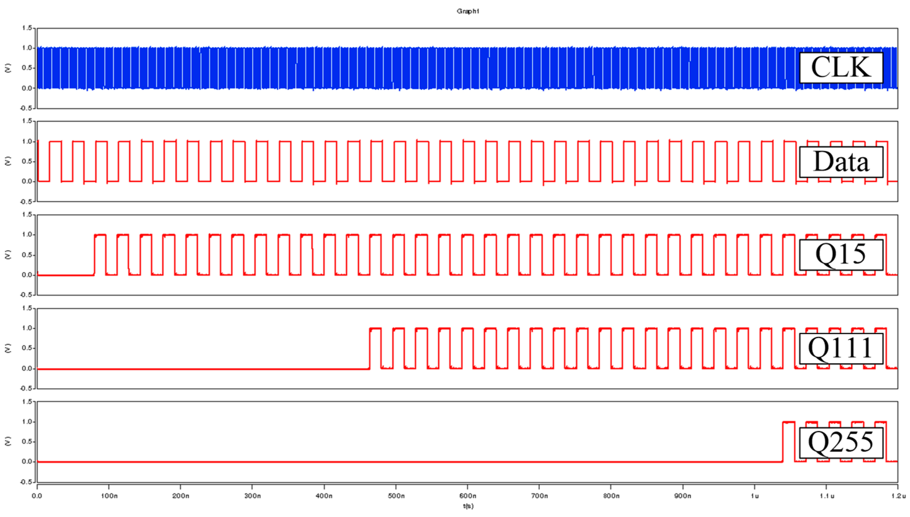
To accomplish the goals of achieving low integrated circuitry layout area and low power consumption, the proposed flip-flop is designed with cross-latch architecture. Since the conventional master–slave (MS) latch transmission gate flip-flop (TGFF) is the most widely used flip-flop, it is necessary to make a comparison between this proposed CLSR scheme and the traditional MS latch flip-flop. The proposed CLSR scheme was implemented in TSMC-40 nm CMOS process standard technology [33]. Figure 7 shows the post-simulation results of the proposed 256-bit CLSR design under the process of 1GHz/TT corner frequency at a supply voltage of 0.9 V. The output QN is generated by shifting the input data according to the clock signal. When the clock is triggered positively 16 times, the data are shifted by 16-bit, and the signal of Q15 is generated. When the clock is triggered positively 256 times, the data are shifted by 256-bit, and the signal of Q255 is generated. It can be seen that after adding a delay clock circuit (Figure 6c), the above-mentioned glitch issue is clearly wiped out.
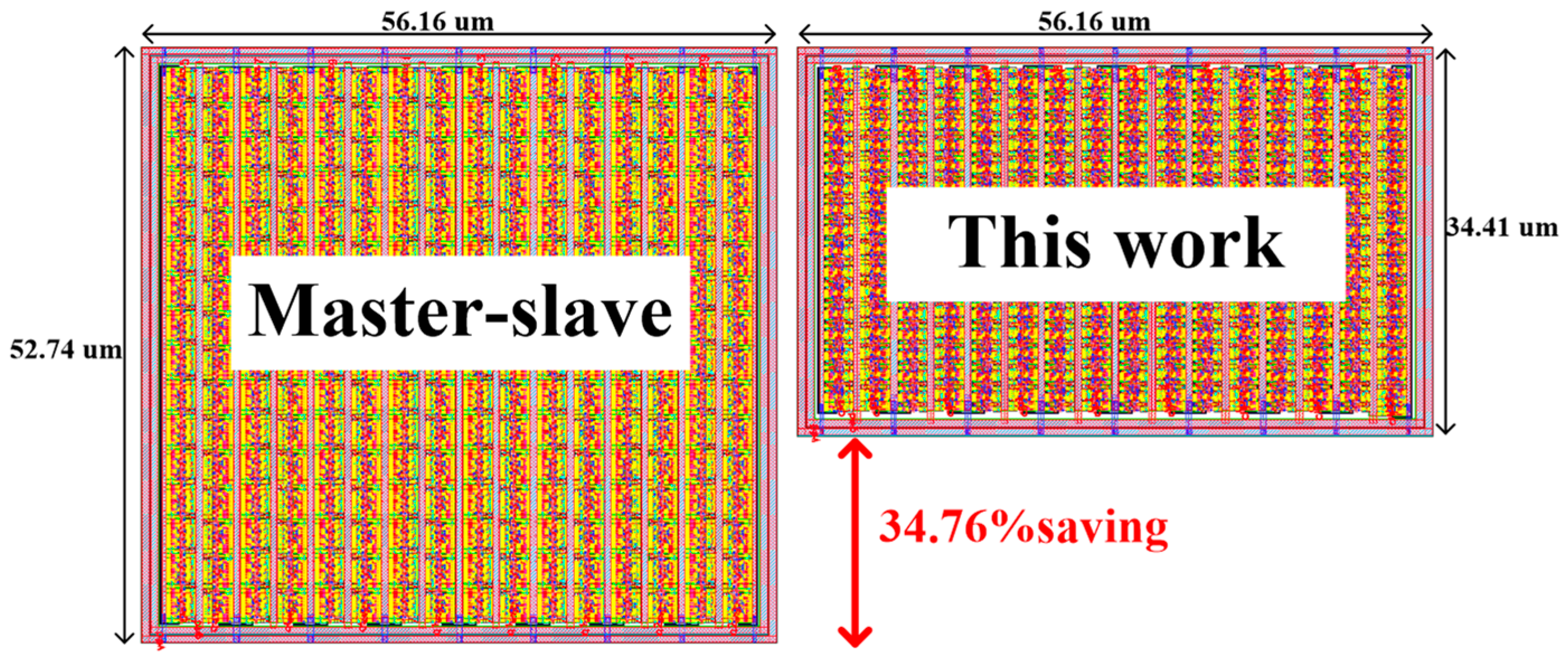
Figure 8 shows the layout comparison between a 256-bit shift register that was constructed based on this proposed CLSR scheme and the conventional master–slave latch architecture. The number of transistors in the conventional MS latches shift register design is 6144, and the number in the proposed CLSR scheme design is 3174. Compared with the conventional MS latches shift register, the number of transistors in the proposed CLSR scheme can be reduced by 48.33%. To show the advantages of the proposed design in terms of average power consumption, we performed simulations for different conditions.
Figure 9a shows the power consumption of the proposed CLSR scheme design in different switching activities (0–100%) at 0.9 V/250 MHz. Because the required number of transistors is decreased dramatically, the proposed CLSR scheme reduces the average power consumption by 36% compared with the conventional MS latch design. Additionally, the gates capacitances are reduced, and the dynamic power dissipation is suppressed as well. Figure 9b shows a comparison of leakage powers under different word lengths between MS latch and CLSR architectures. The leakage current of an MS latch shift register is mainly contributed by the inverters and is proportional to the numbers of inverters. In the proposed CLSR scheme, the number of inverters is reduced significantly. Thus, the proposed 256-bit CLSR scheme design saves 60.53% leakage current as compared with the conventional design.
Figure 9c shows the power consumption at different operating frequencies (1 MHz−1 GHz). From the results, the proposed CLSR scheme achieves an average power saving of 35% as compared with the conventional MS latch design. Figure 9d shows the power consumption of the proposed CLSR scheme design under different voltages. To ensure both designs can operate normally, the operating frequency is set at 25 MHz. From the post-layout simulation results, we find that when the proposed CLSR scheme operates from 0.4 V to 0.9 V, it can save 31% power consumption on average compared with the traditional design. Figure 10 shows its optimal power delay product (PDP) performance. The PDP was employed as a composite performance index in this work. For each supply voltage, the CQ delay was scanned to obtain the best PDP number. Both shift register designs were determined to function properly under process variations. The proposed CLSR scheme works well in any kind of simulation trials. According to the above results, the proposed CLSR scheme applied to the application of shift registers achieved better performance such as area, power, and PDP, compared with that of the master–slave architecture. Moreover, to achieve low power design, recently reported works try to extremely reduce the number of transistors [28,29,30]. However, these flip-flops have floating problems of internal nodes. Thus, the reported flip-flops must be selected carefully for different applications.
Finally, Table 2 shows a detailed performance comparison of different 256-bit shift registers. The area of the proposed CLSR scheme design is 1932.47 µm2. Compared with the conventional MS latch shift register (2961.88 µm2), the proposed CLSR scheme design achieves a 34.76% reduction in the integrated circuitry layout area. Table 2 also records the power consumption, leakage power, and PDP at 0.9 V and 0.4 V. When operating at 0.9 V/250 MHz, the proposed design can save up to 36% power consumption and 16.90% PDP. At the same time, due to the large saving of the number of transistors, the proposed CLSR scheme can effectively suppress leakage power consumption [34].

4. Conclusions

This paper proposed a novel cross-latch shift register (CLSR) scheme attempting to reduce power consumption and to eliminate integrated circuity overhead layout area. By using one cross-latch with delay clocking circuit typology to replace the master and slave latches, we reduced the number of transistors by 48.33% as compared with the conventional MS latch shift register. At the same time, the total gates capacitances were reduced, and the static and dynamic power dissipation were suppressed as well. The proposed CLSR scheme was verified by employing TSMC 40 nm CMOS process standard technology. Experimental comparisons with respect to the conventional MS latch design showed that the proposed CLSR scheme not only works well in reducing average power consumption and leakage power but also presents a better performance in circuitry layout area elimination. The research group suggests that a potential application for this novel CLSR scheme is adopting it for digital circuitry-related design approaches.

Author Contributions

J.-F.L. and M.-Y.T. proposed the idea and method; C.-M.T. performed the simulations and experiments; M.-H.S. and P.-Y.K. analyzed the data; P.-Y.K. reviewed the manuscript. All authors have read and agreed to the published version of the manuscript.

Funding

This research received no external funding.

Data Availability Statement

The data presented in this study are available on request from the corresponding author.

Acknowledgments

This work was supported by the Ministry of Science & Technology, Taiwan under contract No. 109-2221-E-324-028, No. 109-2221-E-224-050 and a grant (Grant No. 109AS-11.3.2-ST-a9) from the Council of Agriculture, ROC. The authors would like to acknowledge for technical support in simulation by Taiwan Semiconductor Research Institute, EDA tool support for IC implementation.

Conflicts of Interest

The authors declare no conflict of interest.

References

  1. Ng, T.N.; Schwartz, D.E.; Lavery, L.L.; Whiting, G.L.; Russo, B.; Krusor, B.; Veres, J.; Bröms, P.; Herlogsson, L.; Alam, N. Scalable printed electronics: An organic decoder addressing ferroelectric non-volatile memory. Sci. Rep. 2012, 2, 585. [Google Scholar] [CrossRef]
  2. Gelinck, G.H.; Huitema, H.E.A.; Van Veenendaal, E.; Cantatore, E.; Schrijnemakers, L.; Van Der Putten, J.B.; Geuns, T.C.; Beenhakkers, M.; Giesbers, J.B.; Huisman, B.-H. Flexible active-matrix displays and shift registers based on solution-processed organic transistors. Nat. Mater. 2004, 3, 106–110. [Google Scholar] [CrossRef] [PubMed]
  3. Hatamian, M.; Agazzi, O.E.; Creigh, J.; Samueli, H.; Castellano, A.J.; Kruse, D.; Madisetti, A.; Yousefi, N.; Bult, K.; Pai, P. Design considerations for gigabit Ethernet 1000Base-T twisted pair transceivers. In Proceedings of the IEEE 1998 Custom Integrated Circuits Conference (Cat. No. 98CH36143), Santa Clara, CA, USA, 14 May 1998; pp. 335–342. [Google Scholar]
  4. Yamasaki, H.; Shibata, T. A real-time image-feature-extraction and vector-generation VLSI employing arrayed-shift-register architecture. IEEE J. Solid-State Circuits 2007, 42, 2046–2053. [Google Scholar] [CrossRef]
  5. Kim, H.-S.; Yang, J.-H.; Park, S.-H.; Ryu, S.-T.; Cho, G.-H. A 10-bit column-driver IC with parasitic-insensitive iterative charge-sharing based capacitor-string interpolation for mobile active-matrix LCDs. IEEE J. Solid-State Circuits 2014, 49, 766–782. [Google Scholar] [CrossRef]
  6. Chiang, S.-H.W.; Kleinfelder, S. Scaling and design of a 16-mega-pixel CMOS image sensor for electron microscopy. In Proceedings of the 2009 IEEE Nuclear Science Symposium Conference Record (NSS/MIC), Orlando, FL, USA, 24 October–1 November 2009; pp. 1249–1256. [Google Scholar]
  7. Xie, Z.; Wu, Z.; Wu, J. Low Voltage Delay Element with Dynamic Biasing Technique for Fully Integrated Cold-Start in Battery-Assistance DC Energy Harvesting Systems. Appl. Sci. 2020, 10, 6993. [Google Scholar] [CrossRef]
  8. Nomura, S.; Tachibana, F.; Fujita, T.; Teh, C.K.; Usui, H.; Yamane, F.; Miyamoto, Y.; Kumtornkittikul, C.; Hara, H.; Yamashita, T.; et al. A 9.7 mW AAC-decoding, 620 mW H.264 720p 60fps decoding, 8-core media processor with embedded forward body-biasing and power-gating circuit in 65 nm CMOS technology. In Proceedings of the IEEE International Solid-State Circuits Conference-Digest of Technical Papers, San Francisco, CA, USA, 3–7 February 2008; pp. 262–612. [Google Scholar]
  9. Stojanovic, V.; Oklobdzija, V.G. Comparative analysis of master-slave latches and flip-flops for high-performance and low-power systems. IEEE J. Solid-State Circuits 1999, 34, 536–548. [Google Scholar] [CrossRef]
  10. Schwartz, D.E.; Ng, T.N. Comparison of static and dynamic printed organic shift registers. IEEE Electron Device Lett. 2013, 34, 271–273. [Google Scholar] [CrossRef]
  11. Lin, J.-F.; Sheu, M.-H.; Hwang, Y.-T.; Wong, C.-S.; Tsai, M.-Y. Low-power 19-transistor true single-phase clocking flip-flop design based on logic structure reduction schemes. IEEE Trans. Very Large Scale Integr. (TVLSI) Syst. 2017, 25, 3033–3044. [Google Scholar] [CrossRef]
  12. Otfinowski, P.; Grybos, P. Low area 4-bit 5MS/s flash-type digitizer for hybrid-pixel detectors—Design study in 180 nm and 40 nm CMOS. Nucl. Instrum. Methods Phys. Res. Sect. A Accel. Spectrom. Detect. Assoc. Equip. 2015, 800, 104–110. [Google Scholar] [CrossRef]
  13. Kawai, N.; Takayama, S.; Masumi, J.; Kikuchi, N.; Itoh, Y.; Ogawa, K.; Ugawa, A.; Suzuki, H.; Tanaka, Y. A fully static topologically-compressed 21-transistor flip-flop with 75% power saving. IEEE J. Solid-State Circuits 2014, 49, 2526–2533. [Google Scholar] [CrossRef]
  14. Ruiz, G.A.; Granda, M. Efficient low-power register array with transposed access mode. Microelectron. J. 2014, 45, 463–467. [Google Scholar] [CrossRef]
  15. Jamshidi, V.; Fazeli, M. Design of ultra-low power current mode logic gates using magnetic cells. Int. J. Electron. Commun. 2018, 83, 270–279. [Google Scholar] [CrossRef]
  16. Taghizadeh, A.; Koozehkanani, Z.D.; Sobhi, J. A new high-speed low-power and low-offset dynamic comparator with a current-mode offset compensation technique. Int. J. Electron. Commun. 2017, 81, 163–170. [Google Scholar] [CrossRef]
  17. Kumar, D.; Kumar, M. Comparative analysis of adiabatic logic challenges for low power CMOS circuit designs. Microprocess. Microsyst. 2018, 60, 107–121. [Google Scholar] [CrossRef]
  18. Murugasami, R.; Ragupathy, U. Design and comparative analysis of D-Flip-flop using conditional pass transistor logic for high-performance with low-power systems. Microprocess. Microsyst. 2019, 68, 92–101. [Google Scholar] [CrossRef]
  19. Hassanli, K.; Sayedi, S.M.; Dehghani, R.; Jalili, A.; Wikner, J.J. A highly sensitive, low-power, and wide dynamic range CMOS digital pixel sensor. Sens. Actuators Phys. 2015, 236, 82–91. [Google Scholar] [CrossRef]
  20. Jeong, T.T. Implementation of low power adder design and analysis based on power reduction technique. Microelectron. J. 2008, 39, 1880–1886. [Google Scholar] [CrossRef]
  21. Piguet, C. Low-power and low-voltage CMOS digital design. Microelectron. Eng. 1997, 39, 179–208. [Google Scholar] [CrossRef]
  22. Sudheer, A.; Ravindran, A. Design and Implementation of Embedded Logic Flip-Flop for Low Power Applications. Procedia Comput. Sci. 2015, 46, 1393–1400. [Google Scholar] [CrossRef] [Green Version]
  23. Mahmoud, M.M.; El-Dib, D.A.; Fahmy, H.A. Low energy pipelined Dual Base (decimal/binary) Multiplier, DBM, design. Microelectron. J. 2017, 65, 11–20. [Google Scholar] [CrossRef]
  24. Tavana, M.K.; Khameneh, S.A.; Goudarzi, M. Dynamically adaptive register file architecture for energy reduction in embedded processors. Microprocess. Microsyst. 2015, 39, 49–63. [Google Scholar] [CrossRef]
  25. Brelsford, K.; López, S.A.P.; Fernandez-Gomez, S. Energy efficient computation: A silicon perspective. Integration 2014, 47, 1–11. [Google Scholar] [CrossRef]
  26. Katreepalli, R.; Haniotakis, T. Power efficient synchronous counter design. Comput. Electr. Eng. 2019, 75, 288–300. [Google Scholar] [CrossRef]
  27. Yang, B.-D. Low-power and area-efficient shift register using pulsed latches. IEEE Trans. Circuits Syst. I Regul. Pap. 2015, 62, 1564–1571. [Google Scholar] [CrossRef]
  28. Teh, C.K.; Fujita, T.; Hara, H.; Hamada, M. A 77% energy-saving 22-transistor single-phase-clocking D-flip-flop with adaptive-coupling configuration in 40 nm CMOS. In Proceedings of the 2011 IEEE International Solid-State Circuits Conference, San Francisco, CA, USA, 20–24 February 2011; pp. 338–340. [Google Scholar]
  29. Stas, F.; Bol, D. A 0.4-V 0.66-fJ/Cycle Retentive True-Single-Phase-Clock 18T Flip-Flop in 28-nm Fully-Depleted SOI CMOS. IEEE Trans. Circuits Syst. I Regul. Pap. 2017, 65, 935–945. [Google Scholar] [CrossRef]
  30. Li, J.; Chang, A.; Kim, T.T.-H. A 0.4-V, 0.138-fJ/Cycle Single-Phase-Clocking Redundant-Transition-Free 24T Flip-Flop with Change-Sensing Scheme in 40-nm CMOS. IEEE J. Solid-State Circuits 2018, 53, 2806–2817. [Google Scholar]
  31. Kim, Y.; Jung, W.; Lee, I.; Dong, Q.; Henry, M.; Sylvester, D.; Blaauw, D. A static contention-free single-phase-clocked 24t flip-flop in 45nm for low-power applications. In Proceedings of the 2014 IEEE International Solid-State Circuits Conference Digest of Technical Papers (ISSCC), San Francisco, CA, USA, 9–13 February 2014; pp. 466–467. [Google Scholar]
  32. Chang, C.H.; Gu, J.M.; Zhang, M. A review of 0.18-/spl mu/m full adder performances for tree structured arithmetic circuits. IEEE Trans. Very Large Scale Integr. (TVLSI) Syst. 2005, 13, 686–695. [Google Scholar] [CrossRef]
  33. TSMC. 40nm CMOS ASIC Process Digest; Taiwan Semiconductor Manufacturing Company: Taipei, Taiwan, 2009. [Google Scholar]
  34. Roy, K.; Mukhopadhyay, S.; Mahmoodi-Meimand, H. Leakage current mechanisms and leakage reduction techniques in deep-submicrometer CMOS circuits. Proc. IEEE 2003, 91, 305–327. [Google Scholar] [CrossRef] [Green Version]
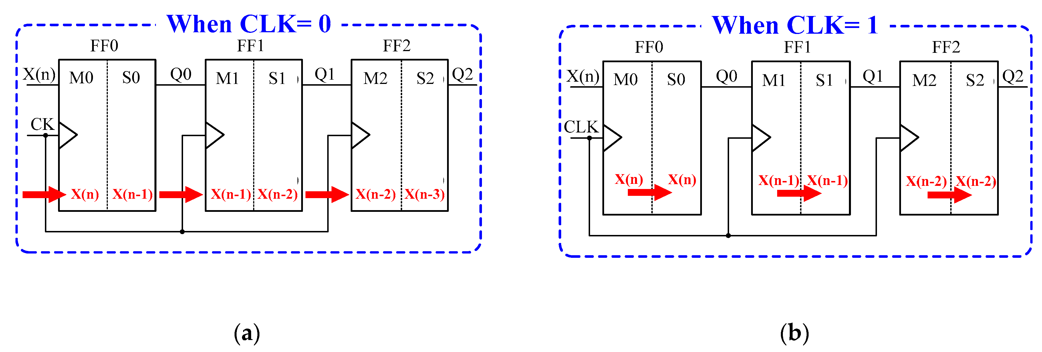
Figure 1. Data transmission of a conventional shift register. (a) When CLK = 0. (b)When CLK = 1.
Applsci 11 00129 g001
Figure 2. Previous master and slave (MS) latches based flip-flop (FF) designs. (a) Transmission gate flip-flop (TGFF). (b) Adaptive coupling flip-flop (ACFF) [28]. (c) True single-phase clock flip-flop (TSPCFF) [29]. (d) Charge sensing flip-flop (CSFF) [30].
Applsci 11 00129 g002
Figure 3. Snapshots of post-layout simulation waveforms. ACFF design: top rows. TSPCFF design: next rows. CSFF design: bottom rows.
Applsci 11 00129 g003
Figure 4. Shift register architectures: (a) master–slave design and (b) the proposed cross-latch shift register (CLSR) design.
Applsci 11 00129 g004
Figure 5. Schematic of the proposed CLSR architecture.
Applsci 11 00129 g005
Figure 6. (a,b) Glitch issue of the proposed CLSR design. (c,d) Proposed delay clock circuit.
Applsci 11 00129 g006
Figure 7. Post layout simulation of 256-bit shift register design based on the proposed CLSR design.
Applsci 11 00129 g007
Figure 8. 256-bit shift register, proposed CLSR scheme and the conventional master–slave latch architecture layout.
Applsci 11 00129 g008
Figure 9. Power consumption performance. (a) Different data switching activity. (b) Leakage power. (c) Different operation frequency. (d) Different supply voltage.
Applsci 11 00129 g009
Figure 10. Power delay product performance at different supply voltages.
Applsci 11 00129 g010
Table 1. Transistor-count comparison of 2-bit latch shift register.
TGFFACFF [28]TSPCFF [29]CSFF [30]CLSR
Number of transistors4844364836
1-bit P/N of transistors12/1211/118/1011/139/9
Floating problemNYYYN
Power (nW)300.10304.00700.70271.10163.90
Area (µm2)16.7615.6713.1618.1813.31
Table 2. Performance comparison of shift registers at TSMC 40 nm.
Master–Slave LatchCLSR
Process40 nm40 nm
Word length of shifter register256256
Number of transistors61443174
Layout area (µm2)2961.881932.47
Typical voltage (V)0.90.40.90.4
Frequency (MHz)2502525025
Power (µW)79426.0950414.24
PDP (fJ)144.43690.22120.03569.61
Leakage power (µW)35.333.3613.952.33
Publisher’s Note: MDPI stays neutral with regard to jurisdictional claims in published maps and institutional affiliations.