Optical and Galvanomagnetic Properties of Bi1-xSbx Thin Films in the Terahertz Frequency Range

 , , , and
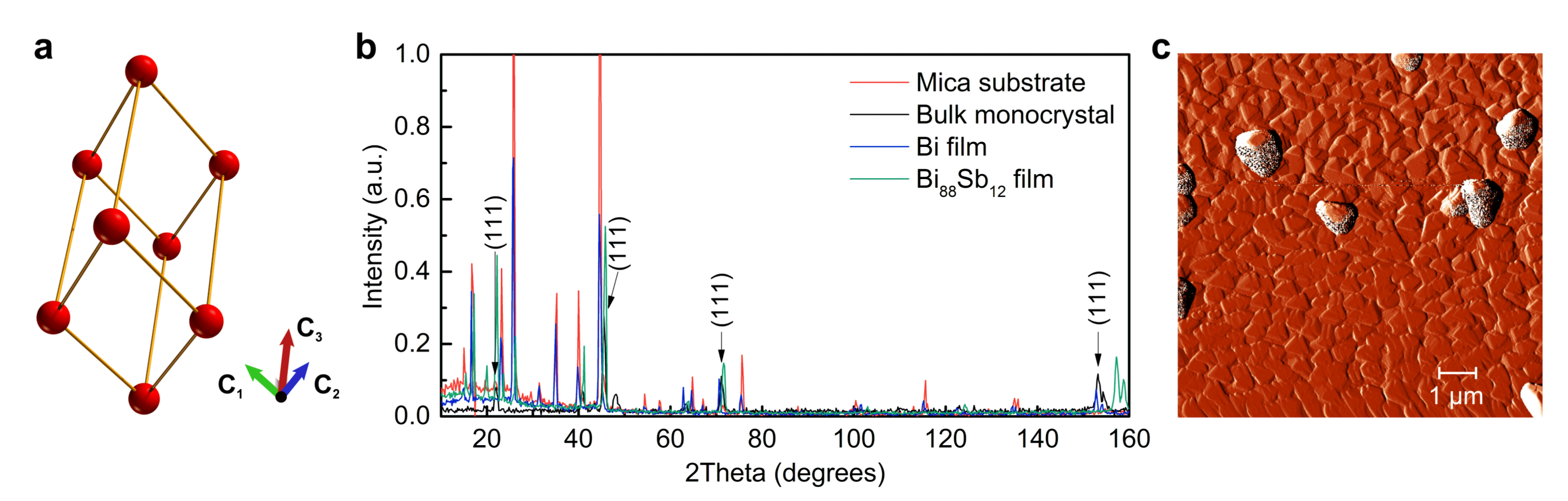
Abstract
1. Introduction
2. Materials and Methods
2.1. Synthesis
2.2. X-ray Diffraction and Atomic Force Microscopy
2.3. Dual-Zone Model of Bismuth-Antimony
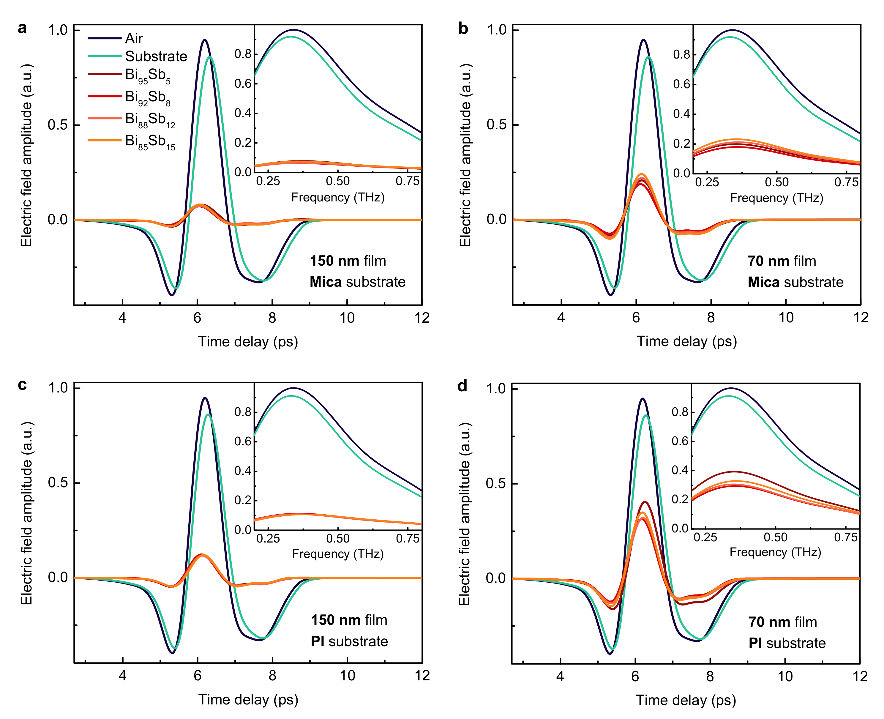
2.4. Terahertz Time-Domain Spectroscopy
3. Results and Discussion
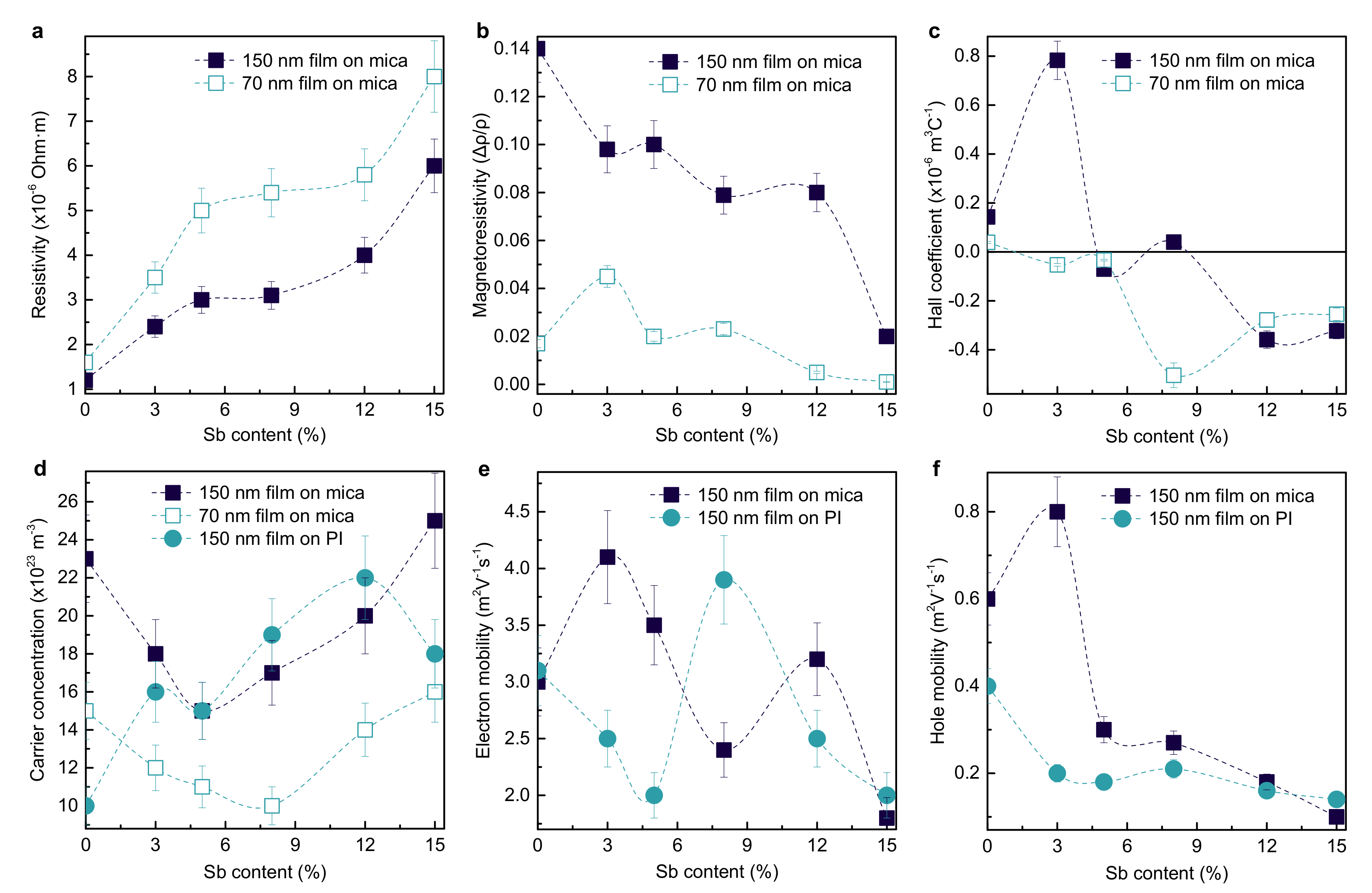
3.1. Resistivity, Magnetoresistivity, and Hall Coefficient
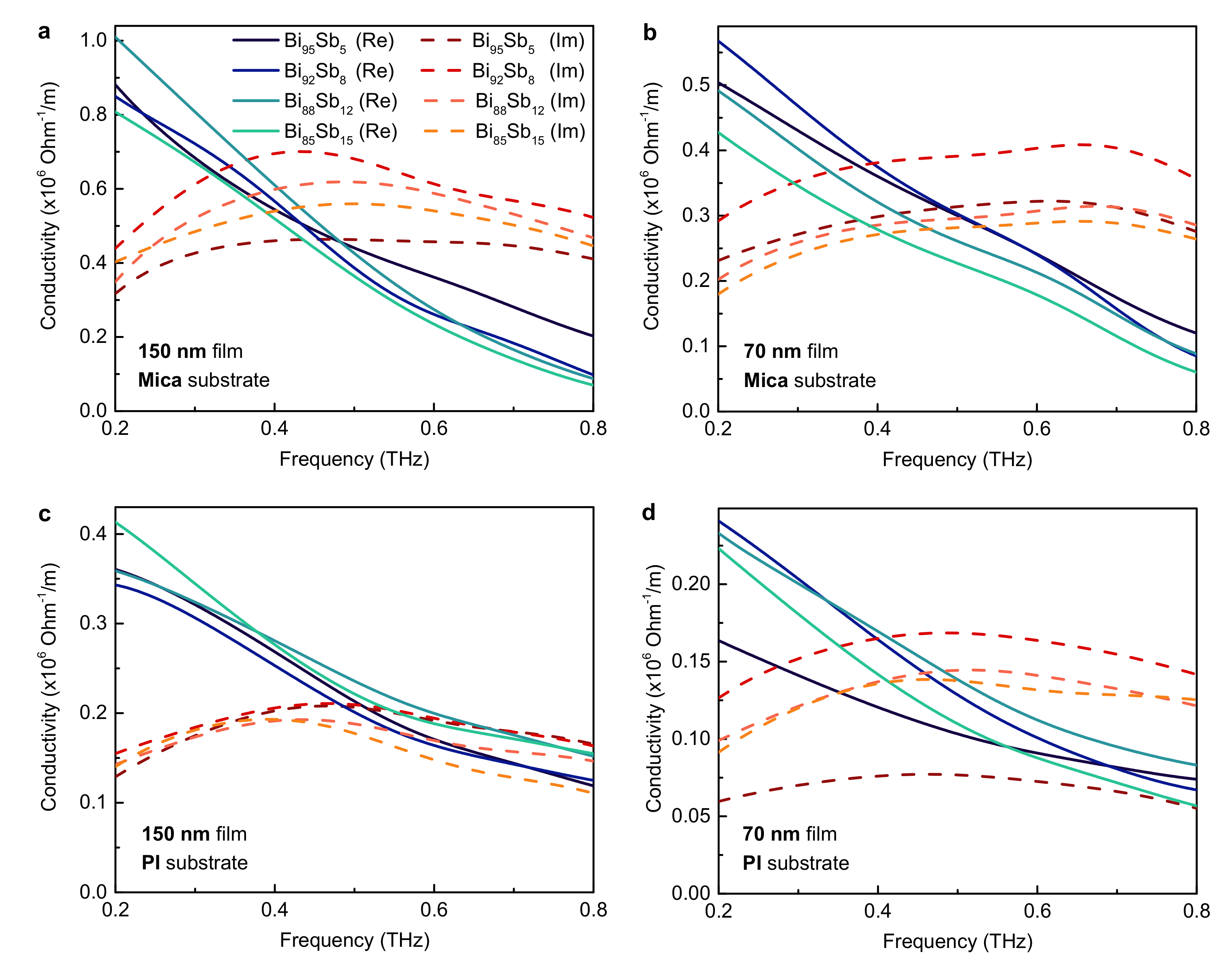
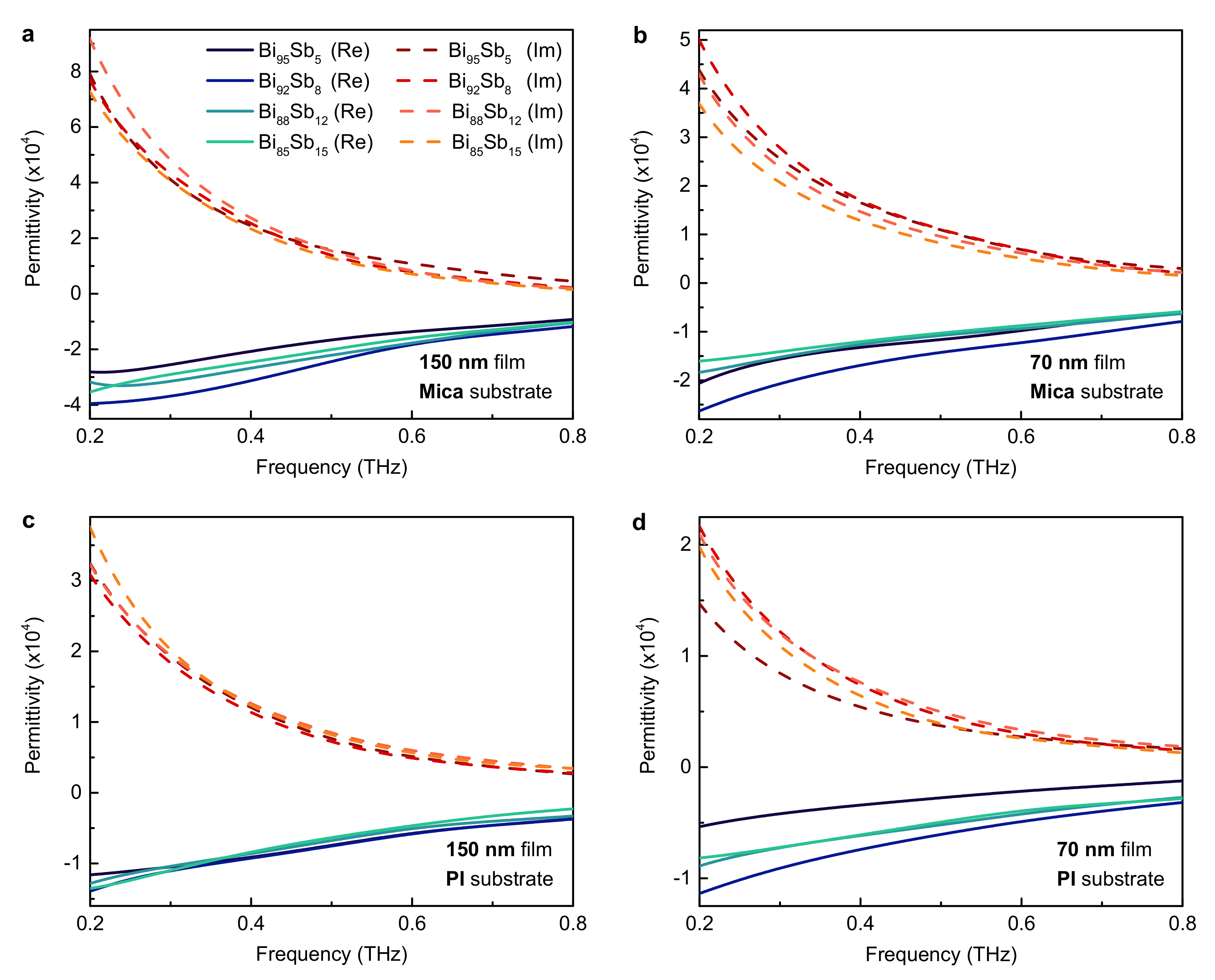
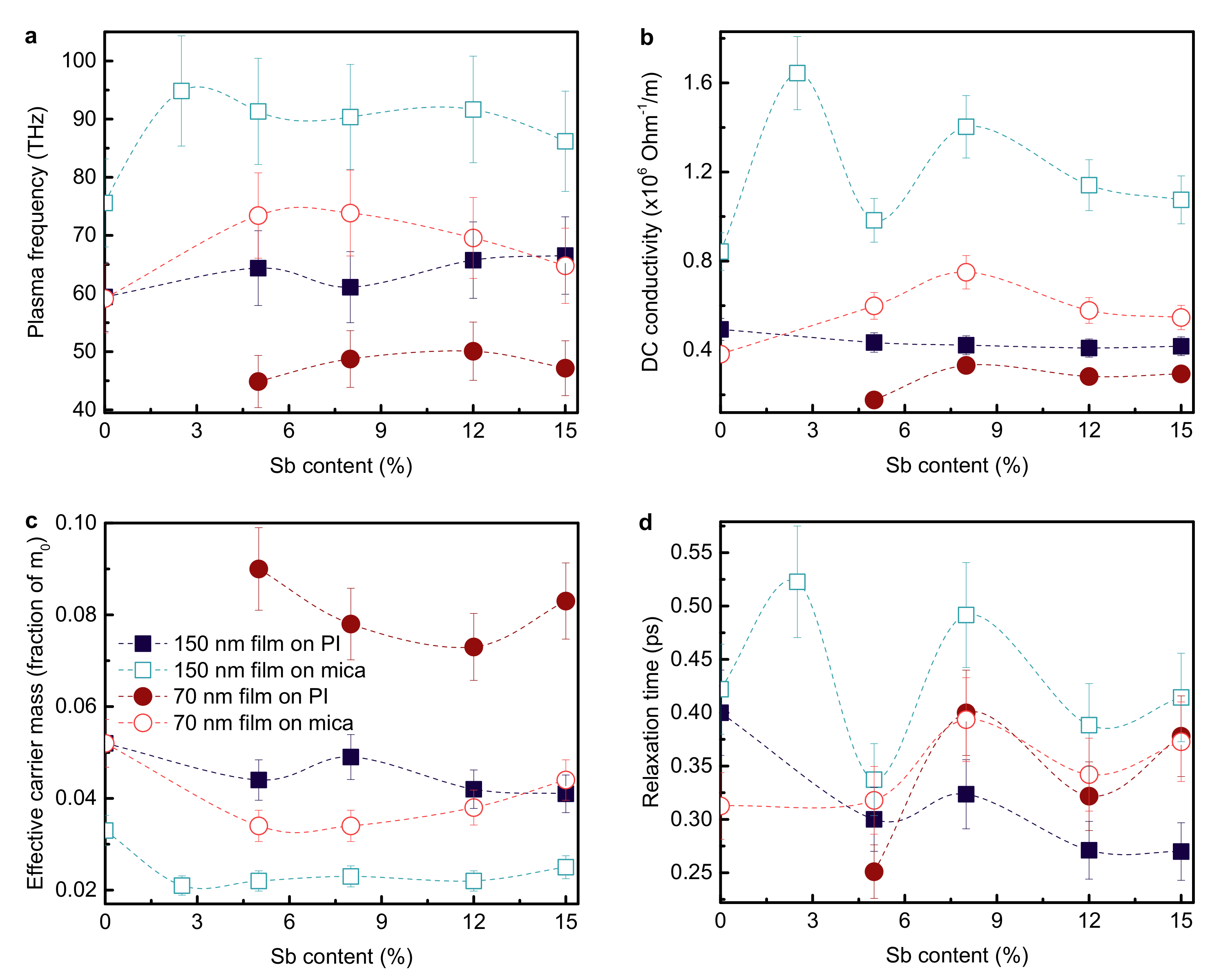
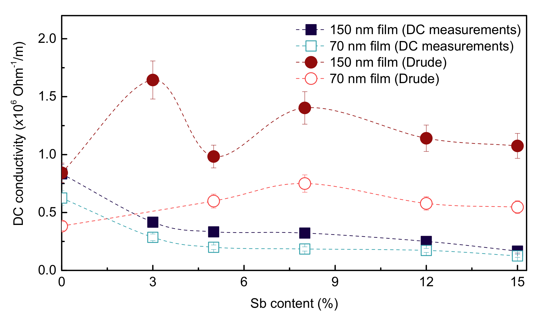
3.2. THz Conductivity and Permittivity
4. Conclusions
Author Contributions
Funding
Conflicts of Interest
References
- Dutta, S.; Shubha, V.; Ramesh, T.; D’sa, F. Thermal and electronic properties of Bi1-xSbx alloys. J. Alloy. Compd. 2009, 467, 305–309. [Google Scholar] [CrossRef]
- Lenoir, B.; Cassart, M.; Michenaud, J.P.; Scherrer, H.; Scherrer, S. Transport properties of Bi-rich Bi-Sb alloys. J. Phys. Chem. Solids 1996, 57, 89–99. [Google Scholar] [CrossRef]
- Cho, S.; DiVenere, A.; Wong, G.K.; Ketterson, J.B.; Meyer, J.R. Transport properties of Bi1-xSbx alloy thin films grown on CdTe (111) B. Phys. Rev. B 1999, 59, 10691. [Google Scholar] [CrossRef]
- Lenoir, B.; Dauscher, A.; Cassart, M.; Ravich, Y.I.; Scherrer, H. Effect of antimony content on the thermoelectric figure of merit of Bi1-xSbx alloys. J. Phys. Chem. Solids 1998, 59, 129–134. [Google Scholar] [CrossRef]
- Malik, K.; Das, D.; Mondal, D.; Chattopadhyay, D.; Deb, A.; Bandyopadhyay, S.; Banerjee, A. Sb concentration dependent structural and resistive properties of polycrystalline Bi-Sb alloys. J. Appl. Phys. 2012, 112, 083706. [Google Scholar] [CrossRef]
- Ohring, M. Materials Science of Thin Films; Elsevier: Amsterdam, The Netherlands, 2001. [Google Scholar]
- Aspnes, D.E. Optical properties of thin films. Thin Solid Films 1982, 89, 249–262. [Google Scholar] [CrossRef]
- Katayama, I.; Kawakami, H.; Hagiwara, T.; Arashida, Y.; Minami, Y.; Nien, L.W.; Handegard, O.; Nagao, T.; Kitajima, M.; Takeda, J. Terahertz-field-induced carrier generation in Bi1-xSbx Dirac electron systems. Phys. Rev. B 2018, 98, 214302. [Google Scholar] [CrossRef]
- Li, X.; Yoshioka, K.; Xie, M.; G Timothy Noe, I.; Lee, W.; Peraca, N.M.; Gao, W.; Hagiwara, T.; Handegård, S.; Nien, L.W.; et al. Terahertz Faraday and Kerr rotation spectroscopy of Bi1-xSbx films in high magnetic fields up to 30 tesla. Phys. Rev. B 2019, 100, 115145. [Google Scholar] [CrossRef]
- Komarov, V.; Suslov, A.; Suslov, M. Galvanomagnetic properties of Bi85Sb15 thin films on different substrates. Semiconductors 2017, 51, 702–705. [Google Scholar] [CrossRef]
- Suslov, A.; Grabov, V.; Komarov, V.; Demidov, E.; Senkevich, S.; Suslov, M. The Band-Structure Parameters of Bi1-xSbx (0≤x≤0.15) Thin Films on Substrates with Different Thermal-Expansion Coefficients. Semiconductors 2019, 53, 611–614. [Google Scholar] [CrossRef]
- Tang, W.; Politano, A.; Guo, C.; Guo, W.; Liu, C.; Wang, L.; Chen, X.; Lu, W. Ultrasensitive Room-Temperature Terahertz Direct Detection Based on a Bismuth Selenide Topological Insulator. Adv. Funct. Mater. 2018, 28, 1801786. [Google Scholar] [CrossRef]
- Wei, Z.; Li, X.; Yin, J.; Huang, R.; Liu, Y.; Wang, W.; Liu, H.; Meng, H.; Liang, R. Active plasmonic band-stop filters based on graphene metamaterial at THz wavelengths. Opt. Express 2016, 24, 14344–14351. [Google Scholar] [CrossRef] [PubMed]
- Grebenchukov, A.N.; Zaitsev, A.D.; Novoselov, M.G.; Kornilov, E.V.; Khodzitsky, M.K. Optically tunable Fano-resonant filter based on graphene. In Metamaterials, Metadevices, and Metasystems 2017; International Society for Optics and Photonics: San Diego, CA, USA, 2017; Volume 10343. [Google Scholar]
- Grebenchukov, A.; Azbite, S.; Zaitsev, A.; Khodzitsky, M. Faraday effect control in graphene-dielectric structure by optical pumping. J. Magn. Magn. Mater. 2019, 472, 25–28. [Google Scholar] [CrossRef]
- Masyukov, M.; Vozianova, A.; Grebenchukov, A.; Gubaidullina, K.; Zaitsev, A.; Khodzitsky, M. Optically tunable terahertz chiral metasurface based on multi-layered graphene. Sci. Rep. 2020, 10, 1–10. [Google Scholar] [CrossRef] [PubMed]
- Onsager, L. Reciprocal Relations in Irreversible Processes. I. Phys. Rev. 1931, 37, 405–426. [Google Scholar] [CrossRef]
- Tinkham, M. Energy gap interpretation of experiments on infrared transmission through superconducting films. Phys. Rev. 1956, 104, 845. [Google Scholar] [CrossRef]
- Novotny, L.; Hecht, B. Principles of Nano-Optics; Cambridge University Press: Cambridge, UK, 2012. [Google Scholar]


© 2020 by the authors. Licensee MDPI, Basel, Switzerland. This article is an open access article distributed under the terms and conditions of the Creative Commons Attribution (CC BY) license (http://creativecommons.org/licenses/by/4.0/).
Share and Cite
Zaitsev, A.D.; Demchenko, P.S.; Zykov, D.V.; Korotina, E.A.; Makarova, E.S.; Tkhorzhevskiy, I.L.; Tukmakova, A.S.; Kablukova, N.S.; Asach, A.V.; Novotelnova, A.V.; et al. Optical and Galvanomagnetic Properties of Bi1-xSbx Thin Films in the Terahertz Frequency Range. Appl. Sci. 2020, 10, 2724. https://doi.org/10.3390/app10082724
Zaitsev AD, Demchenko PS, Zykov DV, Korotina EA, Makarova ES, Tkhorzhevskiy IL, Tukmakova AS, Kablukova NS, Asach AV, Novotelnova AV, et al. Optical and Galvanomagnetic Properties of Bi1-xSbx Thin Films in the Terahertz Frequency Range. Applied Sciences. 2020; 10(8):2724. https://doi.org/10.3390/app10082724
Chicago/Turabian StyleZaitsev, Anton D., Petr S. Demchenko, Dmitry V. Zykov, Ekaterina A. Korotina, Elena S. Makarova, Ivan L. Tkhorzhevskiy, Anastasiia S. Tukmakova, Natallya S. Kablukova, Aleksei V. Asach, Anna V. Novotelnova, and et al. 2020. "Optical and Galvanomagnetic Properties of Bi1-xSbx Thin Films in the Terahertz Frequency Range" Applied Sciences 10, no. 8: 2724. https://doi.org/10.3390/app10082724
APA StyleZaitsev, A. D., Demchenko, P. S., Zykov, D. V., Korotina, E. A., Makarova, E. S., Tkhorzhevskiy, I. L., Tukmakova, A. S., Kablukova, N. S., Asach, A. V., Novotelnova, A. V., & Khodzitsky, M. K. (2020). Optical and Galvanomagnetic Properties of Bi1-xSbx Thin Films in the Terahertz Frequency Range. Applied Sciences, 10(8), 2724. https://doi.org/10.3390/app10082724