Article

Design and Analysis of Heavily Doped n+ Pocket Asymmetrical Junction-Less Double Gate MOSFET for Biomedical Applications

by
Namrata Mendiratta
1,
Suman Lata Tripathi
1,*,
Sanjeevikumar Padmanaban
2,* and
Eklas Hossain
3
1
School of Electronics and Electrical Engineering, Lovely Professional University, Phagwara 144 411, Punjab, India
2
Department of Energy Technology, Aalborg University, Esbjerg 6700, Denmark
3
Department of Electrical Engineering and Renewable Energy, Oregon Tech, Oregon Renewable Energy Center (OREC), Klamath Falls, OR 97601, USA
*
Authors to whom correspondence should be addressed.
Appl. Sci. 2020, 10(7), 2499; https://doi.org/10.3390/app10072499
Submission received: 7 March 2020 / Revised: 28 March 2020 / Accepted: 1 April 2020 / Published: 5 April 2020

Abstract

:
The Complementary Metal-Oxide Semiconductor (CMOS) technology has evolved to a great extent and is being used for different applications like environmental, biomedical, radiofrequency and switching, etc. Metal-Oxide-Semiconductor Field-Effect Transistor (MOSFET) based biosensors are used for detecting various enzymes, molecules, pathogens and antigens efficiently with a less time-consuming process involved in comparison to other options. Early-stage detection of disease is easily possible using Field-Effect Transistor (FET) based biosensors. In this paper, a steep subthreshold heavily doped n+ pocket asymmetrical junctionless MOSFET is designed for biomedical applications by introducing a nanogap cavity region at the gate-oxide interface. The nanogap cavity region is introduced in such a manner that it is sensitive to variation in biomolecules present in the cavity region. The analysis is based on dielectric modulation or changes due to variation in the bio-molecules present in the environment or the human body. The analysis of proposed asymmetrical junctionless MOSFET with nanogap cavity region is carried out with different dielectric materials and variations in cavity length and height inside the gate–oxide interface. Further, this device also showed significant variation for changes in different introduced charged particles or region materials, as simulated through a 2D visual Technology Computer-Aided Design (TCAD) device simulator.

1. Introduction

Detection of various kinds of diseases and molecules like cancer, antigens, viral diseases, and pathogens has been time-consuming and complicated. Using biosensors based on field-effect transistors (FET) for detecting biomolecules like DNA, enzymes, pathogens, cancer, etc. is cost-effective and less time-consuming, and can be used for early-stage detection of diseases [1]. Different biosensors like piezoelectric, nano-mechanic, optical and electrochemical have been made, but they have expensive manufacturing processes and use costly equipment. MOSFET-based biosensors use a simple method of detection without the use of a transducer [2]. Junctionless transistors for detecting biomolecules can be produced by the fabrication industry cheaply in large quantities [3,4,5]. The detection process of biomolecules using FET is based on ISFET (ion-sensitive field effective transistor) which detects charged biomolecules; however, it is unable to detect neutrally charged biomolecules [6,7]. FET-based biosensors work using the electrical properties of the devices (i.e., ON-state current, threshold voltage and capacitances, etc.). In dielectrically modulated FET (DM FET), a cavity is formed in the gate dielectric medium to restrict the movement of charged and non-charged biomolecules for the detection of molecules that are label-free. The biomolecules trapped inside the cavity region change the electrical parameters of the FET [8,9,10,11,12]. Biosensors based on DM FET have some limitations, like Short Channel Effects (SCEs) and problems related to scaling and power supply [13]. To overcome these problems, junctionless MOSFET can be used, which is less prone to SCEs, performs better and has high ON-state current and low OFF-state current. CMOS technology has faced many challenges in the semiconductor industry due to a reduction in the size of the transistor. This has created difficulties in the fabrication of heavily doped ultra-shallow junctions. Further scaling of the device increases the short channel effects (SCEs) [14,15,16,17]. Junction-less transistors were proposed by Colinge to overcome these problems. Junction-less transistors do not require doping and are less susceptible to SCEs. Hence, the fabrication process becomes more comfortable and cheaper. Ajay et al. proposed a double-gate junctionless MOSFET [15] for detecting molecules using the modulation of dielectric material. A nanocavity was introduced in the gate oxide region of the MOSFET using the process of etching from both sides of the device near the drain and source. The molecules trapped in the cavity region bind to the Si O 2 . Furthermore, surface potential in the cavity region is affected [18,19,20]. In this paper, the sensitivity of asymmetrical junctionless double-gate MOSFET (AJ DG MOSFET) with a heavily doped n+ pocket region has been analyzed when subjected to different dielectric oxide materials. Use of different dielectric materials in the cavity created in the gate oxide region has shown significant variation between them, hence making it capable of detecting any small changes in the cavity region. This significant variation in the sensitivity of the device helps detect different biomolecules and can be used for biomedical applications.
The proposed transistor, with a dielectrically modulated cavity region, is formed in the gate oxide region to detect the presence of biomolecules in terms of the variation in dielectric constant. To check the sensitivity of the proposed device toward the biomolecule, the length of the cavity and gate oxide region is varied. Different dielectric materials such as air, SiO 2 ,   HfO 2 and Si 3 N 4 are used to analyze the sensitivity of the device. The device was simulated using the TCAD Cogenda tool. An AJ DG MOSFET with heavily doped n+ pocket region was used as it shows better performance than conventional double-gate junctionless MOSFET (DG JL MOSFET) and asymmetrical junctionless double-gate MOSFET with the absence of an n+ pocket region. The short channel effects like Drain-Induced Barrier Lowering (DIBL) and subthreshold slope are suppressed more in heavily n+ doped pocket AJ DG MOSFET and provide better I ON / I OFF .

2. The Proposed Device Structure

2.1. Proposed Heavily Doped n+ Pocket AJ DG MOSFET

Heavily n+-doped pocket AJ DG MOSFET has two gates arranged in such a way that they are asymmetrical to each other, as shown in Figure 1. A heavily doped n+ pocket region is introduced towards the source side of the MOSFET. The gate contact material used is p+ polysilicon. Hf O 2   is a high-k dielectric material and is used as a gate oxide. Thin-film Si silicon is used as material for the drain, source and channel. The doping concentration of the source region is kept high, equal to that of the n+ pocket region, which improves the ON current of the device. The doping of the drain region is lowered, as that lowers the OFF-state current, therefore providing better   I ON / I OFF . The channel length of the devices varies depending on the ON and OFF state. During the ON state of the MOSFET, the channel length is the length of the overlap region between the two asymmetrical gates, and during its OFF-state, the channel length is the total channel length excluding the length of overlap between the gates. Figure 2 shows the meshing of the device in Visual TCAD, which is based on Genius Device Simulator and is capable of 3D simulation on a colossal scale. The advantages of this simulator are scalability, parallelism and extensibility. Parallel computation used in Genius makes the simulation faster by ten times. The meshing of the channel and oxide is kept tight and should be equal to 1 10 t h of their area, as is shown in Figure 2. The device is simulated in 3D and extended up 1 μm in the z-direction.
Table 1 shows the dimensions of the heavily doped n+ pocket AJ DG MOSFET. The length of the gate ( L gate ) is 20 nm, the length of the overlap region( L overlap ) is 10 nm, the thickness of the silicon ( T silicon ) is 6 nm, the length of the source/drain ( L source = L drain ) is 8 nm, the thickness of the oxide ( T oxide ) is 1 nm, the doping concentration of the pocket region (n+ doping) is 1 × 10 22   cm 3 and the doping concentration of channel region II (n+ doping) is 1 × 10 19   cm 3 . The total channel length( L channel ) , i.e., the length of channel region I plus the length of channel region II, is 30 nm.

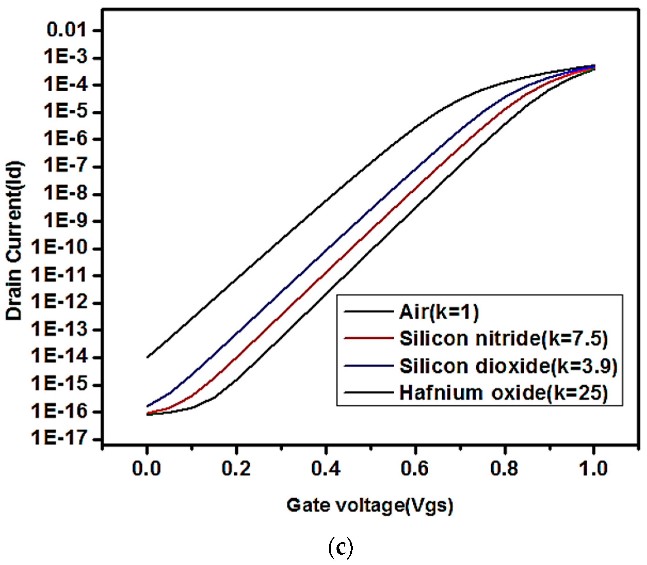
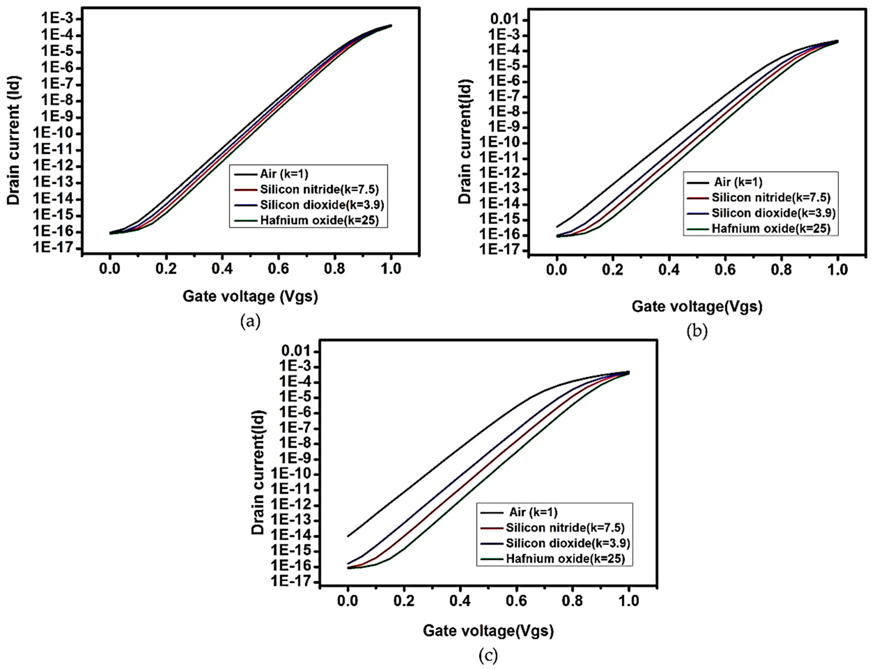
Performance Analysis of Heavily Doped n+ Pocket AJ DG MOSFET

Figure 3 compares the ON and OFF state of the device with and without the n+ pocket region. It is observed that AJ DG MOSFET with an n+ pocket region shows a higher   I ON / I OFF . ratio compared to AJ DG MOSFET without an n+ pocket region. Table 2 represents a comparison of performance parameters between the different device structures.   I ON / I OFF , the ratio of the heavily doped n+ pocket AJ DG MOSFET, is 1013, which is higher than other structures, which indicates that the performance of the proposed device is better. Subthreshold slope (SS) is a short-channel effect which occurs in the subthreshold region due to leakage of current. It is calculated by the formula d V g s d ( l o g I d ) . Drain-Induced Barrier Lowering (DIBL) is also a short-channel effect, which causes a reduction in threshold voltage at higher drain current, and control over the gate is reduced, affecting the performance of the device. It is calculated by the formula V g s V d s . SS and DIBL values for the proposed device are 59 mV/decade and 13.4 mV/V, respectively, which are less than other devices, as shown in Table 2. Therefore, heavily doped n+ pocket AJ DG MOSFET performs better.

2.2. Proposed Heavily Doped n+ Pocket AJ DG MOSFET with a Nanogap-Cavity Region

Figure 4a shows n+ pocket AJ DG MOSFET with a cavity region. A cavity is introduced in the gate oxide region and is filled with the dielectric material. The length (Lcavity) and height (Hcavity) of the nanogap cavity region was varied along with different dielectric materials to analyze the device sensitivity to detect biomolecules. The different dielectric materials selected were air, SiO 2 , HfO 2 and S 3 N 4 . The detection phenomena are based on the electrical parameters like the dielectric constant. The height (Hcavity) of the nanogap cavity taken is 1 nm in Figure 4a. The n+ pocket AJ DG MOSFET with nanogap cavity and thin SiO 2   a   layer is shown in Figure 4b for binding the molecules entering the cavity region, restricting their movements. The height of the cavity region (Hcavity) was 2.7 nm and the thin layer of SiO 2 was 0.3 nm. The device sensitivity for the detection of biomolecules was analyzed by introducing different types of charged particles into the cavity region. The nanogap cavity region can be formed by a thin layer deposition technique followed by a wet etching process. The AJ DG MOSFET with the cavity region works using the dielectric modulation technique for the detection of biomolecules based on the shifting of threshold voltage by variation in dielectric properties. Dielectrically modulated (DM) AJ DG MOSFET is highly sensitive to change in the dielectric constant in the cavity region. However, there are many biomolecules like DNA, enzymes, etc., which contain a charge. The working of the DM AJ DG MOSFET is affected by the presence of charge biomolecules when it enters the nano-gap cavity along with the presence of the constant dielectric effect. Therefore, Figure 4b shows the charge effect of biomolecules along with the effect of the dielectric constant.

3. Investigation Results and Discussion

Figure 5 shows the variation of gate voltage concerning drain current for different dielectric constants with changes in the length of the cavity region. The lengths of the cavity region considered were 3 nm, 5 nm, 7 nm. It was observed that the threshold voltage changed for different dielectric materials. Dielectric materials taken into consideration were air (k = 1),   SiO 2 (k = 3.9), S 3 N 4 . (k = 7.5) and   HfO 2 (k = 25). The threshold voltage for AJ DG MOSFET is shown in Equation (1) [21].
V t h = E g 2 Q + ε S i ε o x t o x t s i + ε S i ε o x 2 t o x Δ Φ 2 + t s i + ε S i ε o x t o x t s i + ε S i ε o x 2 t o x Δ Φ 1
Therefore,
C o x = ε o x t o x = k . ε o t o x
and
Δ Φ 2 = Δ Φ 1
Evaluating Equations (1) and (2):
V t h = E g 2 Q + ε S i t s i C o x + 2   ε S i Δ Φ 2 + t s i C o x + ε S i t s i C o x + 2 ε S i Δ Φ 1
where V t h is the threshold voltage of AJ DG MOSFET, ε S i   is the permittivity of the silicon wafer, ε o x is the permittivity of the gate oxide, Δ Φ is the work function of the gate contact, t s i is the thickness of silicon wafer, t o x is the thickness of gate oxide, ε o is the permittivity of vacuum, and k is the dielectric constant of the material when the cavity region is not introduced in it. When the cavity region in the gate oxide is introduced, the capacitance of the cavity region is also considered. Changing the dielectric material in the cavity region of the MOSFET changes the total capacitance of the gate oxide and the cavity region and hence can be written as
1 C A J   D G   M O S F E T = 1 C o x i d e + 1 C d i e l e c t r i c
1 C A J   D G   M O S F E T = t o x i d e k o x i d e     .     ε 0 + t d i e l e c t r i c k d i e l e c t r i c     .     ε 0
where   C A J   D G   M O S F E T is the total capacitance of the gate oxide along with the cavity region having dielectric material, C d i e l e c t r i c is the capacitance due to dielectric material in the cavity region, t d i e l e c t r i c is the thickness of the dielectric medium, k d i e l e c t r i c   is the dielectric constant in the cavity region, t o x i d e is the thickness of the oxide and k o x i d e   is the dielectric constant of the gate oxide.
From Equations (4)–(6) it can be observed that:
V t h   C d i e l e c t r i c ,   therefore ,   V t h k d i e l e c t r i c    
From Equation (7), it can be seen that the threshold voltage is directly proportional to the constant dielectric present in the cavity region. In Figure 5a–c, the threshold voltage increases with increases in the dielectric constant of the material introduced in the cavity region. Increasing the length of the cavity also shows the variation in threshold voltage, which results in the shifting of channel inversion at a higher threshold voltage. Figure 5a, with the length of the cavity region as 3 nm, shows less variation in the threshold voltage than Figure 5b,c. Therefore, with increases in the dielectric constant, the threshold voltage significantly reduces. Hence, this device is highly sensitive to change in dielectric constant and helps detect biomolecules.
Figure 6a–c shows the graph of gate voltage concerning drain current keeping the dielectric material constant and varying the oxide thickness. The oxide thicknesses considered are 1 nm, 3 nm and 5 nm. The length of the cavity is kept constant at 5 nm. It can be seen that there is a significant variation in threshold voltage with a change in oxide thickness. Changing the oxide thickness also changes the thickness of the cavity region. The effect of variation in oxide thickness is considered for dielectric materials in air, silicon nitride, and silicon dioxide. From Equations (6) and (7) mentioned earlier, a change in oxide thickness is observed concerning the threshold voltage.
Therefore:
V t h   1 t o x i d e
and
t o x i d e   t cavity
Equation (8) shows that the thickness of the cavity region (tcavity) is inversely proportional to the threshold voltage. Therefore, decreases in oxide thickness ( t o x i d e ) will increase the threshold voltage. Figure 6a–c shows the variation in the drain current relative to gate voltage with different oxide material regions (air, silicon nitride, silicon dioxide, etc.) present in the cavity region. The observation indicates that when the gate oxide thickness increases, the threshold voltage decreases in proportion. Additionally, the device is highly sensitive to changes in the thickness of the oxide or the height of the cavity region for different dielectric constants. This shows that the suitability of the proposed device for the detection of variation in biomolecules is mainly due to the variation of the dielectric constant in the cavity region.
Figure 7a,b shows the variation in the threshold voltage when different charge particles are introduced in the cavity region. It can be seen that the concentration of charged particles in the cavity region varies with the threshold voltage, and the changes also occur in OFF-state current. Hence, it can be used in detecting the variation in charged particles (both positive and negative). The changes in the number of particles in the cavity region at a certain level show (from 5 × 10¹⁹ to 1018) a sharp effect in OFF-state leakage as well as in subthreshold slope. These changes can be measured in terms of electrical parameters like OFF-state current and threshold voltage. Hence, the device is capable of detecting biomolecules with different dielectric constants and different charge concentrations.

4. Conclusions

In this paper, the properties of an n+ pocket AJ DG MOSFET were analyzed for low-power improved subthreshold characteristics. The proposed n+ pocket AJ DG MOSFET has shown a very high ION/IOFF current ratio of ~1013 with SS of 59 mv/dec and DIBL of 13.9 mV/VA, which shows the device’s suitability for low power applications. A cavity region is introduced in the gate oxide region, and its sensitivity is analyzed concerning the change in dielectric constant and charge concentration. Biomolecules like DNA, enzymes, etc., have different dielectric constants and charge concentrations. AJ DGMOSFET with an n+ pocket region is highly sensitive to changes in dielectric constants as well as charge concentrations and can be used as a biosensor effectively. The device with Hf O 2   as the dielectric material performs better.
The structure of the device is simple, and the cost of manufacturing is low. Finally, it can be concluded that this device has a low OFF-state current and high I ON / I OFF ratio providing better performance. It is also less prone to short channel effects. Therefore, this device can be used as a biosensor for detecting different types of diseases at early stages.

Author Contributions

N.M., S.L.T., S.P., devised the project, the main conceptual ideas, design experimentation and writing—first draft preparation; S.P., S.L.T., supervision, data validation and review and editing; S.P., E.H., project administration, software; S.P., technical input for testing and validation of results; S.P., S.L.T., E.H., review and suggestion for improvement. All authors have read and agreed to the published version of the manuscript.

Funding

No source of funding for this research activity.

Acknowledgments

Authors would like to thank the Department of Energy Technology, Aalborg University, Esbjerg, Denmark for technical inputs, expertise, transfer knowledge and support.

Conflicts of Interest

The authors declare no conflict of interest.

References

  1. Colinge, J.P.; Lee, C.W.; Afzalian, A.; Akhavan, N.D.; Yan, R.; Ferain, I.; Razavi, P.; Neill, B.O.; Blake, A.; White, M.; et al. Nanowire transistors without junctions. Nat. Nanotechnol. 2010, 5, 225. [Google Scholar] [CrossRef] [PubMed]
  2. Fritz, J.; Baller, M.K.; Lang, H.P.; Rothuizen, H.; Vettiger, P.; Meyer, E.; Guntherodt, H.J.; Gerber, C.; Gimzewski, J.K. Translating biomolecular recognition into nano-mechanics. Science 2000, 288, 316–318. [Google Scholar] [CrossRef] [PubMed] [Green Version]
  3. Maji, M.; Saini, G. Modeling of dual material surrounding split gate junctionless transistor as biosensor. Superlattices Microstruct. 2019, 135, 106–290. [Google Scholar] [CrossRef]
  4. Buvaneswari, B.; Balamurugan, N.B. 2D analytical modeling and simulation of dual material DG MOSFET for biosensing application. Int. J. Electron. Commun. 2019, 99, 193–200. [Google Scholar] [CrossRef]
  5. Chanda, M.; Dey, P.S.; De Sarkar, C.K. Novel charge plasma based dielectric modulated impact ionization MOSFET as a biosensor for label-free detection. Superlattice Microstruct. 2015, 86, 446–455. [Google Scholar] [CrossRef]
  6. Singh, S.; Raj, B.; Vishvakarma, S.K. Analytical modeling of split-gate junction-less transistor for a biosensor application. Sens. Bio Sens. Res. 2018, 18, 31–36. [Google Scholar] [CrossRef]
  7. Narang, N.; Saxena, M.; Gupta, M. Investigation of dielectric modulated (DM) double gate (DG) junctionless MOSFETs for application as a biosensors. Superlattice Microstruct. 2015, 85, 557–572. [Google Scholar]
  8. Ghosh, B.; Akram, M.W. Junctionless tunnel field effect transistor. IEEE Electron Device Lett. 2013, 34, 584–586. [Google Scholar] [CrossRef]
  9. Kumar, M.J.; Reddy, G.V. Analytical model for the threshold voltage of dual material gate (DMG) partially depleted SOI MOSFET and evidence for reduced short-channel effects. Solid State Integr. Circuits Technol. Proc. 7th Int. Conf. IEEE 2004, 2, 1204–1207. [Google Scholar]
  10. Narang, R.; Saxena, M.; Gupta, M. Comparative analysis of dielectric-modulated FET and TFET-based biosensor. IEEE Trans. Nanotechnol. 2015, 143, 427–435. [Google Scholar] [CrossRef]
  11. Narang, R.; Saxena, M.; Gupta, M. Analysis of gate underlap channel double gate MOS transistor for electrical detection of bio-molecules. Superlattice Microstruct. 2015, 88, 225–243. [Google Scholar]
  12. Kim, C.; Ahn, J.; Lee, K.; Jung, C.; Park, H.G.; Choi, Y. A new sensing metric to reduce data fluctuations in a nanogap-embedded field-effect transistor biosensor. IEEE Trans. Electron. Devices 2012, 59, 2825–2831. [Google Scholar] [CrossRef]
  13. Im, H.; Huang, X.J.; Gu, B.; Choi, Y.K. A dielectric-modulated field-effect transistor for biosensing. Nat. Nanotechnol. 2007, 2, 430–434. [Google Scholar] [CrossRef] [PubMed]
  14. Kim, S.; Baek, D.; Kim, J.Y.; Choi, S.J.; Seol, M.L.; Choi, Y.K. A transistor-based biosensor for the extraction of physical properties from biomolecules. Appl. Phys. Lett. 2012, 101, 073703. [Google Scholar] [CrossRef] [Green Version]
  15. Ajay, R.; Narang, M.; Saxena, M. Modeling of gate underlapjunctionless double gate MOSFET as bio-sensor. Mater. Sci. Semicond. Process. 2017, 71, 240–251. [Google Scholar] [CrossRef]
  16. Lee, C.W.; Afzalian, A.; Akhavan, N.D.; Yan, R.; Ferain, I.; Colinge, J.P. Junctionlessmultigate field-effect transistor. Appl. Phys. Lett. 2009, 94, 13–15. [Google Scholar]
  17. Chakraborty, A.; Sarkar, A. Analytical modeling and sensitivity analysis of dielectric-modulated junctionless gate stack surrounding gate MOSFET (JLGSSRG) for application as biosensor. J. Comput. Electron. 2017, 16, 556–567. [Google Scholar] [CrossRef]
  18. Wang, Y.; Tang, Y.; Sun, L.; Cao, F. High performance of junctionlessMOSFETwith asymmetric gate. Superlattices Microstruct. 2016, 97, 8–14. [Google Scholar] [CrossRef]
  19. Yeo, Y.C. Metal gate technology for nanoscale transistors—Material selection and process integration issues. Thin Solid Film. 2004, 462, 34–41. [Google Scholar] [CrossRef]
  20. Kumari, V.; Saxena, M.; Gupta, R.S.; Gupta, M. Two dimensional analytical Drain current model for Double Gate MOSFET incorporating Dielectric Pocket. IEEE Trans. Electron Devices 2012, 59, 2567–2574. [Google Scholar] [CrossRef]
  21. Taur, Y. Analytic Solutions of Charge and Capacitance in Symmetric and Asymmetric Double-Gate MOSFETs. IEEE Trans. Electron Devices 2001, 48, 2861–2869. [Google Scholar] [CrossRef]
Figure 1. Structure of heavily n+-doped pocket AJ DG MOSFET.
Applsci 10 02499 g001
Figure 2. The meshing of the heavily n+-doped pocket AJ DG MOSFET in TCAD.
Applsci 10 02499 g002
Figure 3. Drain current variations concerning gate voltage for heavily doped n+ pocket AJ DG MOSFET.
Applsci 10 02499 g003
Figure 4. (a) n+ pocket AJ DG MOSFET with a cavity region; (b) n+ pocket AJ DG MOSFET with a cavity region over a S i O 2 layer.
Applsci 10 02499 g004
Figure 5. (a) Drain current versus gate voltage with different dielectric constants (Lcavity = 3 nm); (b) Drain current versus gate voltage with different dielectric constants (Lcavity = 5 nm); (c) Drain current versus gate voltage with different dielectric constants (Lcavity = 7 nm).
Applsci 10 02499 g005aApplsci 10 02499 g005b
Figure 6. Drain current versus gate voltage curve, with (a) air (K = 1) as the dielectric material; (b) silicon nitride (K = 7.5) as the dielectric material; (c) silicon dioxide (K = 3.9) as the dielectric material.
Applsci 10 02499 g006
Figure 7. (a) Graph representing drain current versus gate voltage of the proposed n+ pocket AJ DG MOSFET for p+ charge concentration in the cavity region; (b) Graph representing drain current versus gate voltage of the proposed n+ pocket AJ DG MOSFET for n+ charge concentration in the cavity region.
Applsci 10 02499 g007aApplsci 10 02499 g007b
Table 1. Dimensions of the AJ DG MOSFET with n+ pocket region.
RegionDimension
Gate length (Lgate)20 nm
Length of the overlap region (Loverlap)10 nm
The thickness of silicon (TSilicon)6 nm
Length of the pocket region 10 nm
Length of source/drain8 nm
Gate oxide thickness (Toxide, Hf O 2 as Dielectric material)1 nm
Doping Concentration of pocket region1 × 10 22   cm 3
The doping concentration of channel region II1 × 10 19   cm 3
Table 2. Performance comparison of proposed n+ pocket AJ DG MOSFET with available DG MOSFET device structures.
Device Structure I O N
(A/μm)
I O F F
(A/μm)
I O N / I O F F SS = d V g s d ( l o g I d )
(mV/dec)
DIBL = V g s V d s
(mV/V)
Channel Length
(nm)
AJ DG MOSFET, (2016)127 × 10 6   0.001 × 10 9   1.27 × 10 5 686520
DG MOSFET----4.03 × 10 9 63.3479.5820
n+ Pocket AJ DG MOSFET (proposed work)1.88 × 10 4   9.7 × 10 17   ~10135913.420

