1. Introduction
An electrical power system is generally considered as a large network that connects power plants to customers; it consists of electricity generators and electrical power transmission and distribution networks. One of the most important components in electric power systems is insulators for high-voltage power cables. Cross-linked polyethylene (XLPE), which is a form of polyethylene with crosslinks, is widely used as an insulation material because of its excellent advantages, including high resistance against weather, moisture, and temperature, high mechanical strength, and remarkable electrical properties [
1,
2].
All dielectrics, including XLPE, undergo several alterations in their physical or chemical properties as a result of internal or external environmental factors, e.g., mechanical constraints, humidity, temperature, and partial discharges. Aging can lead to the dielectric breakdown of power cables with XLPE insulation and increase the instability of the electric power system [
3,
4,
5,
6]. Therefore, the study of the aging of XLPE is becoming increasingly important. In the macroscopic regime, measurements of space charge, insulation resistance, and temperature have been applied for detecting the characteristics of the aging of XLPE, whereas in the microscopic regime, X-ray diffraction has been typically used to characterize XLPE insulation [
7]. Above all, it is important to study the influence of defects on the aging phenomenon and the degradation of the insulating performance. The partial discharges induced by defects in the XLPE insulation usually reduce insulation performance in the long term and can act as a factor that further impedes the stability and safety of the overall electric power system. Measurements of partial discharges have been used in one important way to detect defects in XLPE insulation [
8].
Recently, terahertz (THz) spectroscopy and imaging techniques have attracted attention as new methods for studying insulation materials, as well as for realizing nondestructive testing and inspection [
9,
10,
11,
12,
13,
14]. In particular, the photon energy of THz waves, e.g., 4.1 meV at 1 THz, corresponds to the energy range of intermolecular interactions, lattice vibration, and molecular motions such as vibration and rotation. This property enables the investigation of aging effects in XLPE using THz time-domain spectroscopy [
15,
16,
17,
18]. More importantly, THz techniques can be applied to detect defects inside XLPE insulation. Defects such as voids and conducting particles in XLPE insulation can lead to strong and inhomogeneous electric fields around the defects, internal discharges such as treeing discharge, and acceleration of the aging process in polymeric insulated power cables, in order. Detecting the defects using an internal nondestructive examination method is thus particularly important. In addition, the advantage of continuous-wave (CW)-THz imaging systems is that they are able to work contactless and target insulators with extremely low electrical conductivity. Therefore, THz technologies can provide testing methods safer than existing methods that need to get the electrodes in contact such as electrical impedance tomography [
19], or cannot be used for detecting defects in power cables such as Eddy-current testing [
20]. Furthermore, the THz imaging system is expected to be an easy and simple testing method, so it does not require any careful attention by experienced technicians, unlike ultrasonic testing [
21]. In this paper, we used a CW THz imaging system as a nondestructive examination tool for detecting void defects inside XLPE insulation.
2. Materials and Methods
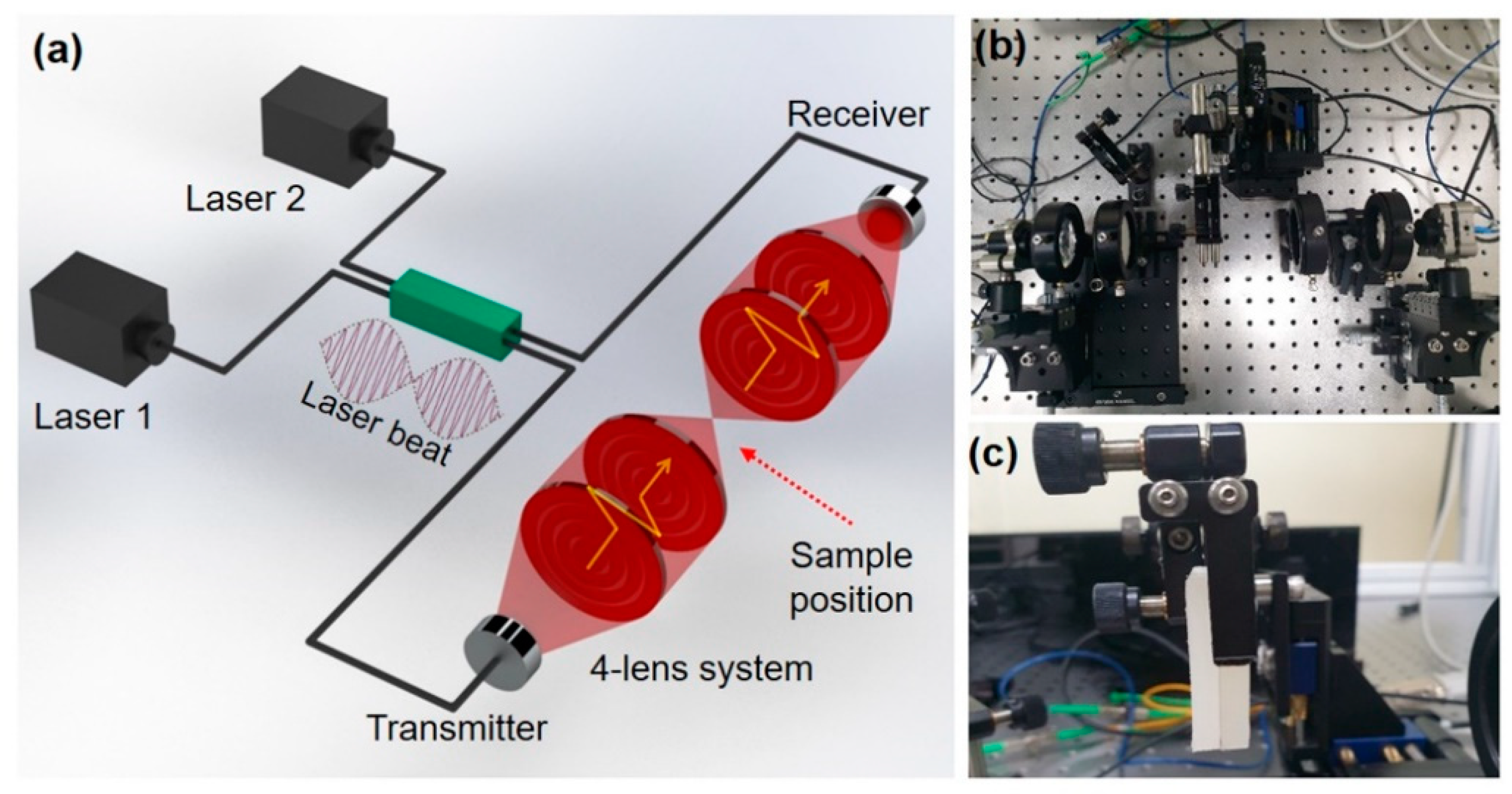
CW–THz radiation was generated by an optical heterodyning method using two distributed feedback (DFB) diode lasers (laser 1 and laser 2 with wavelengths
and
, respectively;
Figure 1a) at 1550 nm. The beat signals, which happen to be the frequency difference,
, between the two lasers, are divided into two parts and illuminate both the transmitter and receiver simultaneously. The photomixer that serves as the THz transmitter is based on an InGaAs/InP semiconductor structure with a bandgap of approximately 1.5
m. When applying a bias voltage to the metal electrodes deposited on the surface of the THz transmitter, the beat signals generate a photocurrent that oscillates at its beat frequency and is then converted into THz radiation.
The generated THz waves are focused at the center of the four-THz-lens system, at which point the samples are placed, as shown in
Figure 1a,b. Both the transmitted THz waves and the beat signals illuminate the photomixer acting as the THz receiver. The beat signals generate photo-carriers, and the amplitude of the electric field of incident THz waves induces the resulting photocurrent. Measurements using the THz receiver, therefore, depend on the phase difference between the beat signal and the incident THz wave. This means that the THz technique shown in
Figure 1 is a coherent detection method that has the advantages of very high efficiency and sensitivity.
In our experiments, the void defects inside the XLPE plates cause a change in the optical path length, compared with the area filled with the XLPE material. The change in phase caused by the difference in optical path length between the defects, and the XLPE material surrounding them corresponds to the change in the amplitude of the measured transmission of the THz waves in the coherent detection scheme. For example, if there is a void defect with 0.3 mm depth in XLPE whose refractive index is around 1.5 at THz frequencies, the difference of optical path lengths between the transmission signals passing through the void defect point and the surrounding material without any void defect is 0.15 mm and the phase difference is π at the frequency of 1 THz. In that case, the direction of photocurrent induced by the THz waves incident on the surface of the THz receive becomes completely reversed and thus the magnitude values of transmitted THz electric field are the same despite that the signs are opposite. Therefore, it is possible to extract a scan image of the samples by measuring the signal size of the transmitted THz waves at each point while moving the XLPE block containing the internal defects along two axes.
To realize an XLPE block sample with artificial void defects inside, we first cut a XLPE plate with a thickness of approximately 10 mm into two pieces of half the total thickness each. On the inner surface of one of the two pieces, artificial void defects of cylindrical shape specifically designed for our experiments were created using a femtosecond laser micromachining method, which is based on laser ablation by amplified femtosecond laser pulses [
22]. Ultrashort laser pulses enable the fabrication of machined structures with high quality, as shown in
Figure 2a, because the duration of laser pulses less than the conduction time of materials reduces the heat effect and minimizes debris. When assembling the two split pieces together, the fabricated void defects were placed inside the XLPE block, as shown in
Figure 1c.
3. Results and Discussion
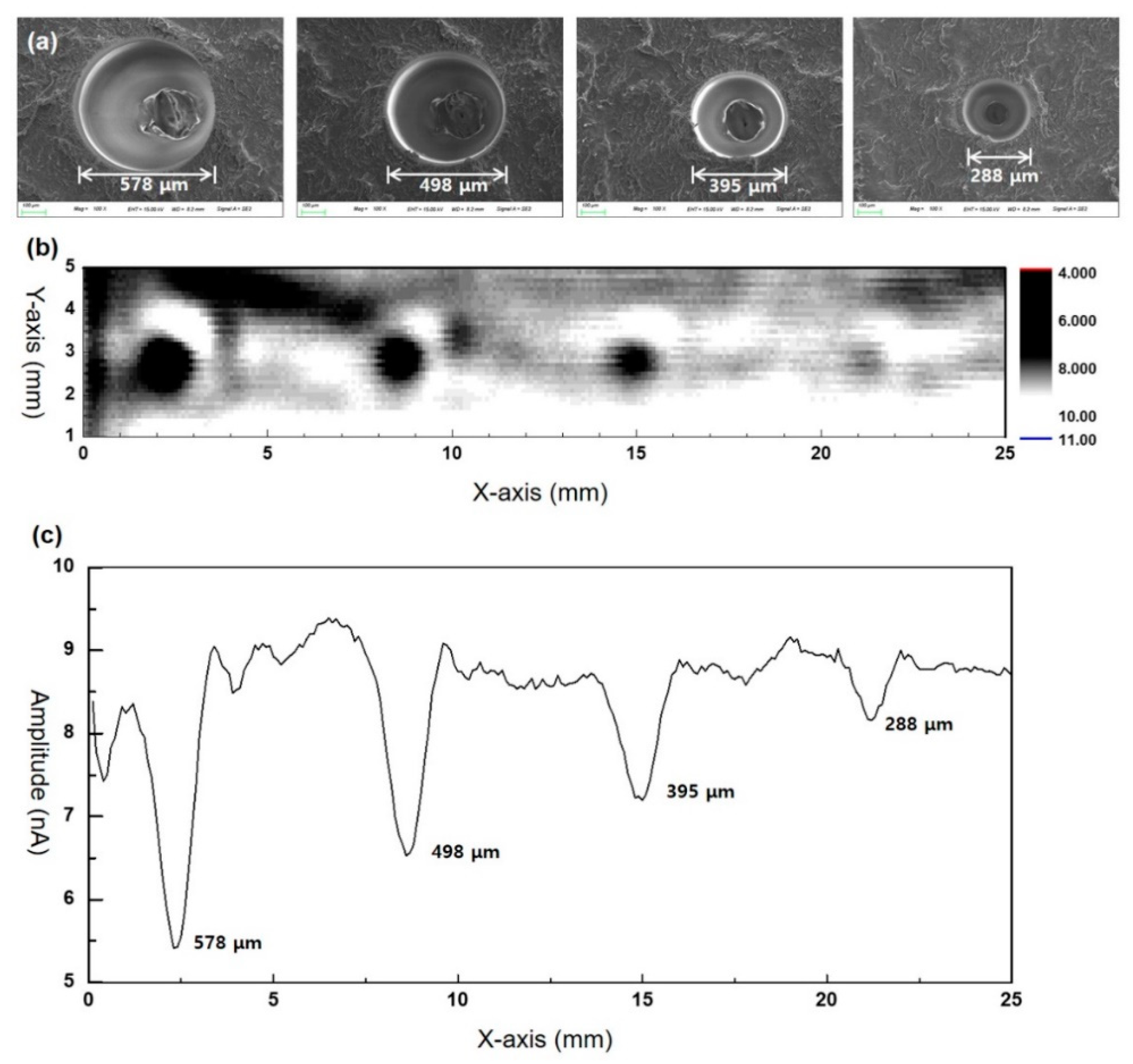
Figure 2a shows scanning electron microscopy images of the artificial void defects fabricated by the laser machining method. For each distance of approximately 6 mm, four side-by-side defects with diameters of 578, 498, 395, and 288 μm, and a depth of 1.2 mm, were formed inside an XLPE plate with a thickness of approximately 10 mm.
Figure 2b shows the two-dimensional amplitude image of the THz waves transmitted through the sample. Because we optimized the transmission signal in the defect-free bulk XLPE plate, the change in the transmitted signal resulting from the void defects appears as dips, as shown by the dark circles in
Figure 2b. The image pinpoints the location of the void defects.
Figure 2c also shows the cross-sectional profile along the
x-axis at the center of the amplitude dips for the four void defects. The results show that not only is identification of a very small defect with a 288-μm diameter possible, but also that extracting information regarding the shape and size of each defect is possible using the CW–THz imaging system.
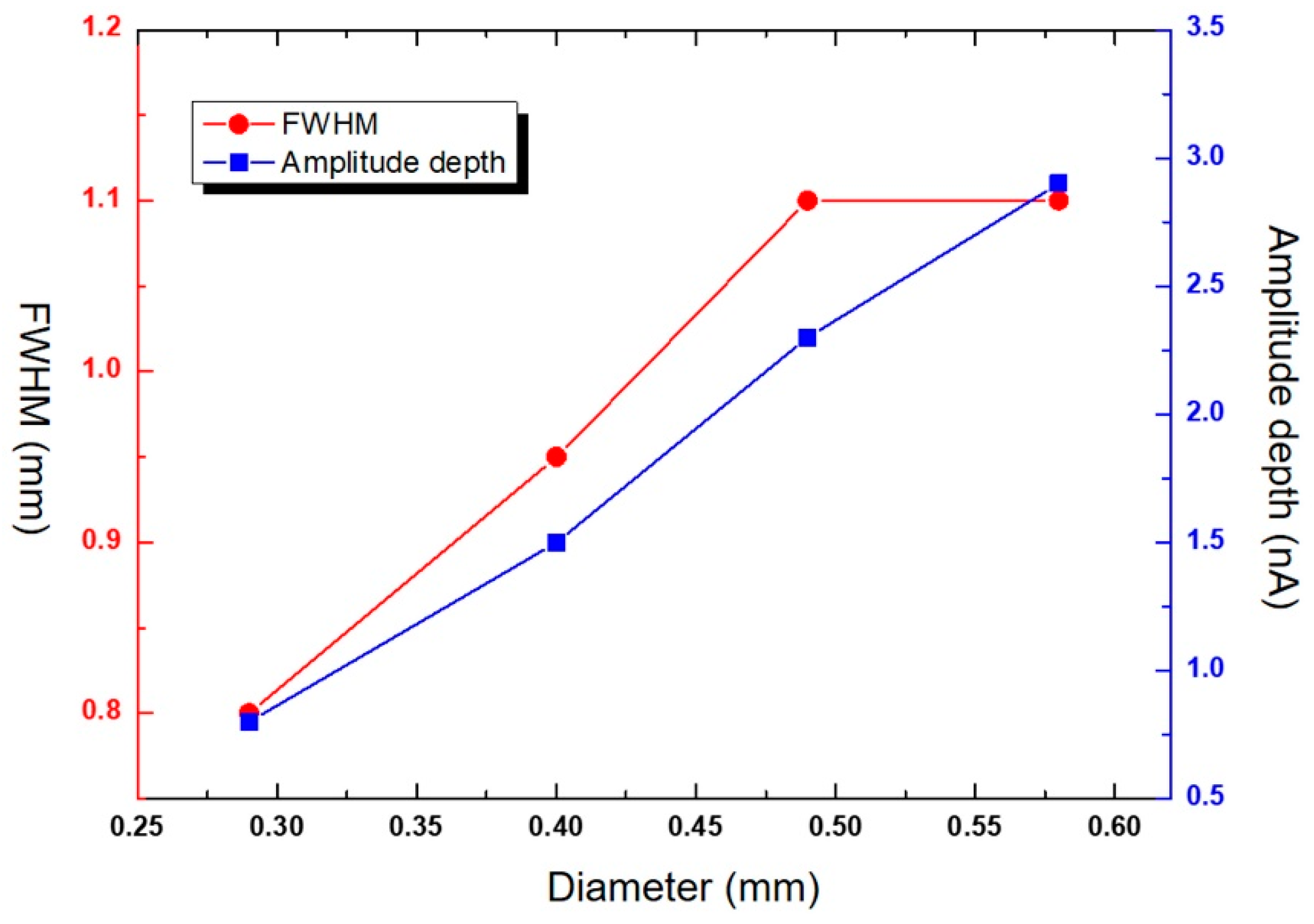
The value of the full width at half maximum (FWHM) and the depth of signal amplitude for four artificial void defects with various diameters, as shown in
Figure 3, show steadily rising curves as the diameter increases. As the diameter of the defect increases, so does the depth of transmission amplitude, and the easier it is to distinguish the defects from the surrounding XLPE material. Even in the smallest defect, with a diameter of 288 μm, the value of amplitude depth, approximately 0.8 nA, is quite distinguishable against the adjacent area, showing a deviation of up to 0.5 nA. The values of FWHM also exhibit a similar trend with respect to the diameter of the defects.
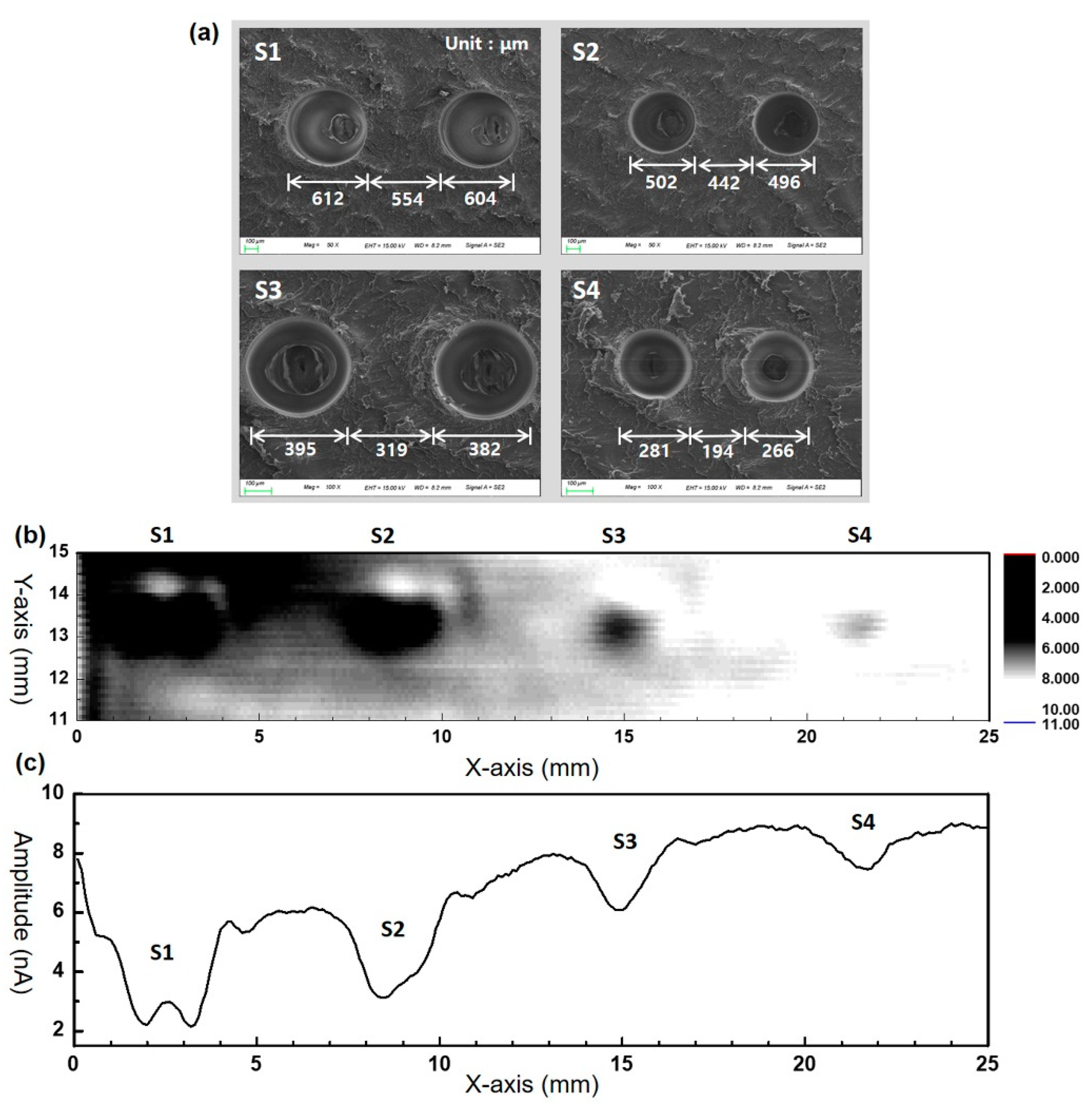
To verify the resolution of the CW–THz imaging system used in the experiment, samples with two adjacent void defects with various diameters and gap widths were produced, as shown in
Figure 4a. The samples were designed to have diameters of 600, 500, 400, and 300 μm and gap widths of 500, 400, 300, and 200 μm, respectively. The actual measured values of the diameter and gap width are shown in
Figure 4a,b, which shows the two-dimensional scanning image of the sample and contains all four structures (denoted S1, S2, S3, and S4). The cross-sectional profile of the transmitted amplitude signal along the
x-axis at the center of the dips more clearly reveals the shape of the artificial void defects, as shown in
Figure 4c.
For the double-void defect with a diameter of approximately 600 μm, S1, the two defects seem to be clearly distinguishable. In addition, in the case of 500 μm, S2, at first glance, it looks like only one dip is observable but there seems to be another small dip on the right shoulder of the main dip. On the contrary, in the case of two structures with diameters of approximately 400 and 300 μm, it is difficult to distinguish the two adjacent void defects. This means that the CW–THz imaging system using a frequency of 1 THz offers a sufficiently distinct resolution up to approximately 500 μm for two adjacent defects.
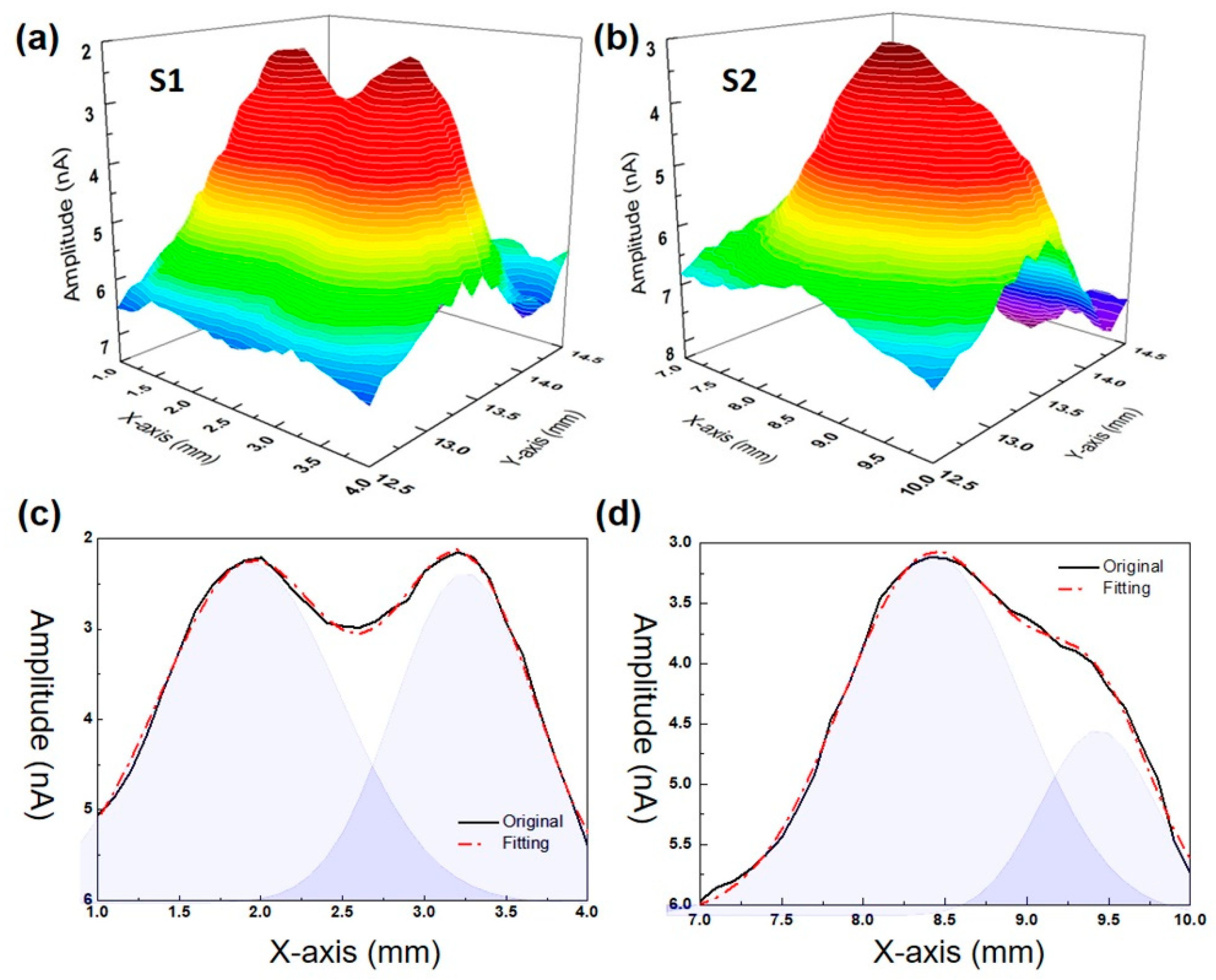
Three-dimensional plots showing the signal amplitude around the double-void defects and the results of double Gaussian fitting of the cross-sectional profiles along the center of defects for S1 and S2 are shown in
Figure 5. For the sake of convenient data analysis, the
y-axis is flipped so that the signals from the defects become peaks. To model the contrast profile of the defect points, we represent the double-void defect signals as the sum of cylindrically symmetric Gaussian peaks, based on the double Gaussian fitting method.
For S1, the center-to-center distance between the two Gaussian peaks is 1.32 μm, which corresponds to the actual value of 1.16 μm obtained from the SEM image. The widths of peaks calculated by the double Gaussian fitting are 1.12 and 0.85 μm. Although the measured values are somewhat larger than the actual sizes, the two adjacent defects are sufficiently distinguishable, not only using the raw image of the transmitted THz amplitude but also by data analysis based on the double Gaussian fitting method.
In contrast, for S2, it is difficult to distinguish the double defects from the raw profiles shown in
Figure 5b,d. The cross-sectional profile along the
x-axis at the center of the amplitude peaks in
Figure 5b was also analyzed using the double Gaussian fitting method. The center-to-center distance and the widths of the peaks extracted by the fitting signals are 1.02, 1.09, and 0.70 μm, respectively. Despite the theoretical difficulty in distinguishing the two defects in S2 because of similar values of the widths of the peaks and the center-to-center distance, the discriminability between two adjacent defects can be increased by employing data analysis and suitable image processing methods.
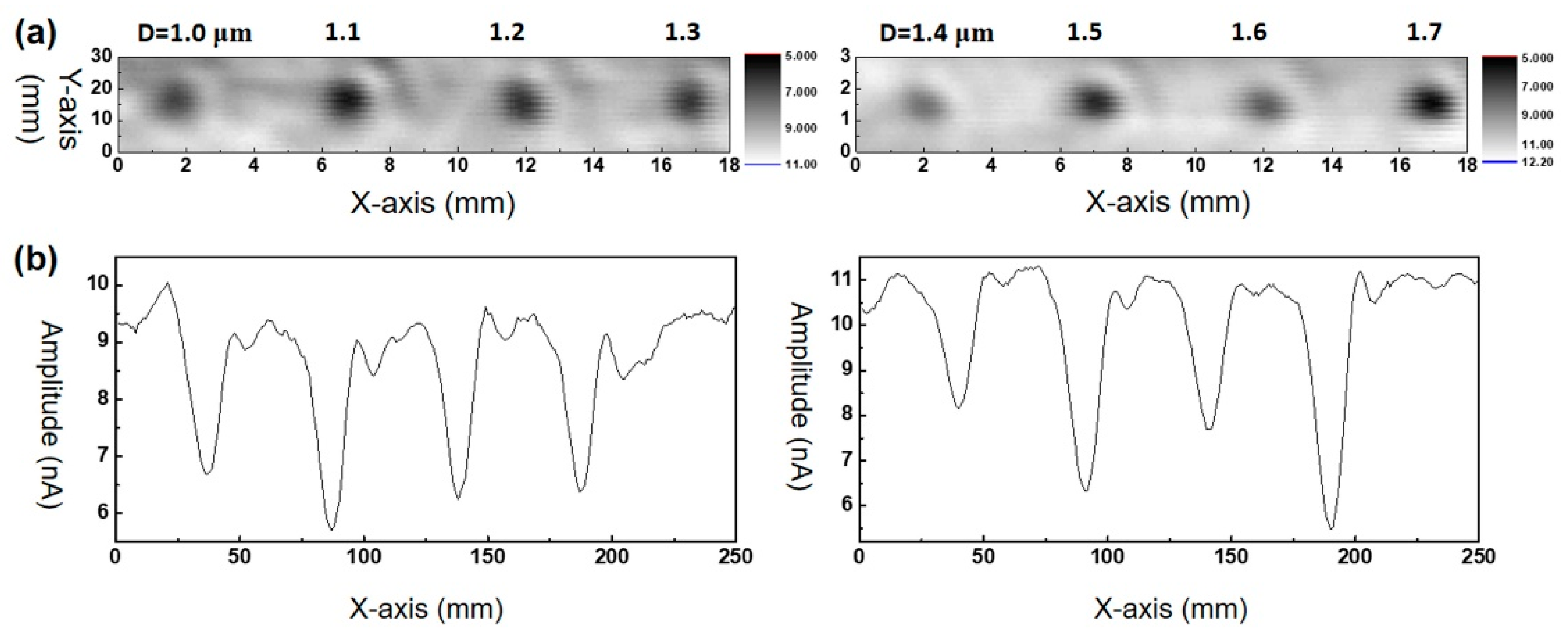
The blind spot problem in the coherent system, finding the difference in thickness of materials by the phase change, occurs when the difference in optical path length from the surroundings matches the wavelength used in the system. The coherent CW–THz system cannot distinguish bulk XLPE without any defect from defects occurring at a phase change of 2π. In that case, the transmitted THz waves can be undetectable. Therefore, to ensure the reliability of the measurements, it is necessary to verify that all defects of varying depths are measurable. We fabricated defects with 1.0 mm diameter and various depths, D, from 1.0 to 1.7 mm with a step size of 100 μm, and measured the samples at a frequency of 1 THz.
Based on the void defects with a refractive index of 1.0 and the XLPE material with a refractive index of approximately 1.5, the optical path difference corresponding to a phase shift of 2π at a frequency of 1 THz will be 600 μm. There is no way to prevent void defects with depths equal to multiples of 600 μm from being blind spots. Otherwise, the results shown in
Figure 6 show that each defect is clearly identified, and only the amplitudes of the dips change slightly depending on D. In addition, the results do not include negative values, which are inevitably predicted to occur near the phase difference of π in the coherent CW–THz imaging system.
The fundamental mechanism of this phenomenon can be assumed to be related to the fact that the width of the beam waist of the CW–THz waves at the focal point is larger than the diameter of the defects. In this case, even if the position of the defects is exactly at the focal point, part of the incident THz waves will pass through the surrounding area instead of the defect area. This effect manifests in the form of signal offsets of the transmission amplitudes. In addition, the THz wave incident on the artificial void defect, which can be classified as a subwavelength, cylindrical dielectric waveguide, experiences a different phase shift at each position. This may eliminate the phenomenon in which the measurement signal is not distinguished because of the blind spots. This means that general types of defects can be readily detected using the coherent CW–THz imaging system.


