Abstract
We demonstrate terahertz single-pixel imaging is improved by using a photomodulator based on silicon passivated with SiO. By exploring various SiO thicknesses, we show that the modulation factor of the as-fabricated terahertz photomodulator can reach 0.9, three times that based on bare silicon. This improvement originates from chemical passivation, as well as anti-reflection. Single-pixel imaging experiments based on the compressed sensing method show that reconstructed images adopting the new photomodulator have better quality than the conventional terahertz modulator based on bare silicon. Since the passivation process is routine and low cost, we expect this work will reduce the cost of terahertz photomodulator and single-pixel THz imaging, and advance their applications.
1. Introduction
Terahertz (THz) imaging has potential applications in a variety of fields, such as non-destructive detection [1,2], security inspection [3,4], and biomedicine [5,6]. Despite great progress, commercially available terahertz focal plane array detectors are still too expensive for most researchers. Therefore, terahertz imaging techniques based on single-pixel detectors have been the focus to date. Among these techniques, computational sampling methods are attractive due to their efficiency compared with the slow mechanical scanning method.
As the key for THz single-pixel imaging based on computational sampling methods, terahertz modulation techniques have received increasing attention. In 2008, Chan et al. [7] adopted standard printed circuit boards as the random matrix to modulate the terahertz transmission, and demonstrated a THz single-pixel imaging by further combining the compressed sensing (CS) algorithm. In order to avoid the use of moving masks, which are difficult to align, Watts et al. [8] made use of a metamaterial spatial modulator, Sensale-Rodriguez et al. [9] employed arrays of graphene electro-absorption modulators, and Kannegulla et al. [10] and Shams et al. [11] demonstrated photo-induced coded-aperture imaging using a semiconductor illuminated by a commercial available digital light processing projector. Recently, silicon wafers have been widely used as THz photomodulators, based on which Stantchev et al. [12,13] demonstrated THz superresolution imaging. She et al. [14] used graphene on silicon as the THz photomodulator and demonstrated THz single-pixel imaging based on the Fourier space spectrum. While various approaches have been adopted to boost photomodulation [15,16,17], there has been less focus on the semiconducting photoconductive materials themselves. Quite recently, Hooper et al. [18] demonstrated that a passivated silicon wafer can greatly improve the efficiency of THz photomodulation. However, THz single-pixel imaging based on such a THz photomodulator has not been reported to date.
In this work, we demonstrate that THz single-pixel imaging based on compressed sensing algorithm can be greatly enhanced by THz photomodulators based on silicon passivated with SiO. We will first show that THz photomodulators based on passivated silicon can have a much higher modulation factor than one based on bare silicon. The effects of the SiO thickness on the photomodulation improvement and the underlying physics will be discussed. Imaging quality based on the as-fabricated THz photomodulators will be compared with the conventional one based on bare silicon.
2. Experimental Setup
Figure 1 illustrates the light-controlled THz modulation and single-pixel imaging system based on a home-built THz time-domain spectroscopy (THz-TDS) system [19]. A pair of biased low-temperature-grown GaAs (LT-GaAs) photoconductive antennas, which are illuminated by femtosecond laser pulses ( nm, <100 fs, 80 MHz; Coherent Vitesse 800-5), are used to generate and detect THz radiations. Collimated THz wave with a diameter of 3.82 mm is directed onto a high-resistance silicon wafer (2000 cm, 500 m thick), both surfaces of which are passivated with SiO. The passivation is realized following a high-temperature thermal oxidation process that is routine in the field of solar cells [20]. The transmitted THz wave is then collected by a single-pixel THz detector. The beam profile (size 4 mm × 4 mm) of an 808 nm linearly polarized (the polarization is parallel to the optical platform) continuous-wave (CW) laser is first patterned by a digital micromirror device (DMD). The DMD, detached from DLP3000 (Texas Instruments), has 608 × 684 micro-mirrors, each of which has a pitch of 7.6 m and behaves as a binary reflector with the maximum frame rate reaching 4000 Hz. The laser beam is then projected onto the passivated silicon. Unless otherwise specified, all the experiments in this work were performed with a high laser power of 330 mW. When the laser spot reflected by the DMD is changed from black to white, the THz transmittance through the passivated silicon decreases from a high level to a low level, i.e., from “1” to “0”. For terahertz single-pixel imaging based on compressed sensing (CS) approach [7,11,21], the target, such as a cartwheel patterned in a gold film, is deposited on top of the front SiO layer.
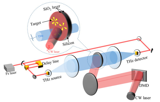
Figure 1.
Schematic of the experimental setup for the THz single-pixel imaging. The CW laser is reflected on the modulator by DMD, and target objects are cartwheels patterned in gold film, which is deposited on the modulator substrate.
For a THz image of pixels to be measured, a series of masks are projected onto the target. The cumulative signal is collected using a single-pixel detector. A series of such measurements with the total number of M lead to [7,21]
where is an vector of measurements, X is the image with pixels ordered in a vector, and denotes the series (with the number of M) of projection masks ordered in an matrix. For each measurement, the projection mask can be generated with Hadamard coding, which consists of “1” and “” elements with each row orthogonal to all other rows [22]. In experiments, the Hadamard projection mask composed of “1” and “” elements is replaced by the substation of two masks and , both of which consist of “1” and “0” elements [12], i.e.,
Therefore, in Equation (1) should be replaced by , where .
Using the CS approach, the number of measurements for assembling the image can be much smaller than the number of image pixels that is . The sampling ratio is defined as
Even with highly undersampled measurement sets, the image can still be accurately reconstructed. In order to reconstruct the THz image, we adopted an algorithm that performs total variation minimization, and that has large signal-to-noise ratio [12,13],
Here is a relaxation variable that determines the smoothness of the reconstructed image, and and are the discretized gradient operators along the horizontal and vertical directions, respectively.
3. THz Photomodulation Experiments
To investigate the effects of the SiO passivation thickness, various thicknesses were prepared. This was achieved by etching the double-sided passivated silicon wafer, where the thickness of each SiO layer was measured to be 287 nm. The passivated silicon wafer was first cut into small pieces of the same size, and was then etched by using 40% potassium hydroxide solution with different duration time. The thickness of the SiO layer was measured by a film thickness meter. Table 1 summarizes the obtained SiO thicknesses of each side (both sides have the same thickness).

Table 1.
As-fabricated silicon wafer with different SiO passivation thicknesses.
The THz time-domain signal transmitted through the sample under CW laser illumination was collected. As a reference, the THz time-domain signal without any modulator was collected. The THz transmittance is then calculated by [23],
where is the frequency of the transmitted THz wave, and are the Fourier transform of and , respectively.
Figure 2a shows that as the SiO thickness increases from 0 nm to 148 nm, the transmittance of the THz field decreases from about 55% to 7%. Further increasing the SiO thickness results in increased transmittance: for the thickness of 287 nm, the transmittance is 30%.
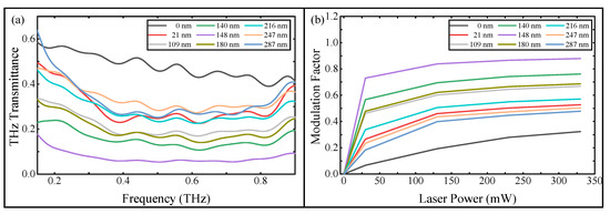
Figure 2.
(a) THz transmittance for different SiO thicknesses. (b) Modulation factor versus CW laser power.
To evaluate the modulation efficiency of different samples, we make use of the modulation factor (MF), which is defined as the change of the integrated transmitted THz power under the illumination [24],
Here, and are the transmitted powers when the laser is off and on, respectively. Figure 2b shows that all the MFs for different SiO thicknesses increase with the CW laser power, where “0 nm” implies the bare silicon wafer. This is because the carrier density in the semiconductor is proportional to the optical power of the laser beam and is modulated through photodoping [25]. Strikingly, for laser power of 330 mW the maximum MF of 0.9 is achieved by sample S5 with SiO thickness of 148 nm; this value is three times of that for the bare silicon ( for sample S1). Figure 3a shows that as the SiO thickness increases, the MFs for different CW laser powers first increase and then decrease, exhibiting maximum values around the SiO thickness of 148 nm.
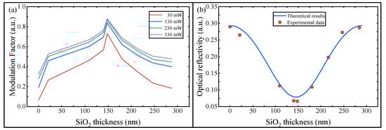
Figure 3.
(a) THz modulation factor versus SiO thickness under the illumination of different CW laser powers. (b) Calculated (blue curve) and measured (red dots) optical reflectivity of the CW laser versus SiO thickness.
To understand the physics origin for the terahertz photomodulation performance, we measured the optical reflectivity of the CW laser by the as-fabricated samples. In experiments, the optical reflectivity was obtained by dividing the power reflected from the sample by that from a gold mirror. Figure 3b shows that as the SiO thickness increases, the optical reflectivity first decreases from about 30% to about 6%, and then increases again to 30%. The smallest optical reflectivity of 6% is achieved for SiO thickness of 147 nm. The experimental data agree well with the theoretical calculation following the Fresnel formulas, where the incidence angle is 25°, and the refractive indices of SiO and silicon at the wavelength of 808 nm are taken to be 1.45 and 3.68, respectively. The optimal thickness of SiO as well as the corresponding minimum optical reflectivity may vary as the incident angle changes. Specifically, for smaller incidence angles, the minimum optical reflectivity can be slightly smaller; for the Brewster angle between the air–SiO interface (), the optical reflectivity of the CW laser keeps at 13% irrespective of the SiO thickness. The independence of the optical reflectivity on the SiO thickness at is due to full transmission through the air–SiO interface in this scenario, thus the optical reflectivity is exactly that by the SiO–Si interface. Although even lower optical reflectivity at small incidence angles can result in even larger MF, in our experiments the specific angle of 25° was used due to space limitation of the experimental setup.
Figure 3 shows that as the SiO thickness increases, the MF of the THz radiation and the optical reflectivity of the CW laser behave reversely. When the SiO thickness increases from 0 nm to the 148 nm, the optical reflectivity decreases, thus the concentration of generated carriers raises and the THz transmittance reduces since more photons impinge onto the silicon wafer producing carriers. When the SiO thickness further increases, the optical reflectivity increases, reducing the photons that can be absorbed by the silicon wafer, the concentration of generated carriers, and the THz transmittance. These suggest the key role played by the anti-reflection effect of SiO2.
However, for samples S1 and S9, both of which have almost the same optical reflectivity, as shown by Figure 3, the former has much smaller terahertz MF than the latter. This is because the dielectric layer added on top of the silicon surface terminates dangling bonds that arise due to the lattice termination, resulting in a reduction in trap density [18]. Therefore, we show that the SiO not only plays a role of chemical passivation, but also acts as an anti-reflection film that enhances the use of light energy [26].
4. THz Single-Pixel Imaging Experiments
We now study the improvement of the THz single-pixel imaging quality by using the as-fabricated THz photo-controlled modulators based on passivated silicon wafers. Three targets were prepared: three-arm, four-arm and six-arm cartwheels.
To quantify the image quality, we adopt signal-to-noise ratio (SNR) as the figure of merit following refs [13,27,28]. It is defined as the average value of intensity in the bright region, , divided by the standard deviation of the noise in the signal-free area of the image, , that is [13,28]
Figure 4 compares the reconstructed terahertz images by using two photomodulators made of the passivated silicon wafer with the highest MF and the conventional bare silicon wafer, i.e., samples S5 and S1. These terahertz images were obtained under the same experimental conditions: the laser power is 330 mW, and the sampling ratio is 100%. Results show that for the bare silicon wafer, the reconstructed images have very poor quality due to the small MF of 0.3, so that the SNR is not available; however, for the passivated silicon wafer with the highest MF of 0.9, the reconstructed image is very clean and clear, and the corresponding SNRs are about 1.0. In other words, the terahertz single-pixel imaging is greatly improved by replacing the conventional photomodulator based on the bare silicon wafer with the new one based on the passivated silicon wafer.
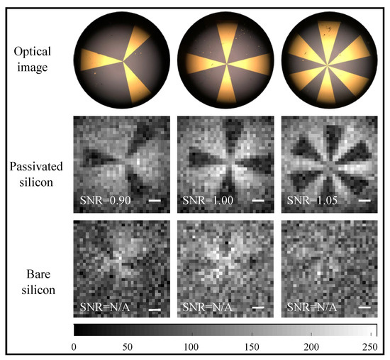
Figure 4.
Top panel: optical images of three targets. Middle and bottom panels: reconstructed terahertz images () based on photomodulators made of passivated and bare silicon wafers, i.e., samples S5 and S0, respectively. The images were reconstructed under full sampling. The scalar bars denote 500 m.
By using the photomodulator made of sample S5, Figure 5 shows that the quality of reconstructed images increases with the sampling ratio in general. The change trend of the SNR with the sampling ratio also confirms this phenomenon, i.e., as the sampling ratio increases, the sharpness of the image gradually increases. The image can be well reconstructed only for sampling ratios of more than 25%. For a sampling ratio of 25%, there still exists pronounced background noise. The noise is greatly suppressed as the sampling ratio increases.
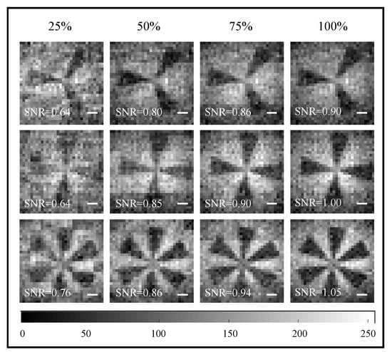
Figure 5.
Reconstructed terahertz images under different sampling ratios: 25%, 50%, 75% and 100%. Scalar bars denote 500 m.
5. Conclusions
In conclusion, we have demonstrated that THz photomodulation and single-pixel imaging is improved by using SiO passivated silicon. By exploring different SiO thicknesses, we have found that for laser illumination power of 330 mW, the largest MF of 0.9 is achieved at a thickness of 148 nm, for which the optical reflectivity reaches the minimum. This MF is three times the MF of bare silicon wafer. We have shown that this great improvement originates from chemical passivation and optical anti-reflection that are both introduced by the SiO passivation. THz single-pixel imaging experiments based on the CS approach have shown that by using the conventional THz photomodulator based on the bare silicon wafer, the reconstructed image had very poor quality; however, by using a greatly improved photomodulator based on the passivated silicon wafer, the reconstructed image is very clean and clear. We have further shown that by using the new photomodulator, sampling ratios above 25% can result in single-pixel THz imaging with acceptable quality. This can greatly reduce the imaging time. Since surface passivation of silicon with SiO is efficient, we expect our work will advance and promote the development of applications of THz photomodulation and single-pixel imaging.
Author Contributions
Conceptualization, R.S., W.L. and Y.L.; methodology, R.S., W.L. and G.W.; software, R.S.; validation, W.L., G.L. and Y.L.; formal analysis, R.S.; investigation, R.S.; resources, Y.L.; data curation, R.S.; writing—original draft preparation, R.S.; writing—review and editing, R.S. and G.L.; visualization, R.S.; supervision, G.L. and Y.L.; project administration, Y.L.; funding acquisition, G.L. and Y.L. All authors have read and agreed to the published version of the manuscript.
Funding
This research was funded by the Shenzhen Research Foundation (Grant Nos. JCYJ20160608153308846, JCYJ20170413152328742, JCYJ20180507182444250), National Key Research and Development Program of China (No. 2017YFC0803506), and Youth Innovation Promotion Association of the Chinese Academy of Sciences (No. 2016320).
Conflicts of Interest
The authors declare no conflict of interest.
References
- Duling, I.; Zimdars, D. Terahertz imaging: Revealing hidden defects. Nat. Photonics 2009, 3, 630. [Google Scholar] [CrossRef]
- Jepsen, P.U.; Cooke, D.G.; Koch, M. Terahertz spectroscopy and imaging—Modern techniques and applications. Laser Photon. Rev. 2011, 5, 124. [Google Scholar] [CrossRef]
- Shen, Y.C.; Lo, T.; Taday, P.F.; Cole, B.E.; Tribe, W.R.; Kemp, M.C. Detection and identification of explosives using terahertz pulsed spectroscopic imaging. Appl. Phys. Lett. 2005, 86, 241116. [Google Scholar] [CrossRef]
- Skvortsov, L.A. Standoff Detection of Hidden Explosives and Cold and Fire Arms by Terahertz Time-Domain Spectroscopy and Active Spectral Imaging (Review). J. Appl. Spectrosc. 2014, 81, 725. [Google Scholar] [CrossRef]
- Zhong, H.; Redo-Sanchez, A.; Zhang, X.C. Identification and classification of chemicals using terahertz reflective spectroscopic focal-plane imaging system. Opt. Express 2006, 14, 9130. [Google Scholar] [CrossRef]
- Shen, Y.C. Terahertz pulsed spectroscopy and imaging for pharmaceutical applications: A review. Int. J. Pharm. 2011, 417, 48. [Google Scholar] [CrossRef]
- Chan, W.L.; Moravec, M.L.; Baraniuk, R.G.; Mittleman, D.M. Terahertz imaging with compressed sensing and phase retrieval. Opt. Lett. 2008, 33, 974. [Google Scholar] [CrossRef]
- Watts, C.M.; Shrekenhamer, D.; Montoya, J.; Lipworth, G.; Hunt, J.; Sleasman, T.; Krishna, S.; Smith, D.R.; Padilla, W.J. Terahertz compressive imaging with metamaterial spatial light modulators. Nat. Photonics 2014, 8, 605. [Google Scholar] [CrossRef]
- Sensale-Rodriguez, B.; Rafique, S.; Yan, R.; Zhu, M.; Protasenko, V.; Jena, D.; Liu, L.; Xing, H.G. Terahertz imaging employing graphene modulator arrays. Opt. Express 2013, 21, 2324. [Google Scholar] [CrossRef]
- Kannegulla, A.; Jiang, Z.; Rahman, S.M.; Shams, M.I.B.; Fay, P.; Xing, H.G.; Cheng, L.J.; Liu, L. Coded-Aperture Imaging Using Photo-Induced Reconfigurable Aperture Arrays for Mapping Terahertz Beams. IEEE Trans. Terahertz Sci. Technol. 2014, 4, 321. [Google Scholar] [CrossRef]
- Shams, M.I.B.; Jiang, Z.; Rahman, S.; Qayyum, J.; Cheng, L.J.; Xing, H.G.; Fay, P.; Liu, L. Approaching real-time terahertz imaging with photo-induced coded apertures and compressed sensing. Electron. Lett. 2014, 50, 801. [Google Scholar] [CrossRef]
- Stantchev, R.I.; Sun, B.; Hornett, S.M.; Hobson, P.A.; Gibson, G.M.; Padgett, M.J.; Hendry, E. Noninvasive, near-field terahertz imaging of hidden objects using a single-pixel detector. Sci. Adv. 2016, 2, e1600190. [Google Scholar] [CrossRef]
- Stantchev, R.I.; Phillips, D.B.; Hobson, P.; Hornett, S.M.; Padgett, M.J.; Hendry, E. Compressed sensing with near-field THz radiation. Optica 2017, 4, 989. [Google Scholar] [CrossRef]
- She, R.; Wenquan, L.; Lu, Y.; Zhou, Z.; Li, G. Fourier single-pixel imaging in the terahertz regime. Appl. Phys. Lett. 2019, 115, 021101. [Google Scholar] [CrossRef]
- Weis, P.; Garcia-Pomar, J.L.; Höh, M.; Reinhard, B.; Brodyanski, A.; Rahm, M. Spectrally Wide-Band Terahertz Wave Modulator Based on Optically Tuned Graphene. ACS Nano 2012, 6, 9118. [Google Scholar] [CrossRef]
- Cao, Y.; Gan, S.; Geng, Z.; Liu, J.; Yang, Y.; Bao, Q.; Chen, H. Optically tuned terahertz modulator based on annealed multilayer MoS2. Sci. Rep. 2016, 6, 22899. [Google Scholar] [CrossRef]
- Yang, D.S.; Jiang, T.; Cheng, X.A. Optically controlled terahertz modulator by liquid-exfoliated multilayer WS2 nanosheets. Opt. Express 2017, 25, 16364. [Google Scholar] [CrossRef]
- Hooper, I.R.; Grant, N.E.; Barr, L.E.; Hornett, S.M.; Murphy, J.D.; Hendry, E. High efficiency photomodulators for millimeter wave and THz radiation. Sci. Rep. 2019, 9, 18304. [Google Scholar] [CrossRef]
- Liu, W.Q.; Lu, Y.F.; Jiao, G.H.; Chen, X.F.; Li, J.Y.; Chen, S.H.; Dong, Y.M.; Lv, J.C. Terahertz optical properties of the cornea. Opt. Commun. 2016, 359, 344. [Google Scholar] [CrossRef]
- Zhao, J.; Wang, A.; Green, M.A. 24.5% Efficiency Silicon PERT Cells on MCZ Substrates and 24.7% Efficiency PERL Cells on FZ Substrates. Prog. Photovolt Res. Appl. 1999, 7, 471. [Google Scholar] [CrossRef]
- Chan, W.L.; Charan, K.; Takhar, D.; Kelly, K.F.; Baraniuk, R.G.; Mittleman, D.M. A single-pixel terahertz imaging system based on compressed sensing. Appl. Phys. Lett. 2008, 93, 121105. [Google Scholar] [CrossRef]
- Valova, I.; Kosugi, Y. Hadamard-based image decomposition and compression. IEEE Trans. Inf. Technol. Biomed. 2000, 4, 306. [Google Scholar] [CrossRef] [PubMed]
- Neu, J.; Schmuttenmaer, C.A. Tutorial: An introduction to terahertz time domain spectroscopy (THz-TDS). J. Appl. Phys. 2018, 124, 231101. [Google Scholar] [CrossRef]
- Wang, G.; Zhang, B.; Ji, H.; Liu, X.; He, T.; Lv, L.; Hou, Y.; Shen, J. Monolayer graphene based organic optical terahertz modulator. Appl. Phys. Lett. 2017, 110, 023301. [Google Scholar] [CrossRef]
- Shrekenhamer, D.; Watts, C.M.; Padilla, W.J. Terahertz single pixel imaging with an optically controlled dynamic spatial light modulator. Opt. Express 2013, 21, 012507. [Google Scholar] [CrossRef]
- Blakers, A.W.; Wang, A.; Milne, A.M.; Zhao, J.; Green, M.A. 22.8% efficient silicon solar cell. Appl. Phys. Lett. 1989, 55, 1363. [Google Scholar] [CrossRef]
- Chen, S.C.; Du, L.H.; Meng, K.; Li, J.; Zhai, Z.H.; Shi, Q.W.; Li, Z.R.; Zhu, L.G. Terahertz wave near-field compressive imaging with a spatial resolution of over λ/100. Opt. Lett. 2019, 44, 21. [Google Scholar] [CrossRef]
- Shchelokova, A.V.; Slobozhanyuk, A.P.; Melchakova, I.V.; Glybovski, S.B.; Webb, A.G.; Kivshar, Y.S.; Belov, P.A. Locally Enhanced Image Quality with Tunable Hybrid Metasurfaces. Phys. Rev. Appl. 2018, 9, 014020. [Google Scholar] [CrossRef]
© 2020 by the authors. Licensee MDPI, Basel, Switzerland. This article is an open access article distributed under the terms and conditions of the Creative Commons Attribution (CC BY) license (http://creativecommons.org/licenses/by/4.0/).