A Differential Measurement System for Surface Topography Based on a Modular Design


Abstract
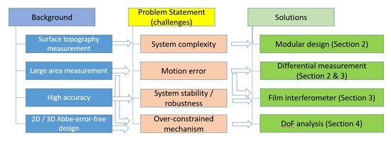
1. Introduction
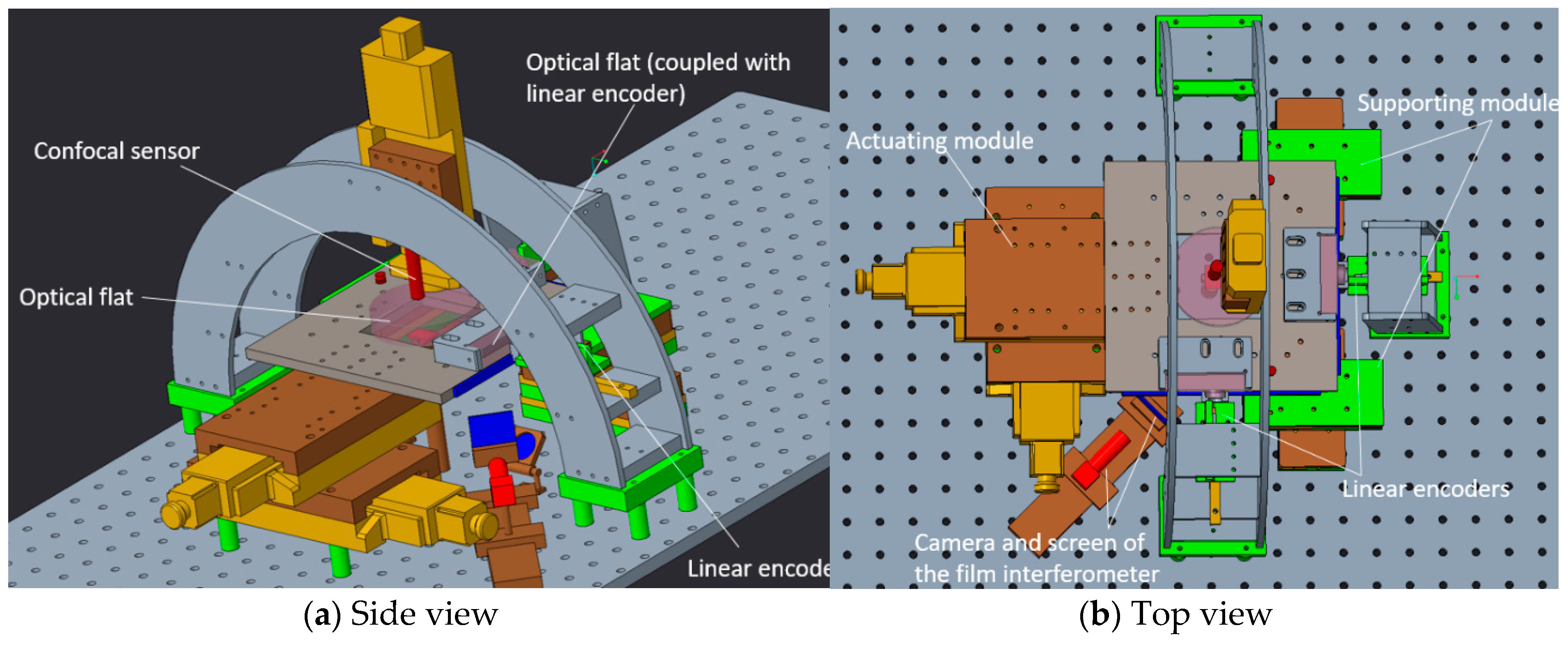
2. Overall System Design
- (1)
- An actuating module, which consisted of two motorized stages.
- (2)
- Supporting modules, each of which consisted of pre-assembled 2D sliders
- (3)
- A differential height measurement module, which consisted of a confocal sensor and a film interferometer
- (4)
- A displacement measurement module, which consisted of an optical gratings couple with the central stage through optical flats.
- (5)
- A datum module, which consisted of three optical flats.
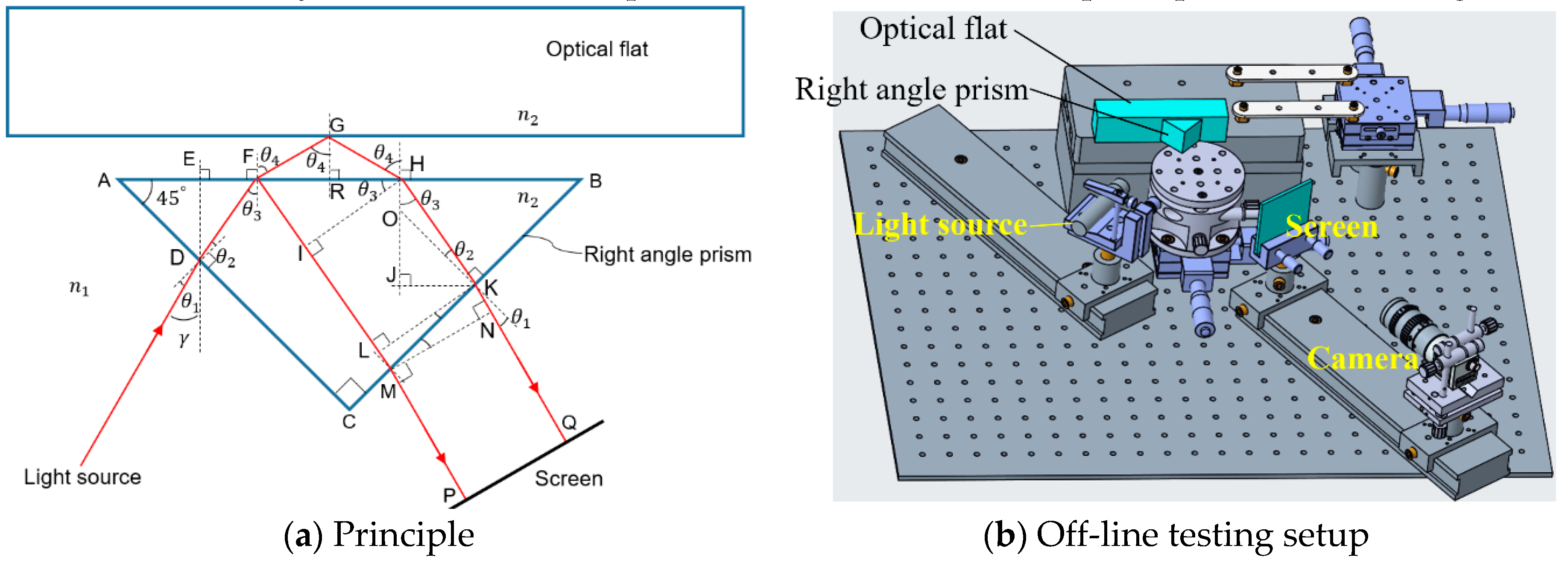
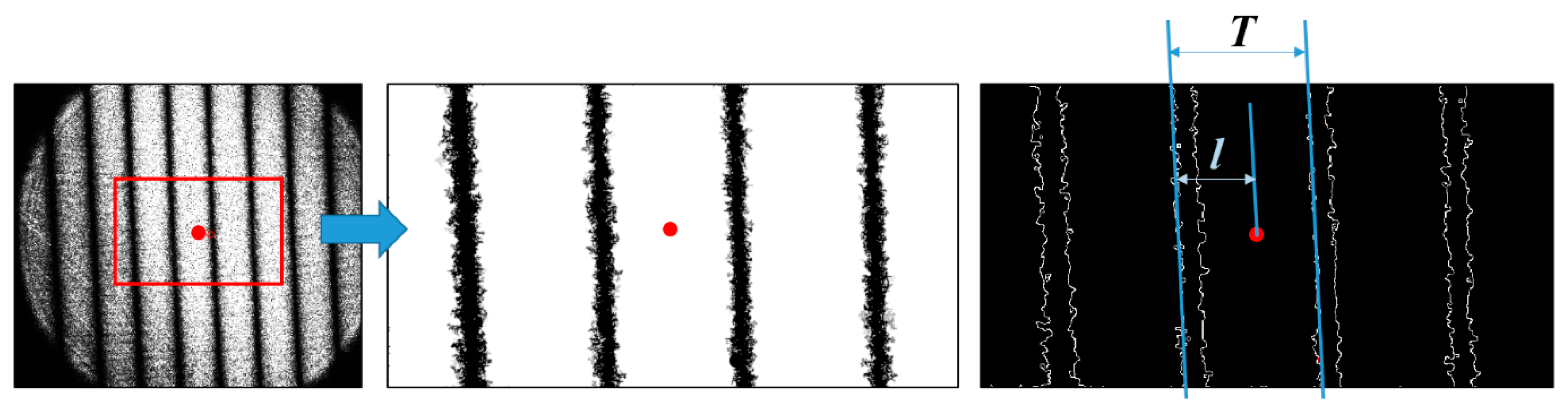
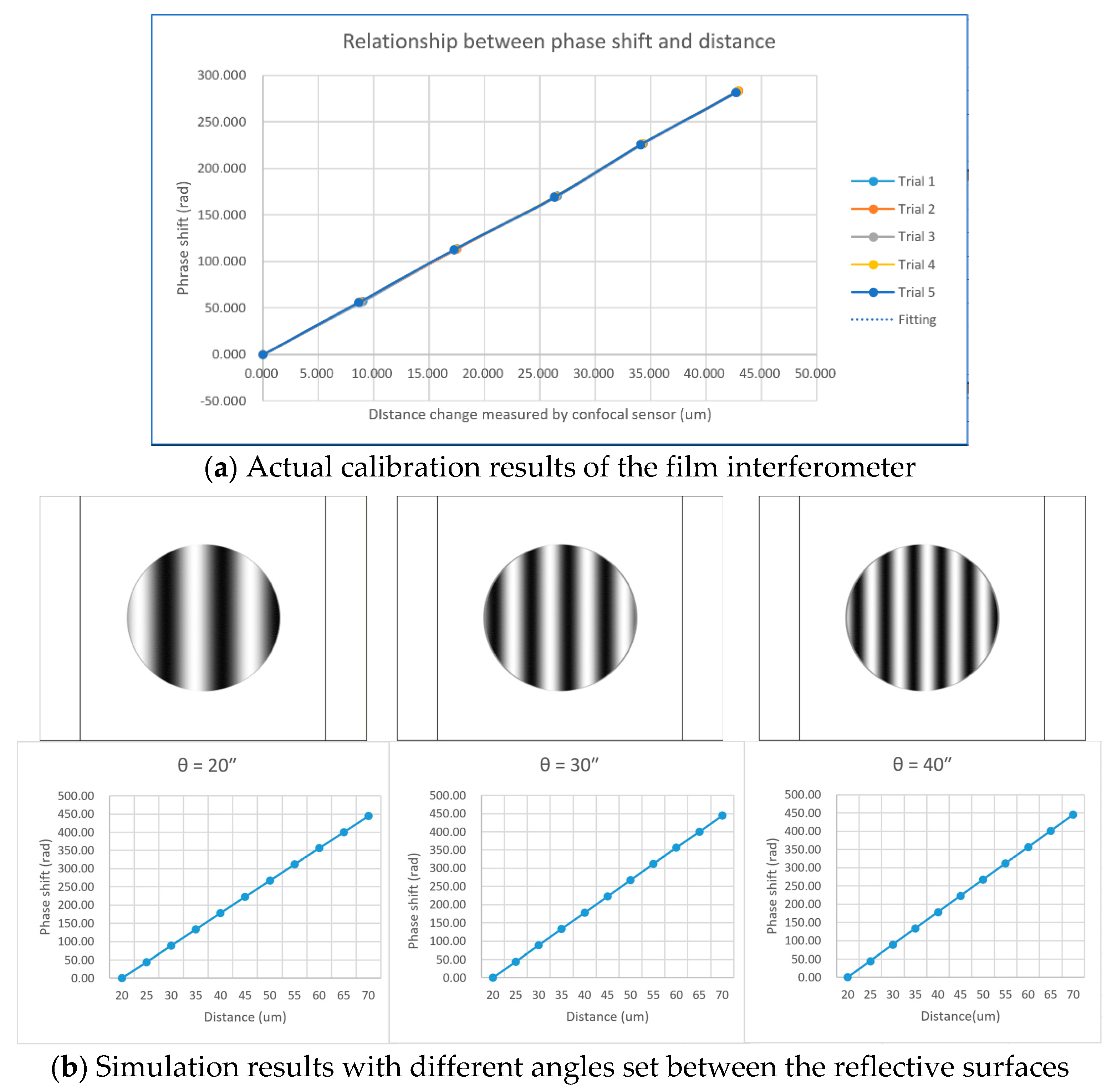
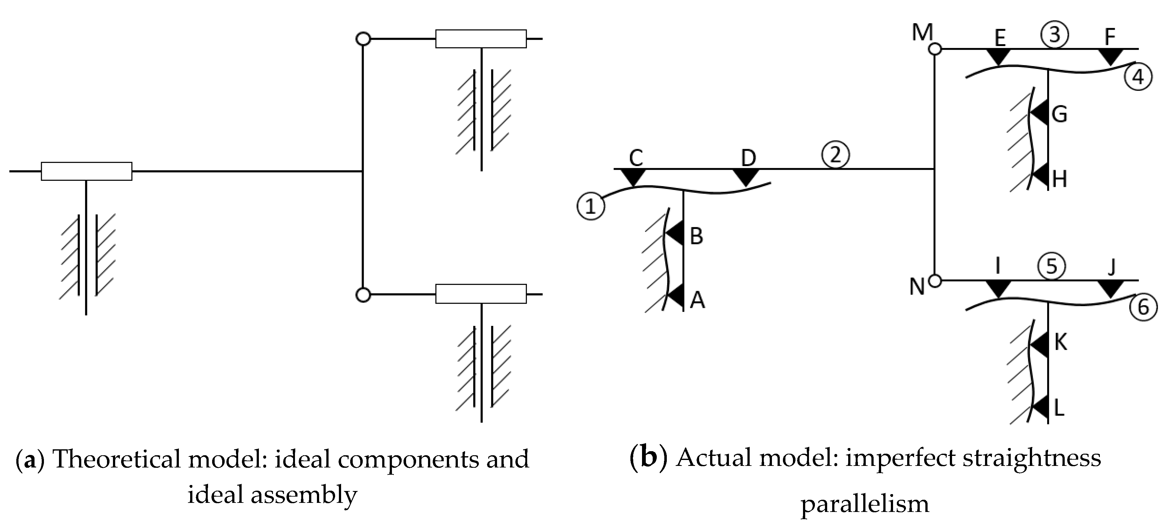
3. Motion Error Compensation Based on a Film Interferometer
- (1)
- Since the angle of the air gap was very small, FG was approximately equal to GH:
- (2)
- Since HK and IL could be seen as the same light beam in the same medium, HK was equal to IL:
- (3)
- Since LM and KN could be seen as the same light beam in different media, they had the same length of the optical path:
4. Analysis of the Degree of Freedom
- (1)
- There were one actuating module and two supporting modules in this system. Each supporting module consisted of two perpendicularly placed sliders, which were pre-assembled. This 2D sliding pair could be considered a plane contacting pair that allowed free movement in a horizontal plane despite possible in-plane placement errors.
- (2)
- The sliders were well leveled to the horizontal reference, assisted by an LVDT (Linear Variable Differential Transformer)
- (3)
- The stage top was rigidly connected with the actuating module, and it was coupled with the two supporting modules through ball hinges.
5. Experimental Verification
5.1. D Topography Measurement
5.2. Step Height Measurement in a Large Area
6. Conclusions and Discussion
Author Contributions
Funding
Conflicts of Interest
References
- Davim, J.P. Surface Integrity in Machining; Davim, J.P., Ed.; Springer: London, UK, 2010; ISBN 9781848828735. [Google Scholar]
- Whitehouse, D. Surfaces and Their Measurement; Butterworth-Heinemann: London, UK, 2004; ISBN 978-1-903996-01-0. [Google Scholar]
- Tay, C.; Wang, S.; Quan, C.; Shang, H. In situ surface roughness measurement using a laser scattering method. Opt. Commun. 2003, 218, 1–10. [Google Scholar] [CrossRef]
- Bain, L.E.; Collazo, R.; Hsu, S.; Latham, N.P.; Manfra, M.J.; Ivanisevic, A. Surface topography and chemistry shape cellular behavior on wide band-gap semiconductors. Acta Biomater. 2014, 10, 2455–2462. [Google Scholar] [CrossRef]
- Müller, T.; Kumpe, R.; Gerber, H.A.; Schmolke, R.; Passek, F.; Wagner, P. Techniques for analysing nanotopography on polished silicon wafers. Microelectron. Eng. 2001, 56, 123–127. [Google Scholar] [CrossRef]
- Lior, K. The influence of surface topography on the electromechanical characteristics of parallel-plate MEMS capacitors. J. Micromech. Microeng. 2005, 15, 1068. [Google Scholar]
- Townsend, A.; Senin, N.; Blunt, L.; Leach, R.K.; Taylor, J.S. Surface texture metrology for metal additive manufacturing: A review. Precis. Eng. 2016, 46, 34–47. [Google Scholar] [CrossRef]
- Mediratta, R.; Ahluwalia, K.; Yeo, S.H. State-of-the-art on vibratory finishing in the aviation industry: An industrial and academic perspective. Int. J. Adv. Manuf. Technol. 2016, 85, 415–429. [Google Scholar] [CrossRef]
- Yoshizawa, T. (Ed.) Handbook of Optical Metrology: Principles and Applications; CRC Press: Boca Raton, FL, USA, 2009; ISBN 978-0-8493-3760-4. [Google Scholar]
- Vorburger, T.V.; Rhee, H.G.; Renegar, T.B.; Song, J.F.; Zheng, A. Comparison of optical and stylus methods for measurement of surface texture. Int. J. Adv. Manuf. Technol. 2007, 33, 110–118. [Google Scholar] [CrossRef]
- Sandoz, P.; Tribillon, G.; Gharbi, T.; Devillers, R. Roughness measurement by confocal microscopy for brightness characterization and surface waviness visibility evaluation. Wear 1996, 201, 186–192. [Google Scholar] [CrossRef]
- Paddock, S.W. Confocal Microscopy; Humana Press: Totowa, NJ, USA, 1998; Volume 122, ISBN 1-59259-722-X. [Google Scholar]
- Viotti, M.R.; Albertazzi, A.; Fantin, A.V.; Pont, A.D. Comparison between a white-light interferometer and a tactile formtester for the measurement of long inner cylindrical surfaces. Opt. Lasers Eng. 2008, 46, 396–403. [Google Scholar] [CrossRef]
- Danzl, R.; Helmli, F.; Scherer, S. Focus variation—A robust technology for high resolution optical 3D surface metrology. J. Mech. Eng. 2011, 57, 245–256. [Google Scholar] [CrossRef]
- Ebtsam, A.; Mohammed, E.; Hazem, E. Image Stitching based on Feature Extraction Techniques: A Survey. Int. J. Comput. Appl. 2014, 99, 1–8. [Google Scholar]
- Henzold, G. Geometrical Dimensioning and Tolerancing for Design, Manufacturing and Inspection, 2nd ed.; Elsevier: Oxford, UK, 2006; ISBN 978-0750667388. [Google Scholar]
- Xue, Y.; Cheng, T.; Xu, X.; Gao, Z. High-accuracy and real-time 3D positioning, tracking system for medical imaging applications based on 3D digital image correlation. Opt. Lasers Eng. 2017, 88, 82–90. [Google Scholar] [CrossRef]
- Bradley, C. Automated Surface Roughness Measurement. Int. J. Adv. Manuf. Technol. 2000, 16, 668–674. [Google Scholar] [CrossRef]
- Sawano, H.; Gokan, T.; Yoshioka, H.; Shinno, H. A newly developed STM-based coordinate measuring machine. Precis. Eng. 2012, 36, 538–545. [Google Scholar] [CrossRef]
- Wang, S.H.; Tan, S.L.; Xu, G.; Koyama, K. Measurement of deep groove structures using a self-fabricated long tip in a large range metrological atomic force microscope. Meas. Sci. Technol. 2011, 22, 094013. [Google Scholar] [CrossRef]
- Yang, P.; Takamura, T.; Takahashi, S.; Takamasu, K.; Sato, O.; Osawa, S.; Takatsuji, T. Development of high-precision micro-coordinate measuring machine: Multi-probe measurement system for measuring yaw and straightness motion error of XY linear stage. Precis. Eng. 2011, 35, 424–430. [Google Scholar] [CrossRef]
- Hsieh, T.; Chen, P.; Jywe, W.; Chen, G.; Wang, M. A Geometric Error Measurement System for Linear Guideway Assembly and Calibration. Appl. Sci. 2019, 9, 574. [Google Scholar] [CrossRef]
- Huang, Q.; Wu, K.; Wang, C.; Li, R.; Fan, K.C.; Fei, Y. Development of an Abbe Error Free Micro Coordinate Measuring Machine. Appl. Sci. 2016, 6, 97. [Google Scholar] [CrossRef]
- Bryan, J.B. The Abbe principle revisit: An updated interpretation. Precis. Eng. 1979, 1, 129–132. [Google Scholar] [CrossRef]
- Okuyama, E.; Akata, H.; Ishikawa, H. Multi-probe method for straightness profile measurement based on least uncertainty propagation (1st report): Two-point method considering cross-axis translational motion and sensor’s random error. Precis. Eng. 2010, 34, 49–54. [Google Scholar] [CrossRef]
- Chen, X.; Sun, C.; Fu, L.; Liu, C. A novel reconstruction method for on-machine measurement of parallel profiles with a four-probe scanning system. Precis. Eng. 2019, 59, 224–233. [Google Scholar] [CrossRef]
- Jin, T.; Ji, H.; Hou, W.; Le, Y.; Shen, L. Measurement of straightness without Abbe error using an enhanced differential plane mirror interferometer. Appl. Opt. 2017, 56, 607–610. [Google Scholar] [CrossRef] [PubMed]
- Feng, W.L.; Yao, X.D.; Azamat, A.; Yang, J.G. Straightness error compensation for large CNC gantry type milling centers based on B-spline curves modeling. Int. J. Mach. Tools Manuf. 2015, 88, 165–174. [Google Scholar] [CrossRef]
- Chen, B.; Xu, B.; Yan, L.; Zhang, E.; Liu, Y. Laser straightness interferometer system with rotational error compensation and simultaneous measurement of six degrees of freedom error parameters. Opt. Express 2015, 23, 9052–9073. [Google Scholar] [CrossRef] [PubMed]
- Jäger, G.; Hausotte, T.; Manske, E.; Büchner, H.J.; Mastylo, R.; Dorozhovets, N.; Hofmann, N. Nanomeasuring and nanopositioning engineering. Measurement 2010, 43, 1099–1105. [Google Scholar] [CrossRef]
- Fan, K.-C.; Cheng, F. “The System and Mechatronics of a Pagoda Type Micro-CMM”, Special Issue on Precision Micro- and Nano-Metrology for Nanomanufacturing. Int. J. Nanomanufacturing 2011, 8, 107–112. [Google Scholar]
- Wirotrattanaphaphisan, K.; Buajarern, J.; Butdee, S. Uncertainty evaluation for absolute flatness measurement on horizontally aligned fizeau interferometer. J. Phys. Conf. Series 2019, 1183, 012009. [Google Scholar] [CrossRef]
- Vermeulen, M.; Rosielle, P.C.J.N.; Schellekens, P.H.J. Design of a high-precision 3D-coordinate measuring achine. CIRP Ann. Manuf. Technol. 1998, 47, 447–450. [Google Scholar] [CrossRef]
- Fan, K.C.; Fei, Y.T.; Yu, X.F.; Chen, Y.J.; Wang, W.L.; Chen, F.; Liu, Y.S. Development of a low-cost micro-CMM for 3D micro/nano measurements. Meas. Sci. Tech. 2006, 17, 524–532. [Google Scholar] [CrossRef]
- Uicker, J.J.; Pennock, G.R.; Shigley, J.E. Theory of Machines and Mechanisms; Oxford University Press: New York, NY, USA, 2003. [Google Scholar]
- Fu, S.; Cheng, F.; Tegoeh, T. A Non-Contact Measuring System for In-Situ Surface Characterization Based on Laser Confocal Microscopy. Sensors 2018, 18, 2657. [Google Scholar] [CrossRef]
- Yu, Q.; Zhang, K.; Cui, C.; Zhou, R.; Cheng, F. Calibration of a Chromatic Confocal Microscope for Measuring a Colored Specimen. IEEE Photonics J. 2018, 10, 6901109. [Google Scholar] [CrossRef]
- Fu, S.; Cheng, F.; Tegoeh, T.; Liu, M. Development of an Image Grating Sensor for Position Measurement. Sensors 2019, 19, 4986. [Google Scholar] [CrossRef] [PubMed]


| Components | Specifications |
|---|---|
| Camera | Basler acA2000-165um, frame rate 165 fps, resolution 2048 × 1088 (2 MP) |
| Lens | Moritex ML - MC50HR, 0.8×, focal length 50mm |
| Right-angle prism | 25.4 mm × 25.4 mm × 25.4 mm, K9 glass, refractive index 1.5163 |
| Sample | Ra (µm) | Deviation (µm) | Deviation (%) | Rq (µm) | Deviation (µm) | Deviation (%) | ||
|---|---|---|---|---|---|---|---|---|
| HQU | Mahr XR20 | HQU | Mahr XR20 | |||||
| 1 | 0.589 | 0.602 | 0.602 | 2.2% | 0.735 | 0.714 | 0.021 | 2.9% |
| 2 | 1.493 | 1.471 | 1.471 | 1.5% | 1.746 | 1.737 | 0.009 | 0.5% |
| 3 | 2.736 | 2.728 | 2.728 | 0.2% | 3.238 | 3.234 | 0.004 | 0.1% |
| 4 | 5.842 | 5.810 | 5.810 | 0.6% | 6.753 | 6.728 | 0.025 | 0.4% |
| Location 1 | Location 2 | Location 3 | Location 4 | |
|---|---|---|---|---|
| 100.1910 | 100.1073 | 99.9984 | 99.9834 | |
| Step height measured (µm) | 100.1284 | 100.2008 | 99.9857 | 99.9637 |
| 100.1179 | 100.1414 | 99.9284 | 99.9806 | |
| (Nominal: 100.080 µm) | 100.2042 | 100.1783 | 100.0852 | 100.0523 |
| 100.2156 | 100.1290 | 99.985 | 100.0361 | |
| Average (µm) | 100.1715 | 100.1514 | 99.9965 | 100.0032 |
| Repeatability σ (µm) | 0.0451 | 0.0378 | 0.05648 | 0.03859 |
| Reproducibility σ’ (µm) | 0.09293 | |||
| Technologies | Measurement Resolution | Measurement Area | Probe | Motion Error Compensation |
|---|---|---|---|---|
| Confocal microscopy | ~10 nm | ~1 mm | Optical | No |
| coherence scanning interferometry | ~1 nm | ~1 mm | Optical | No |
| Focus variation | ~20 nm | ~1 mm | Optical | No |
| Stylus profilometry | ~1 nm | ~100 mm | Contact | No |
| HQU developed system | ~10 nm | 100 mm | Optical | Yes |
| STM with high-precision stage [19] | Sub-nanometer | ~1 mm | STM | Not stated |
| AFM with high-precision stage [20] | Sub-nanometer | ~1 mm | AFM | Yes |
© 2020 by the authors. Licensee MDPI, Basel, Switzerland. This article is an open access article distributed under the terms and conditions of the Creative Commons Attribution (CC BY) license (http://creativecommons.org/licenses/by/4.0/).
Share and Cite
Cheng, F.; Zou, J.; Su, H.; Wang, Y.; Yu, Q. A Differential Measurement System for Surface Topography Based on a Modular Design. Appl. Sci. 2020, 10, 1536. https://doi.org/10.3390/app10041536
Cheng F, Zou J, Su H, Wang Y, Yu Q. A Differential Measurement System for Surface Topography Based on a Modular Design. Applied Sciences. 2020; 10(4):1536. https://doi.org/10.3390/app10041536
Chicago/Turabian StyleCheng, Fang, Jingwu Zou, Hang Su, Yin Wang, and Qing Yu. 2020. "A Differential Measurement System for Surface Topography Based on a Modular Design" Applied Sciences 10, no. 4: 1536. https://doi.org/10.3390/app10041536
APA StyleCheng, F., Zou, J., Su, H., Wang, Y., & Yu, Q. (2020). A Differential Measurement System for Surface Topography Based on a Modular Design. Applied Sciences, 10(4), 1536. https://doi.org/10.3390/app10041536