Abstract
This paper presents a review of state-of-the-art micro-electro-mechanical-systems (MEMS) acoustic emission (AE) sensors. MEMS AE sensors are designed to detect active defects in materials with the transduction mechanisms of piezoresistivity, capacitance or piezoelectricity. The majority of MEMS AE sensors are designed as resonators to improve the signal-to-noise ratio. The fundamental design variables of MEMS AE sensors include resonant frequency, bandwidth/quality factor and sensitivity. Micromachining methods have the flexibility to tune the sensor frequency to a particular range, which is important, as the frequency of AE signal depends on defect modes, constitutive properties and structural composition. This paper summarizes the properties of MEMS AE sensors, their design specifications and applications for detecting the simulated and real AE sources and discusses the future outlook.
1. Introduction
Acoustic emission (AE) is based on the detection of propagating elastic waves released by sudden stress-strain change in materials. Since the development of high-resolution instrumentation and data analysis tools, the AE method has been applied as a nondestructive evaluation tool in a variety of applications [1]. AE sensors form the primary link in detecting defects as shown in Figure 1. The energy released by an AE source propagates through the medium and reaches the AE sensor, which converts mechanical signal into electrical signal, defined as AE signal. Conventional AE sensors are made of bulky piezoelectric ceramics. While they have been used successfully in many applications, manual manufacturing, cost and size require moving the technology towards automated mass manufacturing of AE sensors with increased reliability, reduced cost and size.
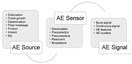
Figure 1.
The simplified chain of acoustic emission (AE) sensing—AE sensor bridging AE source and AE signal.
Micro-electro-mechanical-systems (MEMS) are based on designing and manufacturing sensors and actuators using micromachining techniques (e.g., surface and bulk micromachining) which allow mass manufacturing with repeatable intrinsic characteristics. MEMS have enabled the design of sensors and systems using micromachining techniques since 1990s [2]. The application of the MEMS concept into AE sensing was first introduced by Schoess and Zook in 1998 [3]. Since then, there are several examples of piezoresistive, capacitive and piezoelectric MEMS AE sensors reported in the literature. With the introduction of a thin-film piezoelectric layer into MEMS manufacturing, potential towards to a commercial success for piezoelectric MEMS AE sensors increased. The first example of piezoelectric MEMS AE sensor was reported by Feng and Tsai in 2010 [4].
In this review article, the physical factors inherent to AE sensing and contributing to the design of MEMS AE sensors are discussed. The main characteristics of MEMS AE sensors such as resonant frequency, bandwidth/quality factor, sensitivity and other specifications pertinent to the transduction principles are presented. Transduction principles commonly used in MEMS AE sensing, including piezoresistive, capacitive (i.e., electrostatic) and piezoelectric, are discussed. Common MEMS geometries in the forms of beam or diaphragm and their design equations to tune to different frequencies are discussed. The history of MEMS AE sensors reported in the literature is presented. Conclusions and future outlook are discussed in the final section.
2. Intrinsic Characteristics of AE Method Controlling AE Sensor Design
The AE method is a well-known nondestructive evaluation (NDE) method for (a) detecting the initiation of damage, (b) pinpointing the location of damage site, (c) qualitatively assessing the severity of damage and (d) classifying the damage mode using pattern recognition tools. Typically, resonant type AE sensor with narrowband frequency range is selected for (a), (b) and (c). While there are numerous examples using resonant AE sensors for the classification of damage modes, the proper source classification requires wideband or multifrequency AE sensors.
The AE source (related to energy release) and the structural medium carrying AE source to AE sensor (related to attenuation) control tuning the AE sensor into the right frequency, bandwidth, directional dependence and sensitivity. Once the target AE source and energy release are identified, the AE sensor characteristics can be defined. The AE sources depend on the materials’ composition. For instance, crack growth is a common AE source in metals while fiber breakage, matrix cracking and delamination are common AE sources in composites. Table 1 shows examples of AE sources in solids. As the structural medium and the defect mode are related, AE sensor should be designed by taking their interaction into consideration. As shown in Table 1, when a material has porous, anisotropic and viscoelastic properties, a low-frequency AE sensor is preferred to reduce the influence of attenuation and increase signal-to-noise ratio [5].

Table 1.
Common AE sources in solids and typical AE sensors selected.
Different defects generate different strain energy releases, which influence the selection of AE sensor sensitivity. Most literature selects the AE sensor based on previous literature, space limitation that controls the size of the specimen and available off-the-shelf sensors. A more physics-based approach is needed for selecting the proper AE sensor for sensing a particular defect in a material and energy release rate. In that aspect, state-of-the-art numerical models are combined with fracture mechanics in recent studies [14,15,16].
AE sensors are designed as resonant or broadband type. Resonant AE sensors, typically in the range of 20–500 kHz, have high quality (Q) factor (low damping), leading to narrow frequency bandwidth and high sensitivity. As they modify the input signal, they have limited applications for AE source characterization. However, they perform well in localizing AE sources in highly dispersive media (exhibiting frequency-dependent wave velocity) and pinpointing the initiation of the earliest stage of damage before visually seen. As MEMS AE sensors have smaller footprints than conventional AE sensors, they are typically designed as resonators to amplify the signal-to-noise ratio. Broadband AE sensors have a low Q factor, high damping, wide frequency bandwidth and low sensitivity. As they do not disturb the input signal, they are successfully implemented in identifying damage modes and source depth based on modal analyses. Figure 2 shows the comparison of a bulky piezoelectric AE sensor and a piezoelectric MEMS AE sensor. The conventional sensor includes piezoelectric ceramic sandwiched between electrodes and protected with wear plate and protection case. The piezoelectric MEMS AE sensor is made of a resonating silicon microstructure and a thin piezoelectric layer, which is mounted on a ceramic package. There is significant reduction in size and weight of MEMS AE device as compared to the conventional AE sensor.
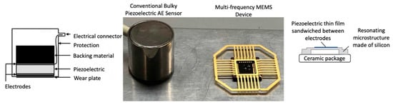
Figure 2.
The comparison of conventional piezoelectric bulky AE sensor and piezoelectric micro-electro-mechanical-systems (MEMS) AE sensor designed by Ozevin’s research group.
3. Transduction Principles of MEMS AE Sensors
The dynamic input signal (displacement, velocity or acceleration) at the position of the AE sensor is converted into an electrical signal using three main transduction principles: piezoresistivity, capacitance and piezoelectricity. The geometric configurations can be lumped mass or distributed mass (i.e., diaphragm), as shown in Figure 3.
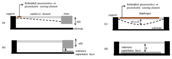
Figure 3.
Different geometries and sensing configurations, (a) lumped mass + cantilever beam with piezoelectric or piezoresistive element, (b) lumped mass + cantilever beam with capacitive sensing, (c) distributed mass on a diaphragm with piezoelectric or piezoresistive element, (d) distributed mass on a diaphragm with capacitive sensing.
3.1. Piezoresistive MEMS AE Sensors
Smith [17] demonstrated the piezoresistivity property of silicon, which has been used as a transduction mechanism for mechanical MEMS sensors since then. The change in resistivity is proportionate to stress as follows [18]:
where is electrical resistance, is piezoresistivity coefficient, which depends on the crystal orientation and the dopant level, and is stress. The electrical resistance between two ends of a resistor is measured by
where is length, is cross-sectional area [19]. The change in resistance is related to
Assuming that the resistor is exposed to uniaxial strain, Equation (3) becomes
where is longitudinal strain, is Poisson’s ratio. The sensitivity is measured by the gauge factor () as
If the strain and the direction of current are both in longitudinal direction on <100> plane, then
where is Young’s Modulus of silicon. Here, represents . Combining Equations (5) and (6),
The n-type dopant would result in higher gauge factor as value is −102.2 × 10⁻¹¹ Pa−1, while it is 6.6 × 10⁻¹¹ Pa−1 for the p-type dopant. However, the p-type silicon piezoresistor has higher conductivity than the n-type silicon piezoresistor, which reduces the effect of temperature to the output signal [20]. The temperature dependence of piezoresistivity coefficients influences the measurement [21]. Therefore, temperature compensation approaches should be applied [22].
3.2. Capacitive MEMS AE Sensors
A capacitance is made of two conductors with opposite charges. A parallel plate capacitor is the most common configuration for AE sensing. The diaphragm forming the moving electrode of parallel plate capacitor can be built using a hexagonal [23], circular [24], square [25] or rectangular [26] shape.
Capacitance change due to dynamic stimulus is detected via change in capacitance (), which is related to dielectric constant (), overlapping area () or gap () between two capacitive layers. The capacitance between two parallel plates is measured by
As shown in Figure 3d, one layer is deposited on the substrate and the other layer is free to vibrate under inertial force. The change in capacitance is related to
If the dominant factor to capacitance change is gap change (), the produced displacement current () is calculated as
where is DC bias voltage, is time and is dielectric constant of air [25]. The operation of capacitive MEMS sensors requires constant DC bias voltage, which may introduce long-term durability challenges [27] in AE applications.
Figure 4 shows an example of a differential MEMS AE sensor achieved by designing two different gaps between capacitive layers that change due to in-plane excitation. The geometry can be modified to have different mass and spring elements, and multiple individual units can be connected to increase total capacitance and current output, which improves the signal-to-noise ratio. Capacitive MEMS AE sensors have advantages of large bandwidth, sensitivity, efficiency, integrated circuit compatibility and geometry flexibility.
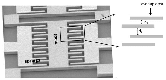
Figure 4.
An example of a capacitive MEMS AE sensor for in-plane wave sensing [28].
The important variables for designing capacitive MEMS AE sensors are:
- Fundamental frequency, , which is controlled by stiffness and mass of microstructure. The geometry can be varied to tune to a particular frequency.
- Collapse voltage, which is defined as the bias voltage causing the failure of membrane. The value depends on stiffness, gap and overall area [29]. As the sensitivity increases with higher as shown in Equation (10), the design with higher collapse voltage improves the signal-to-noise ratio.
- Quality factor controls the bandwidth of a capacitive MEMS sensor. Quality factor depends on squeeze film damping between stationary and moving layers. High quality factor improves signal-to-noise ratio while it reduces the bandwidth. Squeeze film damping occurs due to the pressure of thin viscous fluid between two layers. The resonant frequency is also influenced by the damping level in the atmospheric condition [23,30].
- Dielectric charging, which is caused by the accumulation of unwanted charges stored and trapped on the dielectric surface [27]. This can increase the stiction of two layers, leading to permanent device failure. The failure can be prevented by depositing dielectric posts or a layer between two electrodes [21].
Post-manufacturing packaging of capacitive MEMS AE sensors has limited robustness. Wafer-level packaging can be adapted from capacitive MEMS ultrasonic transducers [31].
3.3. Piezoelectric MEMS AE Sensors
Since the development of thin piezoelectric film deposition on a substrate, piezoelectric MEMS sensors have been designed for sensing and actuating [32]. The thin-film piezoelectric layers have size constraints, stress from substrate, epitaxial growth affecting dependence on crystal orientation and substrate preparation to be compatible with piezoelectric thin-film [33]. The most common piezoelectric MEMS are resonating devices made of a piezoelectric layer deposited on a membrane operating at its resonance frequency. The piezoelectric AE sensor operates in the direct effect, which means that a mechanical strain or stress causes an electrical displacement. The coupled mechanical and electrical domains of bulk piezoelectric materials apply to thin piezoelectric films as
where and are strain and stress tensors, and are electric field and displacement, represents elastic compliance and are piezoelectric coefficients. For thin-film piezoelectric MEMS devices, the most common coefficients are and , which are related to the electric field in 3 direction to strain, either in the same direction (3) or the orthogonal direction (1 or 2 due to symmetry) [34,35]. The directions 1, 2 and 3 are shown in Figure 5. The most important materials and geometric properties for sensing are piezoelectric coefficients, electromechanical coupling coefficient, mechanical quality factor, resonant frequency and residual stress.
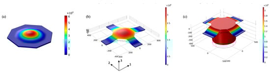
Figure 5.
Three configurations to tune the resonant frequency, (a) diaphragm anchored around circumference to tune at MHz range, (b) diaphragm connected with flexible beams to tune the 100–500 kHz range, (c) silicon mass connected with flexible beams to tune less than 100 kHz. The color scale indicates the total displacement in micrometers.
- Piezoelectric coefficient and doping direction depend on ferroelectric (e.g., PZT) or nonferroelectric (e.g., AlN) materials. Ferroelectric materials are doped after deposition, while the doping orientation of nonferroelectric materials is controlled during the deposition [34]. Piezoelectric coefficients of common piezoelectric thin films can be found in [35].
- Electromechanical coupling factor is the ratio of the mechanical energy converted to the input electrical energy of the piezoelectric material. It can be calculated by motional capacitance and passive capacitance.
- Quality factor measures the mechanical damping of a microstructure where a high quality factor is needed for MEMS resonators [35]. Piezoelectric design has a higher quality factor than capacitive design, caused by squeeze film damping. The quality factor can be extracted from the impedance curve and half-power bandwidth formula aswhere is the resonance frequency and is the difference of two frequencies with magnitude of [36].
- Resonant frequency is controlled by mass and stiffness of microstructure. Further discussion is presented in the next section.
- The residual stress causing pretention to circular plate design can influence the resonant frequency [37]. If a thin diaphragm is selected for designing a low-frequency sensor (less than 200 kHz), geometric nonlinearities should be considered due to high aspect ratio of diameter to thickness [38]. To reduce the aspect ratio for designing low frequency piezoelectric resonators, Kabir et al. [39] designed a membrane connected with four beam elements and a mass made of an entire silicon substrate to reduce the resonant frequency of the microstructure as shown in Figure 5.
4. MEMS AE Sensor Geometries
Typical MEMS AE sensors are designed using a cantilever beam or plate (i.e., diaphragm). Figure 3 and Figure 5 show common configurations used in the design of MEMS AE sensors. The cantilever beam can be designed as lumped mass or distributed mass models. If the lump mass model is considered, the fundamental frequency is calculated by
where is transverse stiffness of cantilever beam and is lump mass. Assuming the rotation at the cantilever beam and mass is restrained, stiffness is calculated by where is the moment of inertia, is the cantilever length.
If the distributed mass model is considered, the fundamental frequency is calculated by [40]
where is coefficient depending on mode number (e.g., 3.516 for the first mode, 22.03 for the second mode) and is cross sectional area.
The diaphragm shapes can be circular, hexagonal, octagonal or square. Analytical solutions of circular and square plates exist. Each model frequency of rectangular plates for simply supported boundary conditions at all sides is calculated by
where , are integers (e.g., 1 for the first mode), are two edge distances. The equation for circular plates is
where depends on the mode number. The value is 3.01146 for the first mode, 6.20540 for the second mode etc. [41]. For instance, the circular microstructure made of 10 μm silicon with the material properties as , , , Figure 6 shows the relationship between fundamental frequency and the diameter of microstructure. The diameter of a 10 μm-thick silicon microstructure should be between 560−340 μm to tune the sensor between 100–300 kHz.
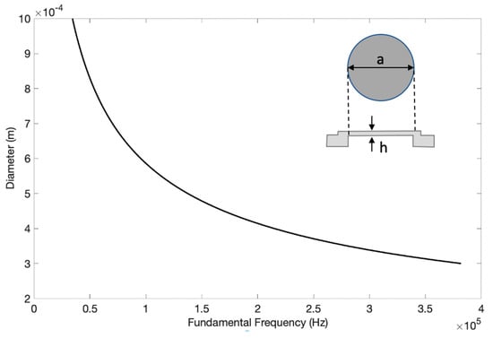
Figure 6.
The relationship between fundamental frequency and diameter of a 10 μm silicon microstructure with simply supported boundary condition.
For complex geometries without analytical formulation, the frequency responses are obtained by finite element models. While conventional bulky AE sensors are calibrated using ASTM standards [42,43], the properties of MEMS AE sensors are extracted from electromechanical testing. The resonant frequency of MEMS AE sensors can be measured through impedance measurement. Figure 7 shows an example of admittance and phase values of a MEMS AE sensor designed with a mass connected with four beams [39]. The measurement was conducted using an impedance analyzer in atmospheric pressure. The features of resonant frequency and quality factor can be extracted from the impedance measurement.
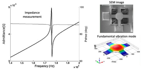
Figure 7.
An example of admittance and phase plots of a MEMS AE sensor tuned near 170 kHz.
The sensor geometry configured for each transduction principle influences the bandwidth of MEMS AE sensors. As capacitive sensors require two parallel electrodes, they have a lower quality factor as compared to piezoresistive and piezoelectric MEMS AE sensors. The quality factor of a capacitive sensor is increased by adding additional etch holes to provide air flow between two parallel plates [25]. The bandwidth can be widened by increasing the damping via adding backing material, which reduces the response magnitude of the vibrating microstructural element. For the assumption of lumped mass model (valid assumption for the design with a single dominating mode shape), the displacement response of linear elastic system can be calculated as
where is the displacement, is the applied force, is the lumped stiffness and is the Laplace variable [44]. The solution is controlled by stiffness, circular frequency and quality factor. If the quality factor increases, the damping effect is reduced. The conversion of displacement into electrical signal depends on the transduction principle.
5. History of MEMS AE Sensors, 1998–2020
The first example of MEMS application to AE sensing dates back to 1998. Schoess and Zook designed a resonating microbeam tuned to 312 kHz fundamental frequency [3]. They deposited piezoresistive material to the edge of a micro beam. Kawashima et al. [45] advanced the piezoresistive sensing of AE with a silicon cantilever to tuning lengths of individual cantilever elements to different frequencies to increase the frequency bandwidth. Each design still behaved as an individual resonator. The other example of a piezoresistive MEMS AE sensor is n-type piezoresistive area generated on Si layer [46]. Table 2 summarizes the piezoresistive MEMS AE sensors and their specifications.
Table 2.
Piezoresistive MEMS AE sensors and their specifications.
In 2006, Ozevin et al. demonstrated capacitive MEMS AE sensors made of resonating suspending silicon on a stationary silicon layer [25]. They tuned individual sensors to particular frequencies in the range of 100 to 500 kHz. To reduce the influence of sequence film damping, square etch hole spacing was reduced to 13 μm spacing. Unit cells of 49 to 100 were combined in series to increase the total capacitance and sensitivity. While the MEMS AE sensors were applied to detect the crack growth successfully, the signal-to-noise ratio was significantly lower than conventional piezoelectric AE sensors. Harris et al. [47] improved the sensitivity of capacitive MEMS AE sensors by introducing rectangular etch holes to reduce the squeeze film damping. Both sensors were manufactured using the surface micromachining method, which limits the maximum thickness of the resonating element to a few micrometers. To address the thickness limitation of the surface micromachining method, Saboonchi and Ozevin [26] utilized an electroplating technique to build thick metal layer as the resonating layer of a capacitive MEMS AE sensor. They tuned two resonators to 68 and 149 kHz. Similar to Harris et al. (2011), they used rectangular etch holes to reduce the squeeze film damping. They also added silicon nitride (0.35 μm-thick) between the stationary layer and the resonating layer in addition to 1.1 μm air, which reduced the stiction problem of two parallel capacitors. The sensitivity of the capacitive MEMS sensor was greatly improved as compared to earlier versions. Batuad et al. [24] studied circular capacitive MEMS AE sensors to design multifrequency individual sensors for improving the sensor bandwidth. They demonstrated the signal-to-noise ratio of 20 dB at the resonance frequency. Table 3 summarizes the capacitive MEMS AE sensors and their specifications.
Table 3.
Capacitive MEMS AE sensors and their specifications.
While capacitive MEMS AE sensors have advantages such as flexible geometry design and the integration with on-chip electronics, the need of constant DC bias is a limiting factor for long-term AE sensing, especially wireless applications. With Feng and Tsai [4], the research on piezoelectric MEMS AE sensors has started. They built a piezoelectric AE sensor using a corrugated PVDF mechanism. The sensor had wideband frequency range with the sensitivity of 1 mV/nm. The same research group designed a piezoelectric MEMS AE sensor by depositing PZT film on a cantilever sensing structure [48]. A thermoresponsive actuator was added to increase the contact pressure. The application of this sensor was demonstrated on monitoring knee failures [49]. Chen et al. [50] designed the first flexible MEMS AE sensor by depositing PZT nanofibers on a composite membrane using the electrosplitting method. The sensor exhibited anisotropic sensitivity, which could be advantageously used to understand the direction of the AE signal. While signal-to-noise is a concern, being a flexible geometry increases its use in conformal surfaces and weight-restricted applications. Ali and Prasad [51] designed a low-frequency (~78.9 kHz resonance) MEMS AE sensor for sound waves by depositing a 3.0 μm-thick ZnO layer on a square silicon diaphragm. They recently studied the optimized fabrication and annealing temperature [52]. Kabir et al. [39] designed multifrequency MEMS sensors by depositing a 0.5 μm-thick AlN piezoelectric layer on silicon and utilizing PiezoMUMPs provided by MEMSCAP. A low-frequency sensor tuned to 35 kHz was designed by utilizing the entire silicon substrate as a mass, which reduced the total size of the sensor to less than 1 mm. The sensors exhibited a very high quality factor, which could be advantageous for source localization in dispersive media by detecting a single frequency and reducing the effect of low-frequency friction emissions by behaving as a mechanical filter. They showed that amplitude-to-size ratios of an R15 sensor (resonant frequency near 150 kHz, manufactured by MISTRAS Group Inc., Princeton Junction, NJ, USA) and piezoelectric MEMS AE tuned near 200 kHz are 1.24 mV/mm3 and 99.59 mV/mm3, respectively. Table 4 summarizes the piezoelectric MEMS AE sensors using silicon as a microstructure and their specifications.
Table 4.
Piezoelectric MEMS AE sensors and their specifications.
6. Conclusions and Future Outlook
There is an increasing trend of utilizing piezoelectric MEMS resonators for the design of AE sensors. While MEMS have the geometric flexibility in tuning the sensor frequency to a particular value with narrow bandwidth, mass manufacturing and low-cost design, the demonstrations of MEMS AE sensors for detecting real AE sources, rather than stimulations and field deployment, are limited. While the sensitivity of MEMS AE sensors needs to be improved, they are applicable to detecting AE sources with high energy release rates such as wire breaks. A robust packaging design encapsulated against a harsh environment for long-term field deployment is needed.
A monolithic integration of multiple frequencies by combining individual resonators could overcome the sensitivity limitation. As an example, two highly resonant MEMS piezoelectric sensors are connected in an array such that the total response is increased by the constructive interference of carefully selected frequencies. Figure 8 shows individual responses of 200 kHz and 300 kHz sensors designed by PiezoMUMPs, and their combined response using a single channel output. The sensors are excited by a chirp signal in the range of 100–400 kHz. The frequency spectrum of the combined signal clearly shows two distinct frequencies with the constructive interference, such that the total response is a simple summation of two individual responses.
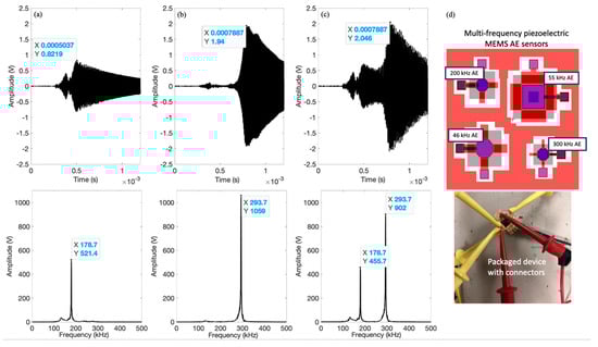
Figure 8.
Single channel, multifrequency, piezoelectric MEMS AE sensor for boosting the sensitivity, (a) connecting only 200 kHz sensor in time and frequency domains, (b) connecting only 300 kHz sensor in time and frequency domains, (c) series connection of 200 kHz + 300 kHz sensors in time and frequency domains, (d) the layout of MEMS device and the packaged configuration.
In summary, while there are numerous examples of MEMS AE sensors in the literature, they have been evaluated in a laboratory environment, mostly using simulated AE sources. The transition of MEMS AE sensors into practice requires (a) comparable sensitivity to conventional AE sensors, (b) robust packaging to function well in harsh environments with long-term durability, (c) the ability to detect actual AE sources in a laboratory environment and (d) field deployment for side-to-side comparison with conventional AE sensors.
Funding
This research was funded by National Science Foundation under Award No. IIP 2016444 entitled “PFI-TT: Multi-Frequency Acoustic Device for Rapid Infrastructure Damage Diagnostics”.
Conflicts of Interest
The author declares no conflict of interests.
References
- Drouillard, T.F. A History of Acoustic Emission. J. Acoust. Emiss. 1995, 14, 1–34. [Google Scholar]
- Liu, C. Foundations of MEMS; Pearson Prentice Hall: Upper Saddle River, NJ, USA, 2006. [Google Scholar]
- Schoess, J.N.; Zook, J.D. Test Results of Resonant Integrated Microbeam Sensor (RIMS) for Acoustic Emission Monitoring. J. Intell. Mater. Syst. Struct. 1998, 9, 947–951. [Google Scholar] [CrossRef]
- Feng, G.H.; Tsai, M.Y. Acoustic Emission Sensor with Structure-enhanced Sensing Mechanism based on Micro-embossed Piezoelectric Polymer. Sens. Actuators A Phys. 2010, 162, 100–106. [Google Scholar] [CrossRef]
- Ono, K. Acoustic Emission, 2nd ed.; Rossing, Ed.; Springer Handbook of Acoustics: Berlin/Heidelberg, Germany, 2014; Chapter 30. [Google Scholar]
- Vinogradov, A.; Yasnikov, I.S.; Merson, D.L. Phenomenological approach towards modelling the acoustic emission due to plastic deformation in metals. Scr. Mater. 2019, 170, 172–176. [Google Scholar] [CrossRef]
- Aggelis, D.G.; Kordatos, E.Z.; Matikas, T.E. Acoustic emission for fatigue damage characterization in metal plates. Mech. Res. Commun. 2011, 38, 106–110. [Google Scholar] [CrossRef]
- Vanniamparambil, P.A.; Guclu, U.; Kontsos, A. Identification of crack initiation in aluminum alloys using acoustic emission. Exp. Mech. 2015, 55, 837–850. [Google Scholar] [CrossRef]
- Leone, F.A.; Ozevin, D.; Awerbuch, J.; Tan, T.M. Detecting and Locating Damage Initiation and Progression in Full-scale Sandwich Composite Fuselage Panels using Acoustic Emission. J. Compos. Mater. 2012, 47, 1643–1664. [Google Scholar] [CrossRef]
- Sause, M.G.R.; Horn, S. Quantification of the Uncertainty of Pattern Recognition Approaches Applied to Acoustic Emission Signals. J. Nondestruct. Eval. 2013, 32, 242–255. [Google Scholar] [CrossRef]
- Shahidan, S.; Pulin, R.; Bunnori, N.M.; Holford, K.M. Damage classification in reinforced concrete beam by acoustic emission signal analysis. Constr. Build. Mater. 2013, 45, 78–86. [Google Scholar] [CrossRef]
- Perrin, M.; Yahyaoui, I.; Gong, X. Acoustic monitoring of timber structures: Influence of wood species under bending loading. Constr. Build. Mater. 2019, 208, 125–134. [Google Scholar] [CrossRef]
- Michlmayr, G.; Cohen, D.; Or, D. Source and characteristics of acoustic emissions from mechanically stressed granular media—A review. Earth Sci. Rev. 2012, 112, 97–114. [Google Scholar] [CrossRef]
- Sause, M.G.R.; Horn, S. Simulation of Acoustic Emission in Planar Carbon Fiber Reinforced Plastic Specimens. J. Nondestruct. Eval. 2010, 29, 123–142. [Google Scholar] [CrossRef]
- Sause, M.G.R.; Richler, S. Finite Element Modelling of Cracks as Acoustic Emission Sources. J. Nondestruct. Eval. 2015, 34, 1–13. [Google Scholar] [CrossRef]
- Cuadra, J.A.; Baxevanakis, K.P.; Mazzotti, M.; Bartoli, I.; Kontsos, A. Energy Dissipation via Acoustic Emission in Ductile Crack Initiation. Int. J. Fract. Mech. 2016, 199, 89–104. [Google Scholar] [CrossRef]
- Smith, C.S. Piezoresistance Effect in Germanium and Silicon. Phys. Rev. 1994, 94, 42–49. [Google Scholar] [CrossRef]
- Nathan, A.; Baltes, H. Microtransducer CAD: Physical and Computational Aspects; Springer: Wien, Austria; New York, NY, USA, 1999. [Google Scholar]
- Doll, J.S.; Pruitt, B.L. Piezoresistor Design and Applications; Springer: Berlin/Heidelberg, Germany, 2013. [Google Scholar]
- Zhang, J.; Chen, J.; Li, M.; Ge, Y.; Wang, T.; Shan, P.; Mao, X. Design, Fabrication, and Implementation of an Array-Type MEMS Piezoresistive Intelligent Pressure Sensor System. Micromechanics 2018, 9, 104. [Google Scholar] [CrossRef]
- Saboonchi, H.; Ozevin, D. MetalMUMPs-based Piezoresistive Strain Sensors for Integrated on-chip Sensor Fusion. IEEE Sens. 2013, 15, 568–578. [Google Scholar] [CrossRef]
- Aryafar, M.; Hamedi, M.; Ganjeh, M.M. A Novel Temperature Compensated Piezoresistive Pressure Sensor. Measurement 2015, 63, 25–29. [Google Scholar] [CrossRef]
- Aditi; Mukhiya, R.; Prabakar, K.; Raghuramaiah, M.; Khanna, V.K.; Gopal, R. Experimental investigation on dynamic characteristics of hexagonal CMUT. Microsyst. Technol. 2019, 25, 3053–3059. [Google Scholar] [CrossRef]
- Butaud, P.; Moal, P.L.; Bourbon, G.; Placet, V.; Ramasso, E.; Verdin, B.; Joseph, E. Towards a Better Understanding of the CMUTs Potential for SHM Applications. Sens. Actuators A Phys. 2020, 313, 112212. [Google Scholar] [CrossRef]
- Ozevin, D.; Greve, D.W.; Oppenheim, I.J.; Pessiki, S.P. Resonant Capacitive MEMS Acoustic Emission Transducer. Smart Mater. Struct. 2006, 15, 1863–1871. [Google Scholar] [CrossRef]
- Saboonchi, H.; Ozevin, D. MEMS Acoustic Emission Transducers Designed with High Aspect Ratio Geometry. Smart Mater. Struct. 2013, 22, 095006. [Google Scholar] [CrossRef]
- Munir, J.; Ain, Q.; Lee, H.J. Reliability Issue Related to Dielectric Charging in Capacitive Micromachined Ultrasonic Transducers: A Review. Microelectron. Reliab. 2019, 92, 155–167. [Google Scholar] [CrossRef]
- Saboonchi, H.; Kabir, M.; Ozevin, D. Numerical and Experimental Characterizations of 3D MEMS Acoustic Emission Sensors. In Proceedings of the 7th International Conference on Structural Health Monitoring of Intelligent Infrastructure, Torino, Italy, 1–3 July 2015. [Google Scholar]
- Yasar, A.I.; Yildiz, F.; Erogul, O. Capacitive Micromachined Ultrasonic Transducer: Transmission Performance Evaluation under Different Driving Parameters and Membrane Stress for Underwater Imaging Applications. Microsyst. Technol. 2020. [Google Scholar] [CrossRef]
- Jallouli, A.; Kacem, N.; Najar, F.; Bourbon, G.; LArdies, J. Modeling and Experimental Characterization of Squeeze Film Effects in Nonlinear Capacitive Circular Microplates. Mech. Syst. Signal Process. 2019, 127, 68–88. [Google Scholar] [CrossRef]
- Huang, Y.; Ergun, A.S.; Hæggström, E.; Badi, M.H.; Khuri-Yakub, B.T. Fabricating Capacitive Micromachined Ultrasonic Transducers with Wafer-bonding Technology. J. Micromech. Syst. 2003, 12, 128–137. [Google Scholar] [CrossRef]
- Muralt, P. Recent Progress in Materials Issues for Piezoelectric MEMS. J. Am. Ceram. Soc. 2008, 91, 1385–1396. [Google Scholar] [CrossRef]
- Uchino, K. The Development of Piezoelectric Materials and the New Perspective. In Advanced Piezoelectric Materials, 2nd ed.; Woodhead Publishing in Materials: Cambridge, UK, 2017; Chapter 1. [Google Scholar]
- Piazza, G. Piezoelectric Resonant MEMS. In Resonant MEMS—Fundamentals, Implementation and Application, 1st ed.; Brand, O., Dufour, I., Heinrich, S.M., Josse, F., Eds.; Wiley-CVH: Hoboken, NJ, USA, 2015; Chapter 7. [Google Scholar]
- Tadigadapa, S.; Mateti, K. Piezoelectric MEMS Sensors: State-of-the-art and Perspectives. Meas. Sci. Technol. 2009, 20, 092001. [Google Scholar] [CrossRef]
- Kazari, H.; Kabir, M.; Mostavi, A.; Ozevin, D. Multi-frequency Piezoelectric Micromachined Ultrasonic Transducers. IEEE Sens. 2019, 19, 11090–11099. [Google Scholar] [CrossRef]
- Ross, G.; Dong, H.; Karuthedath, C.B.; Sebastian, A.T.; Pensala, T.; Paulasto-Krockel, M. The Impact of Residual Stress on Resonating Piezoelectric Devices. Mater. Des. 2020, 196, 109126. [Google Scholar] [CrossRef]
- Massimino, G.; Colombo, A.; Ardito, R.; Quaglia, F.; Corigliano, A. Piezo-micro-ultrasound-transducers for air-coupled arrays: Modeling and experiments in the linear and non-linear regimes. Extrem. Mech. Lett. 2020, 40, 100968. [Google Scholar] [CrossRef]
- Kabir, M.; Kazari, H.; Ozevin, D. Piezoelectric MEMS Acoustic Emission Sensors. Sens. Actuators A Phys. 2018, 279, 53–64. [Google Scholar] [CrossRef]
- Chopra, A. Dynamics of Structures, 5th ed.; Pearson: London, UK, 2017. [Google Scholar]
- Giurgiutiu, V. Structural Health Monitoring with Piezoelectric Wafer Active Sensors; Academic Press: Cambridge, MA, USA, 2018. [Google Scholar]
- ASTM International. ASTM E1106-12. Standard Test Method for Primary Calibration of Acoustic Emission Sensors; ASTM International: West Conshohocken, PA, USA, 2017. [Google Scholar]
- ASTM International. ASTM E1781/E1781M-20. Standard Practice for Secondary Calibration of Acoustic Emission Sensors; ASTM International: West Conshohocken, PA, USA, 2020. [Google Scholar]
- Manzaneque, T.; Ruiz-Diez, V.; Hernando-Garcia, J.; Wistrela, E.; Kucera, M.; Schmid, U.; Sanchez-Rojas, L. Piezoelectric MEMS Resonator-based Oscillator for Density and Viscosity Sensing. Sens. Actuators A Phys. 2014, 220, 305–315. [Google Scholar] [CrossRef]
- Kawashima, T.; Matsui, A.; Muto, K.; Nagai, M.; Shibata, T. Fabrication of Acoustic Emission Sensor Integrated with Cantilever Array for Detection of Signals Divided into Frequency Domain. Key Eng. Mater. 2012, 523–524, 575–580. [Google Scholar] [CrossRef]
- Omori, T.; Usui, T.; Watabe, K.; Nguyen, M.D.; Matsumoto, K.; Shimoyama, I. Elastic Wave Measurement using a MEMS AE Sensor. Appl. Sci. 2017, 7, 737. [Google Scholar] [CrossRef]
- Harris, A.W.; Oppenheim, I.J.; Greve, D.W. MEMS-based High Frequency Vibration Sensors. Smart Mater. Struct. 2010, 20, 075018. [Google Scholar] [CrossRef]
- Feng, G.H.; Chen, W.M. Micromachined Lead Zirconium Titanate Thin-film-cantilever-based Acoustic Emission Sensor with Poly (N-isopropylacrylamide) Actuator for Increasing Contact Pressure. Smart Mater. Struct. 2016, 25, 055046. [Google Scholar] [CrossRef]
- Feng, G.H.; Chen, W.M. Piezoelectric-film-based Acoustic Emission Sensor Array with Thermoactuator for Monitoring Knee Joint Conditions. Sens. Actuators A Phys. 2016, 246, 180–191. [Google Scholar] [CrossRef]
- Chen, X.; Guo, S.; Li, J.; Zhang, G.; Lu, M.; Shi, Y. Flexible Piezoelectric Nanofiber Composite Membranes as High Performance Acoustic Emission Sensors. Sens. Actuators A Phys. 2013, 199, 372–378. [Google Scholar] [CrossRef]
- Ali, W.R.; Prasad, M. Design and Fabrication of Microtunnel and Si-daphragm for ZnO based MEMS Acoustic Sensor for High SPL and Low Frequency Application. Microsyst. Technol. 2015, 21, 1249–1255. [Google Scholar] [CrossRef]
- Kumar, A.; Prasad, M.; Janyani, V.; Yadav, R.P. Fabrication and Annealing Temperature Optimization for a Piezoelectric ZnO Based MEMS Acoustic Sensor. J. Electron. Mater. 2019, 48, 5693–5701. [Google Scholar] [CrossRef]
Publisher’s Note: MDPI stays neutral with regard to jurisdictional claims in published maps and institutional affiliations. |
© 2020 by the author. Licensee MDPI, Basel, Switzerland. This article is an open access article distributed under the terms and conditions of the Creative Commons Attribution (CC BY) license (http://creativecommons.org/licenses/by/4.0/).