Article

Picosecond Laser Processing of Photosensitive Glass for Generation of Biologically Relevant Microenvironments

1
CETAL, National Institute for Laser, Plasma and Radiation Physics (INFLPR), 409 Atomistilor, RO-77125 Magurele, Romania
2
RIKEN Center for Advanced Photonics, 2-1 Hirosawa, Wako, Saitama 351-0198, Japan
*
Authors to whom correspondence should be addressed.
Appl. Sci. 2020, 10(24), 8947; https://doi.org/10.3390/app10248947
Submission received: 28 October 2020 / Revised: 11 December 2020 / Accepted: 12 December 2020 / Published: 15 December 2020
(This article belongs to the Special Issue Biomimetic Laser Processing Part II)

Abstract

:
Various material processing techniques have been proposed for fabrication of smart surfaces that can modulate cellular behavior and address specific clinical issues. Among them, laser-based technologies have attracted growing interest due to processing versatility. Latest development of ultrashort pulse lasers with pulse widths from several tens of femtoseconds (fs) to several picoseconds (ps) allows clean microfabrication of a variety of materials at micro- and nanoscale both at surface and in volume. In this study, we addressed the possibility of 3D microfabrication of photosensitive glass (PG) by high repetition rate ps laser-assisted etching (PLAE) to improve the fabrication efficiency for the development of useful tools to be used for specific biological applications. Microfluidic structures fabricated by PLAE should provide the flow aspects, 3D characteristics, and possibility of producing functional structures to achieve the biologically relevant microenvironments. Specifically, the microfluidic structures could induce cellular chemotaxis over extended periods in diffusion-based gradient media. More importantly, the 3D characteristics could reproduce capillaries for in vitro testing of relevant organ models. Single cell trapping and analysis by using the fabricated microfluidic structures are also essential for understanding individual cell behavior within the same population. To this end, this paper demonstrates: (1) generation of 3D structures in glass volume or on surface for fabrication of microfluidic channels, (2) subtractive 3D surface patterning to create patterned molds in a controlled manor for casting polydimethylsiloxane (PDMS) structures and developing single cell microchambers, and (3) designing glass photo-masks to be used for sequel additive patterning of biocompatible nanomaterials with controlled shapes, sizes, and periodicity. Mesenchymal stem cells grown on laser-processed glass surfaces revealed no sign of cytotoxicity, while a collagen thin coating improved cellular adhesion.

1. Introduction

Biochips, such as microfluidic, lab-on-a-chip, and organ-on-a-chip devices, and micro total analysis systems have opened a new door for medical and biological investigations due to capability of generating biologically relevant microenvironments and potential of single cell analysis [1,2]. Generally, shape-controlled micropatterns grown on solid substrates by additive manufacturing are adequate for the generation of biomimetic cell-instructive environments, able to modulate specific cell responses for applications in tissue engineering, regenerative medicine, or cancer therapy. These surfaces and cell interfaces are needed for the next generation of biomaterials [3]. For example, in the cancer therapy, studies have shown that tumor cells may exhibit ‘plasticity’ in response to microenvironmental cues [4]. Interfacial geometry that dictates cancer cell tumorigenicity has revealed how the characteristics of micropatterns (e.g., size, shape, and perimeter characteristics) influence a population of tumor cells that can further guide cancer cells toward a stem cell-like state [5]. A clinical biochip consisting of more than 1000-nanoliter-sized microchambers was developed for single immune cell investigation [6]. The proteins secreted by individual cells were then captured by antibody stripes followed by multiplexed fluorescent detection. Such bioplatform proved successful ex vivo quantification of the polyfunctional diversity of tumor antigen-specific T lymphocytes. New biochip platforms consisting of microwell arrays were recently proposed for cell-based immunological studies with various applications related to immune cell secretion, cytotoxicity, migration, phenotyping, and immune cell engineering [7]. In addition, high-throughput cell trapping assays with single cell accuracy were efficiently developed into microfluidic lab-on-chip systems [8].
Meanwhile, lasers are increasingly getting important as tools for biomaterial modification or fabrication of biochips. The main advantages of laser techniques in comparison to other approaches are extensively addressed in the literature [9,10]. One can mention the high processing versatility of a variety of materials together with fast, clean, flexible, and controllable microfabrication capability. During the last decade, laser technologies were explored in the field of biomimetics with new cutting-edge applications [11]. The state of the art of “Laser Technology in Biomimetics” covering a broad spectrum of materials, methodologies, and applications was comprehensively reported in [12]. This book covers aspects of laser–matter interaction of nanosecond pulsed lasers for 2D patterning using well-known deposition techniques, such as pulsed laser deposition (PLD) and matrix-assisted pulsed laser evaporation (MAPLE) for material coating and ultrashort laser pulses for 3D modification of materials.
PLD and MAPLE employ pulsed laser beams, typically nanosecond laser pulses, to ablate solid targets in a vacuum. Then, the ablated material is deposited onto substrates opposed to the targets to form thin coatings. Different from PLD, which is used for inorganic coatings only, the MAPLE process employs milder conditions (laser energies one order of magnitude lower) adequate for coating any inorganic, organic, and hybrid materials with high versatility. Thus, the safe transfer and deposition of delicate compounds such as proteins and biopolymers are possible without affecting stability and deteriorating functionalities [11]. In addition, graphene oxide (GO) and GO nanocolloids (GON) can be deposited by MAPLE, which are very challenging matrices for drug release to target cancer cells. It has been very recently found that the MAPLE process provides safe concentration windows of GON for five different human melanoma cell lines as well as for nontransformed melanocytes and human dermal fibroblasts [13].
A specific feature of laser–matter interaction, in particular when using ultrashort pulse lasers with pulse widths of several tens of femtosecond (fs) to several picoseconds (ps), offers the possibility to precisely control three-dimensional (3D) micro-/nanofabrication in transparent materials [14,15,16,17,18,19,20]. Indeed, tightly focused ultrashort pulse lasers can achieve very high peak intensities (≈10 TW cm−2), resulting in strong nonlinear absorption phenomena in transparent materials to allow localized modification in volume with high precision [21]. The fundamental mechanisms of fs laser pulse interaction with the transparent materials were extensively explored in the literature [15,17,19,21]. Some of the involved processes are competitive at different time scales and are strongly dependent not only on the laser irradiation parameters (pulse energy, pulse duration, laser wavelength, repetition rate, and focusing optics) but also on the physical-chemical properties of materials processed. The extensive studies of the laser–matter interaction together with new development of high-precision 3D CAD-CAM (computer-aided design/computer-aided manufacturing) stages potentiate the unique characteristics of ultrashort pulse lasers for 3D micro- and nanofabrication of the diverse materials.
Advanced setups consisting of ultrashort pulse lasers and high-precision 3D translation stages have been developed for selective and precise generation of complex 3D microstructures embedded inside photosensitive glasses (PGs). The process is known as fs laser-assisted etching (FLAE) and was continuously optimized for concrete applications [22,23,24,25,26,27]. It begins with laser direct writing (LDW) of PG in which the stage scanning speed, focusing position, and laser power are adjusted to achieve the desired 3D shape structure. An initial annealing treatment follows the laser irradiation, by which Ag atoms generated by the laser irradiation are clustering to form nuclei for the growth of a crystalline phase of lithium metasilicate at the laser-exposed regions. The wet chemical etching using hydrofluoric (HF) acid solution is then applied for selective removal of the crystalline phase to create 3D hollow structures. Consequently, microfluidic platforms with scale-down (μm) and scale-up (mm) configurations can be achieved. A typical PG used with FLAE is commercially available Foturan glass. It exhibits high chemical stability, high transparency for optical interrogation, and biocompatibility. Advanced laser processing protocols of Foturan glass were described in details in [22,28,29,30]. Pioneering FLAE of Foturan glass and the fabrication of complex 3D microfluidic structures with a high spatial resolution were reported by Masuda et al. [22]. Microstructures fabricated in Foturan glass proved to be useful for many applications due to good properties in terms of surface smoothness of created 3D structures [25,31], capability of selective metallization [32,33,34], and good process efficiency [35]. Specifically, 3D microfluidic structures fabricated in Foturan glass by FLAE were successfully applied to fabricate nanoaquariums for microorganisms’ studies (e.g., 3D monitoring of flagellum motion of Euglena gracilis [30] or gliding mechanism of Phormidium cyanobacteria [36]). A very recent study evidenced the possibility to generate submicrometer 3D channels inside Foturan by FLAE, for mimicking the intravasation–extravasation processes during chemotaxis-free cancer cells’ migration inside confined nanospaces [37].
An alternative material used for microfluidic assays for multiple biological applications is a soft polymer polydimethylsiloxane (PDMS) due to its biocompatibility, transparency, high molding properties, tunable mechanical features, and low cost [38,39]. However, it has been shown that biomolecule adsorption by PDMS is a current limitation, especially in case of biological testing such as particular drug response assays [40]. Additionally, fabrication of complex 3D structures is still challenging with this material. On the other hand, glass seems to be a more appropriate material for some applications, in particular when long-time cellular observation or high-resolution cell imaging is required. Thus, glass biochips fabricated by FLAE represent innovative platforms that are extensively explored to advance not only fundamental studies, but also clinical applications in nanomedicine for overcoming the limitations of traditional biomedical approaches [7,41,42]. They can further represent miniaturized micropatterned devices, including but not limited to microfluidics, microwell chips, and microarrays proposed for specific bioassays. Their main advantages as compared with conventional bioassays are related to the use of low sample volumes; accurate control over sample manipulation and analyses; high spatial resolution down to a single cell, high-throughput screening; and broad spectrum of in situ measurements [7].
In the field of ultrafast laser processing for the development of biochips, fs lasers are mostly used as described above, and few works have been done with ps lasers in spite of the fact that the ps lasers offer some advantages such as higher power, higher reliability, and higher stability, which are essential for practical use. We recently introduced the possibility of precise microfabrication of PG volume by high repetition rate ps laser-assisted etching (PLAE) [28]. Along with the determination of critical irradiation doses and etching rates for glass processing with either ultraviolet (355 nm) or visible (532 nm) laser wavelengths, the study revealed the very fast and controlled synthesis of embedded 3D microfluidic channels with high aspect ratio, reduced processing time, and lower fabrication cost. The main advantage of PLAE over FLAE was found to be the short laser processing interval, up to 10 times faster, which is beneficial for fabrication of large-area (cm sizes) biochips, while keeping a microscale processing resolution.
In the present study, we evaluated three distinct approaches of applying PLAE to large-area PG processing: (1) microfabrication of complex 3D interconnected glass channels, (2) laser surface patterning to fabricate PG molds for PDMS replication of numerous microchambers, and (3) PG masks consisting of microholes with different sizes to be used for the synthesis of nanomaterial patterns by subsequent additive processes. The customized micropatterns were evaluated, and the fabricated microfluidic devices were applied for cell cultures and single cell immobilization.

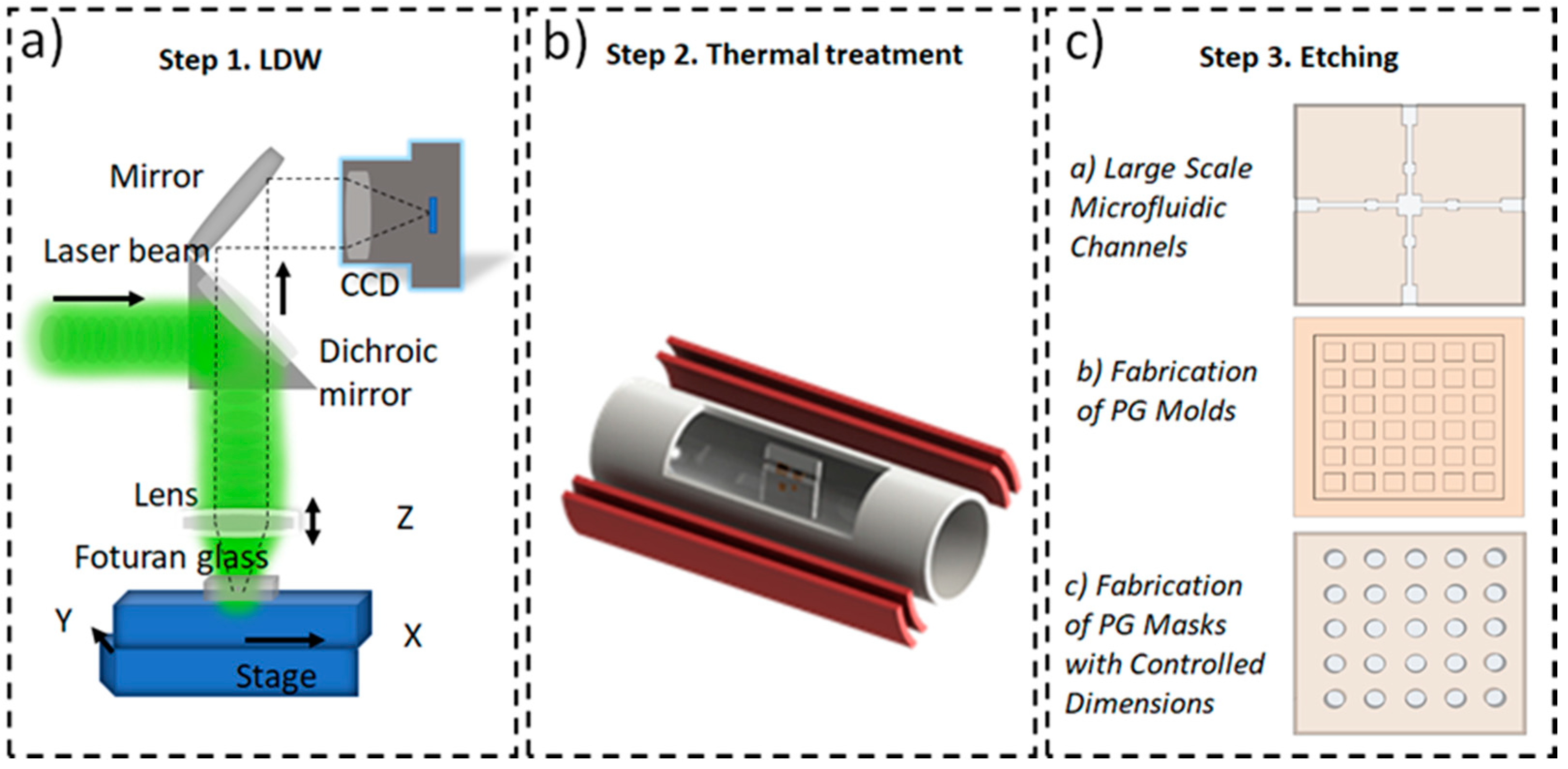
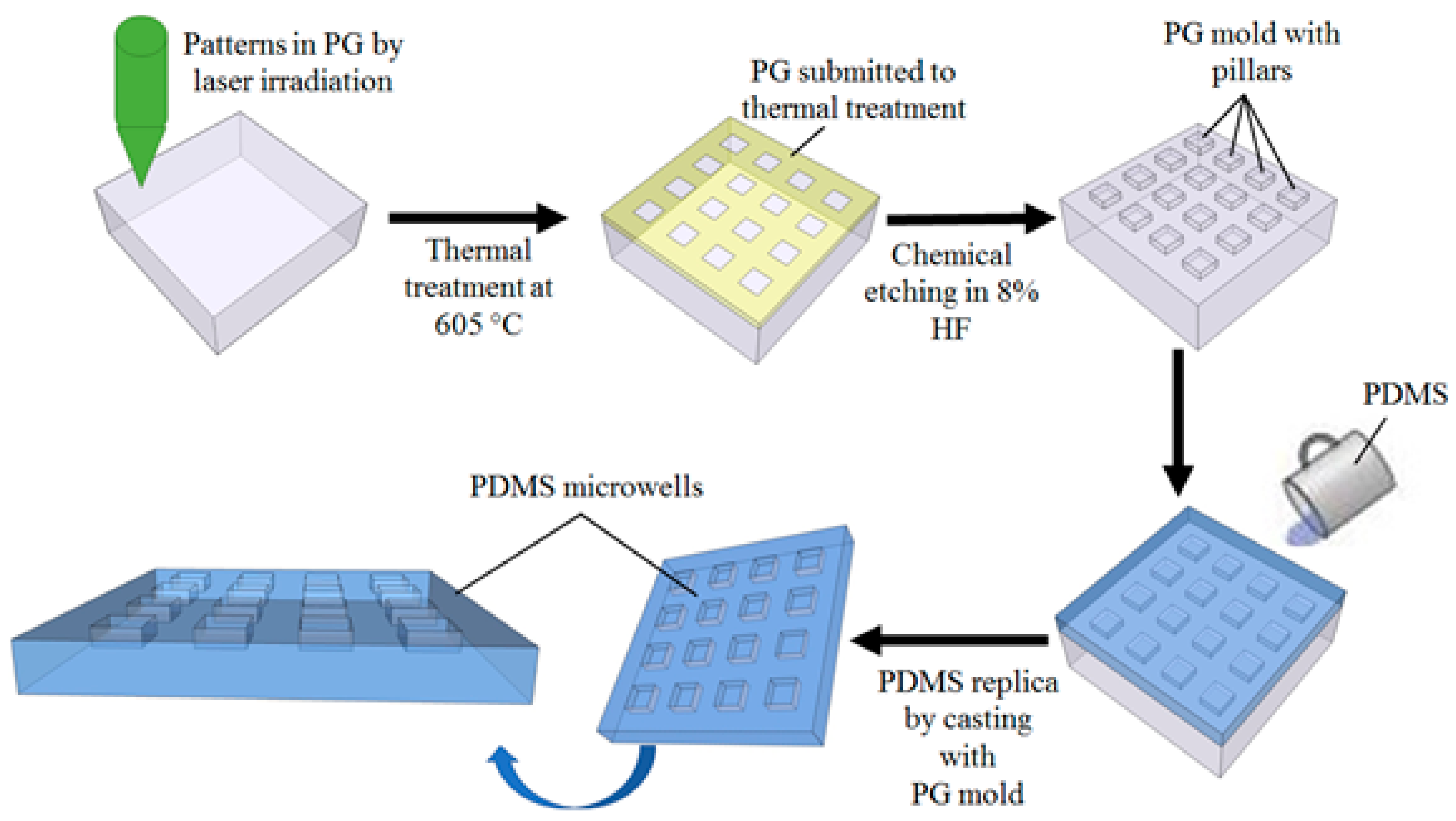
2. Materials and Methods

Laser Processing. All experiments were performed using Foturan PG (commercially available from Schott). Foturan is a photo-structurable lithium alumino-silicate glass that accommodates small amounts of Ag2O (0.05–0.15%) and Ce2O3 (0.01–0.04%), primarily designed for the UV light-induced selective microstructuring.
The protocol for obtaining free-form shaped microstructures in Foturan glass using PLAE is schematically depicted in Figure 1. LDW was carried out using a ps laser source (Coherent, model Lumera HyperRapid 50), delivering pulses of about 10-ps duration at 500-kHz repetition rate. The large-scale area microfluidic structures and PG molds were fabricated using visible (VIS—532 nm) ps laser, which proved to be more appropriate for a precise and controlled volume processing, while UV (355 nm) laser pulses were employed for fabrication of photo-masks, since it was experimentally found that the ps laser was more adequate for efficient and rapid formation of through-holes in bulk glass. Laser power was adjusted between 30–50 mW in case of UV and 500–600 mW for VIS laser pulses. The laser beam was focused onto the sample surface using an aspheric lens of 15-mm focal length and 0.5 numerical aperture to generate a circular spot of about 4 µm in diameter (calculated by w = 2fλM2/πD, where w is the minimum beam waist radius, f is a focal distance of the focusing lens, M is a quality beam factor, D is a laser beam diameter, and λ is the wavelength of the laser used [43]). The writing speed was varied from 0.1 to 1 mm/s depending on the pattern dimensions and geometrical features. The samples were placed on a customized LDW processing platform consisting of motorized translation stages (PlanarDL Aerotech), providing a spatial resolution of a few tens of nanometers (Figure 1a). The experiments were carried out in a clean room, in air, at atmospheric pressure, and were in-situ monitored with a charge-coupled device (CCD) camera (Thorlabs).
In a subsequent step (Figure 1b), the laser-exposed glass samples were annealed in a programmable furnace (Carbolite, model MTF M1238-250). First, controlled heating with a slope of 5 °C/min up to 500 °C was performed. Then the temperature was kept constant for 1 h in order to cause diffusion of precipitated Ag atoms to grow Ag nanoclusters. Next, the temperature was increased again with a slope of 3 °C/min up to 605 °C and kept constant for another hour to induce the formation of crystalline lithium metasilicate phase around the grown Ag nanoclusters, which acted as nuclei. The latent image formed during the laser direct writing process was then developed by the thermal treatment to be visible. By changing the laser fluence and scanning speed one may thus modify the glass and evaluate tracing line thicknesses (Figure 2). The pulse overlap for all cases can be estimated to more than 99.9%. This evaluation allows choosing further laser parameters for the glass processing for specific needs, e.g., thinner lines for higher-resolution processing or thicker lines for larger-area modification. In our case we found threshold line widths of about 4 μm in case of UV laser pulses and of 5.5 μm in case of VIS, which can increase with increasing laser fluence and decreasing scanning speed (Figure 2b,d).
In the last step, the glass samples were submitted to chemical etching in an 8% HF solution under the ultrasonic condition (Figure 1c). During the wet etching process, the grown crystalline phase was selectively removed, since it had higher etching rate as compared with laser-unexposed regions [18] Microstructures corresponding to the laser written trajectory were then produced in Foturan glass. The second annealing treatment at 635 °C was further employed for surface smoothening.
MAPLE processing: MAPLE experiments were performed inside a stainless-steel reaction chamber. An UV KrF* excimer laser source (Lambda Physics Coherent, COMPexPro 205) delivering pulses at a wavelength of λ = 248 nm, with a duration of τFWHM = 25 ns (FWHM-Full Width at Half Maximum), and operated at a repetition rate of 5 Hz was used for thin film deposition through PG masks. In one experiment, a cryogenic target consisting of organic carbon precursors (phloroglucinol/glyoxylic acid and the template Pluronic F127 dissolved in a chloroform/ethanol mixture) was frozen in liquid nitrogen. Three thousand pulses of 4 J cm−2 incident laser fluence were subsequently applied in a dynamic pressure of ~5 × 10⁻² mbar for deposition. In another experiment we used a target prepared by immersing an aqueous solution containing graphene oxide nanocolloids (GON, 2 mg/mL Sigma Aldrich) in liquid nitrogen. We applied 25,000 pulses of <1 J cm−2 incident laser fluence, in a dynamic pressure of ∼2 × 10² mbar for the synthesis of the micropatterns. The structures were grown on silicon substrates placed parallel to the target surface at separation distances of 4–5 cm.
The characterization of the samples was performed by optical microscopy with a transmission mode (Leica, model DM4000 B Led). Scanning electron microscopy (SEM) investigation was carried out with an FEI Co. microscope (Inspect S model).
In vitro tests, reagents, and antibodies: Mouse monoclonal anti-vinculin antibody was purchased from Sigma-Aldrich Chemie GmbH, Taufkirchen, Germany (#V9131), and goat anti-mouse IgG-coupled Alexa Flour 594 was purchased from Invitrogen (Thermo Fisher Scientific) (#A11005). Most cell culture reagents used in this study were purchased from Gibco (Fisher Scientific UK Ltd, Loughborough, UK): Penicillin-Streptomycin (#15140-122), Dulbecco’s modified Eagle’s medium (DMEM, #21885-025), Fetal Bovine Serum (#10270-106), and Glutamax (#35050-061). Triton X-100 (#T8787) and phosphate buffered saline tablets (#P4417-100TAB) were purchased from Sigma. Bovine Serum Albumin (BSA) was from VWRTM company (#422361V) (VWR International GmbH, Wien, Austria). ProLong Diamond Antifade Mountant was purchased from Invitrogen (#P36961).
Cell culture: Primary human bone marrow-derived mesenchymal stem cells (MSC), a kind gift from the Institute of Biochemistry of Romanian Academy (Dr. Livia Sima), were used for experimental procedures in this study. They were grown in DMEM with 10% FBS (Fetal Bovine Serum), 1% Penicillin/Streptomycin (Pen-Strep) and 0.5 mM Glutamax. All cells were maintained in a humidified atmosphere at 37 °C and in the presence of 5% CO2.
Sterilization: The Foturan glass samples and coverslips were autoclaved for 30 min at 121 °C, followed by exposure to UV for 30 min prior to use for any experimental procedures.
Immunofluorescence microscopy: The surfaces of some coverslips and Foturan glass were coated with collagen (rat type I) for 30 min, followed by two times washing with PBS (Phosphate-Buffered Saline). The cells were then trypsinized and counted, and 3000 cells were seeded per sample. One hour or 24 h after seeding, cells were fixed using 1% PFA for 15 min at room temperature (RT), followed by permeabilization with 0.1% Triton X-100 for 5 min at RT. After permeabilization, the samples were blocked with 5% BSA for 1 h at RT and then incubated with primary antibody against vinculin (1:1000 dilution) in 5% BSA overnight at 4 °C. The next day, the Alexa Flour 594 conjugated secondary antibody and Alexa Fluor 488 conjugated Phalloidin were added in 5% BSA for 2 h at RT. The nuclei were stained with Hoechst in 5% BSA, 1:20,000 for 3 min at RT. After each step, PBS washes were performed three times for 5 min each. The samples were mounted using Prolong Diamond Antifade. Alternatively, for nuclei staining, we also mounted the samples by Vectashield with 4′,6-diamidino-2-phenylindole DAPI (Vector Laboratories, Burlingame, CA, USA). Images were acquired using a Leica DM4000 B LED with the 20× magnification objective.
Acquired images were processed using ImageJ software. Colocalization analysis was performed using the ImageJ JACoP plugin. The images were split into separate channels and used for threshold processing. The analysis was performed in one experiment and the total number of fields analyzed is indicated in the figure legends. The obtained values were imported into GraphPad Prism 6 software for graphical representation.
Statistical analysis: Data sets were analyzed using unpaired two-tailed Student’s t-test (with Welch correction). Mean values, SEM, and statistics were calculated with Prism6 (GraphPad software). Results with a p value less than 0.05 were considered to be significant as indicated in the figure legends. No criteria of inclusion or exclusion of data were used in this study.

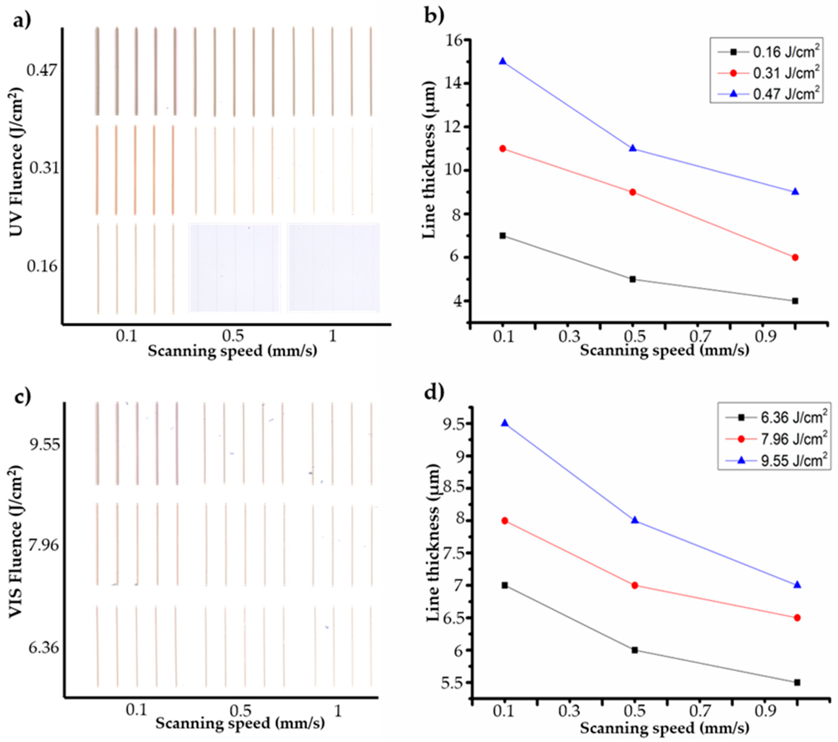
3. Results and Discussion

Ultrashort pulse laser processing of transparent Foturan glass with ps pulses was rarely addressed in the literatures. Veiko et al. [44] reported the possibility to modify Foturan glass by a ps Nd:YAG (neodymium-doped yttrium aluminum garnet (Nd:Y3Al5O12)) laser source delivering pulses of 30-ps duration at 532-nm wavelength and a repetition rate of 10 Hz. The same group showed the fabrication of 3D channels in Foturan bulk by HF etching of crystallized regions developed by annealing using a CO2 laser treatment [45].
We recently proposed the PLAE technique as an alternative to FLAE [28] by demonstrating the successful fabrication of basic 3D embedded microchannels. Ps lasers could then provide advantage over fs lasers for large-area processing of some transparent materials both on surface and in volume. Higher average power and longer pulse width can modify more volume per pulse by depositing larger energy in the material. Specifically, lower peak intensity associated with the longer pulse width allowed us to irradiate the glass with higher energy pulse without generation of damage, which increases electron density and, thus, the precipitation of more Ag atoms. The larger amount of Ag atoms was then generated, which allowed us to more efficiently develop a larger glass crystalline area by the annealing treatment. Thus, the processing times can be shortened for large-area modification as compared with fs lasers. The developed area can be finally removed by HF chemical etching. In a comparison of fabricating a comparable structure, irradiation time was approximately 1.5 h for laser pulses of 360 fs at 522 nm (2 mm/s scanning speed and 250 KHz laser repetition rate), while approximately 10 min only were necessary for 10-ps laser pulses at 532 nm (a 0.9-mm/s scanning speed and 500-KHz laser repetition rate). The shortened irradiation time for the ps laser is mostly due to the reduced number of planes scanned using line-by-line laser irradiation required to cover the desired modified volume. In the ps case, the number of planes was significantly reduced as compared with fs processing due to the larger modified volume per pulse. A more efficient process was experimentally achieved with UV pulses, since the critical dose was one order of magnitude smaller than that of VIS pulses (laser power conversion efficiencies from the fundamental beam were 1:2 for VIS and 1:3 for UV) [28].

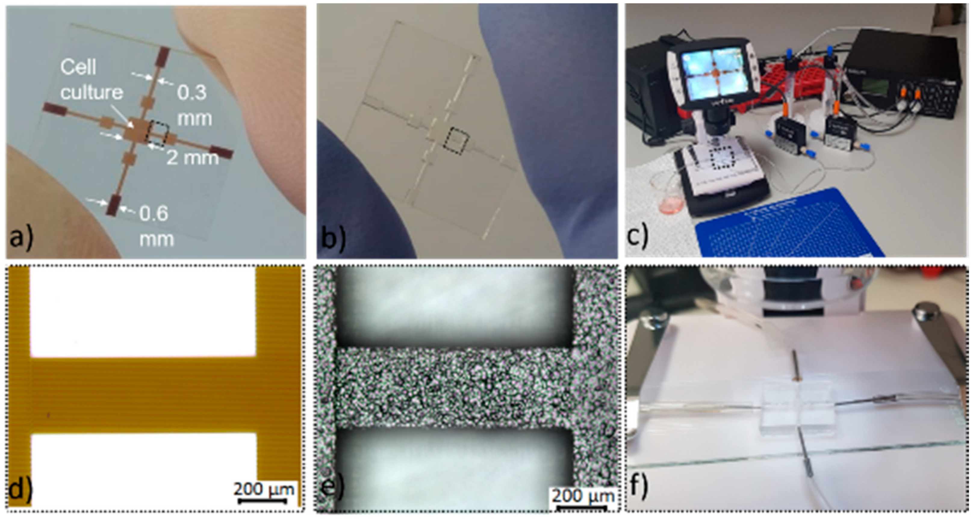
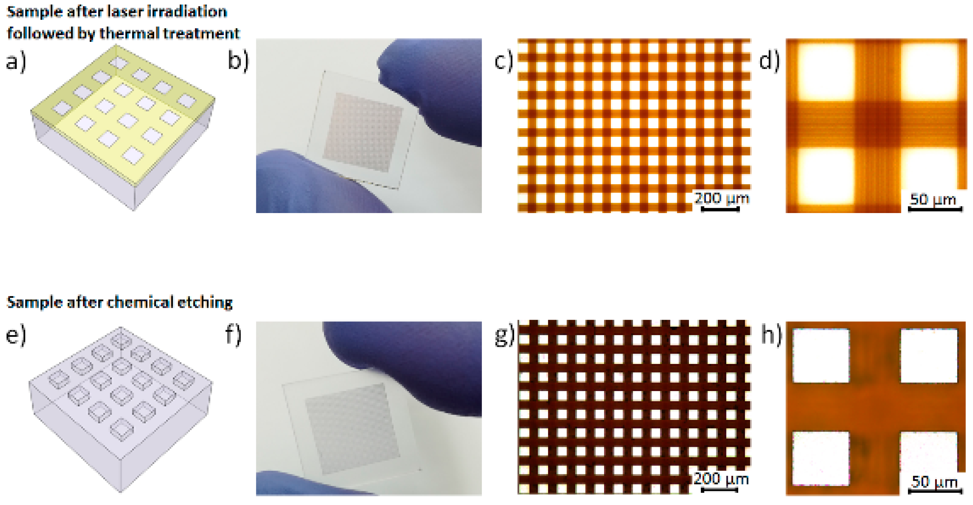
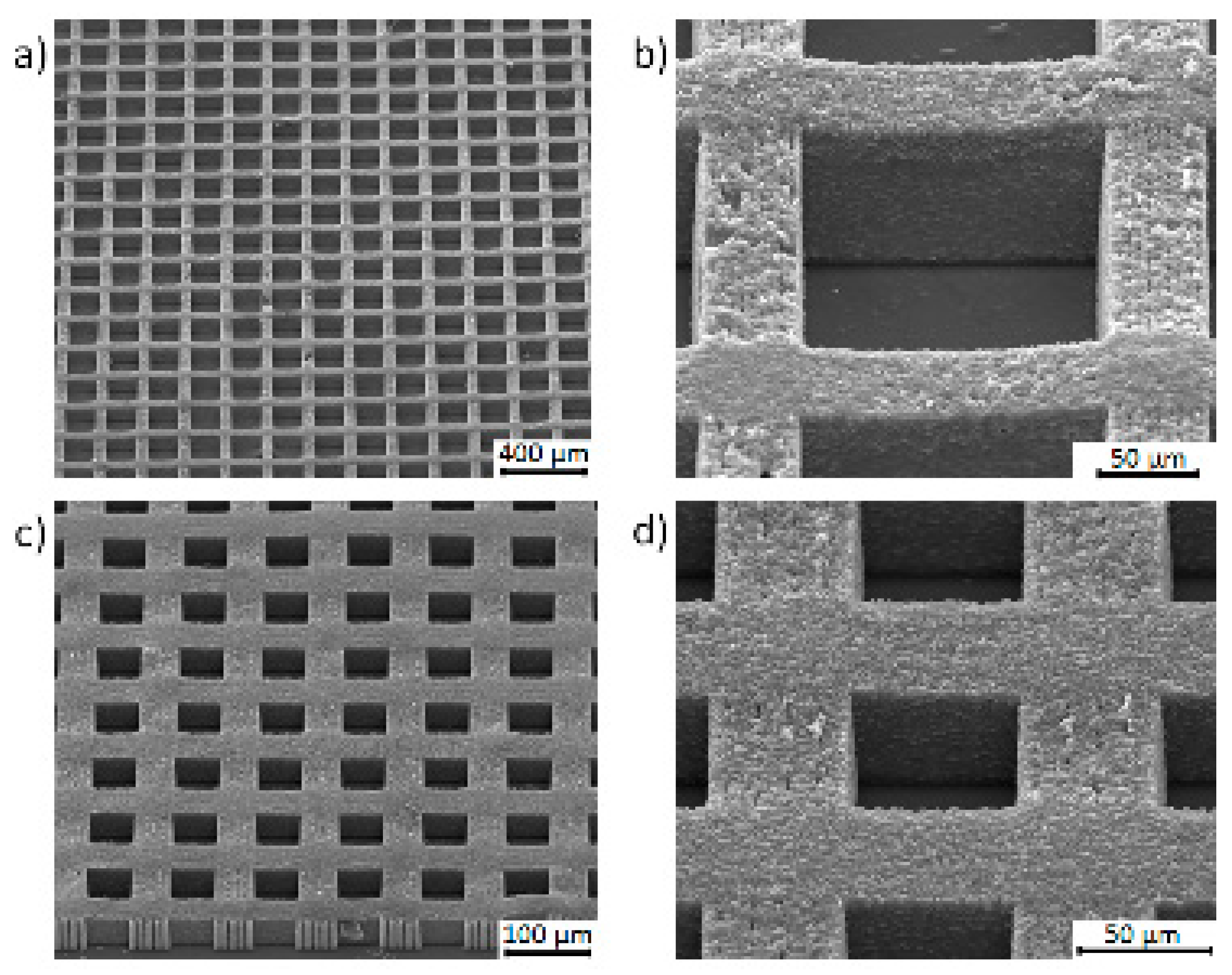
3.1. Fabrication of Large-Scale Microfluidic Channels in PG

In this section, we report on the possibility to generate complex structures on PG surfaces for fabricating open, large-scale area microfluidic devices with central cell culture chambers (Figure 3a,b). Final microfluidic chip was composed of two parts: (1) an open structure fabricated on PG surface by VIS-PLAE and (2) a PDMS sheet that sealed the fabricated structures on PG using the bounding process by activating their surfaces in oxygen plasma. The fabricated structure on PG consisted of cross-shaped microfluidic channels with microreservoirs at each end and a microchamber at the crossed region. In our design, the widths of all microfluidic channels were set to 0.3 mm while the central microchamber was 2 × 2 mm2 (Figure 3a, corresponding to a laser-irradiated sample followed by annealing treatment). It is worth to mention that the entire laser scanning process took 25 min only, at 1-mm/s scanning speed and 10-µm pitch between each scanning line. The open microstructures resulted from the selective glass removal induced by chemical etching are shown in Figure 3b. Magnified images of the microchannel parts from Figure 3a,b are presented in Figure 3d,e, respectively. Due to the limited etching selectivity in HF between the laser-irradiated and nonirradiated regions, the actual lateral dimensions of obtained structures were larger than the initially set ones, i.e., the laser-irradiated regions. The widening depended on the etching time due to the etching rate of 1-µm/minute for the nonirradiated regions. Similarly, the depth of the channel can be controlled by the etching time. For example, one can get a 10-µm-deep channel in only 1 min or a 300-µm-deep channel in half an hour by taking account of the depth of modified region and the etching selectivity between nonirradiated and irradiated regions. Even though the roughness of the channel surface was significant after the etching, the second annealing treatment can well work to reduce the roughness to nanometer scale [25]. In our design, three of the microreservoirs acted as lateral inlets and the other one, as lateral outlet, while the microchamber was used for cell culture (Figure 3c,f).
A perfusion system (Elveflow, France) was coupled to the fabricated chip using dedicated metallic connectors glued with the lateral inlets and outlets by SU-8 photoresist. The setup consisted of several elements: a pulsation-free pressure controller, flow sensors, tubing, and reservoirs dedicated to cell cultures. A detailed image of the microfluidic chip during flow monitoring is presented in Figure 3f. Thus, a 3D biomimetic microenvironment could be created in the central chamber for cell growth and visualization, which can be associated with controlled flow aspects allowing a scale up-scale down approach of the device. Indeed, the inlets were easily connected to the perfusing system while channel dimensions could be downsized to hundreds of microns (Figure 3d,e) or smaller, for specific cases. In addition, independent control can be achieved for inlet channels from 1 to 3 to mix any combination of fluids that also allows perfusion switches between different culture media or even drugs by a computer-controlled valve with sequential injection (Figure 3c,f). In a preliminary experiment we combined complete cell media (with serum), incomplete cell media (without serum), and cell media supplemented with growth factors by serial perfusing through the three inlets intermittently and monitored the response of mesenchymal stem cells (MSCs) over time.

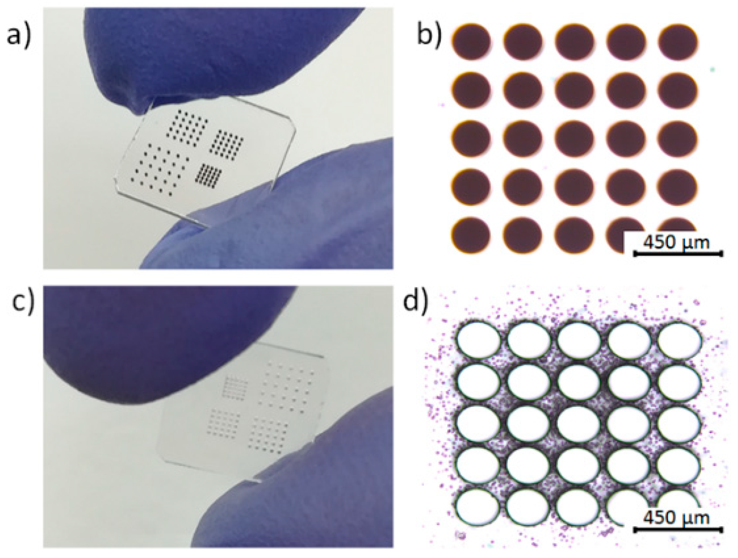
3.2. Fabrication of Myriad of Microchambers in PDMS by Using PG Molds

Studies showed that when compared with conventional methods, the use of microwell biochips in bio-nanotechnologies could result in 100- to 1000-fold reduction in the number of cells required for analyses due to great reduction of microchamber volume, down to <1 nL [7].
We advance herein the possibility to fabricate up to 10,000 microchambers in PDMS in a single step based on a PG mold processed by PLAE. The protocol is schematically depicted in Figure 4. First, we applied PLAE in order to create 3D pillars in PG after the chemical etching of laser-exposed regions. In particular, by scanning transversal lines onto PG surface, one can design a chess-like board with square dimensions tailored by the CAD (computer-aided design) program by a maskless process (Figure 5a,b). The laser-irradiated regions were designed so as to develop desired depth dimensions. Specifically, one can irradiate either with a multilayer configuration if deep channels are required or with a single-layer configuration for superficial structuring. Similarly to Section 3.1., the laser irradiation process is followed by annealing treatment at 605 °C and chemical etching in HF solution. Figure 5c,d shows the exposed PG after annealing treatment where the brown color represents modified PG and the white areas are the unmodified square structures. During the chemical etching the modified PG was selectively removed so that pillars could be created from the unmodified square regions whose heights can be controlled with the etching time. The etching rate was constant regardless of times and depths since the sufficiently deep structures were modified and the applied laser dose was kept constant within the modified structures. We, thus, obtained PG molds with 2500 pillars of 150 × 150 × 60 µm3 or even with 10,000 pillars of 50 × 50 × 30 µm3 (length × width × height). We used the fabricated PG molds to obtain replicas in PDMS, by which the pillar-prints were transcribed, i.e., microchambers with the same X-Y dimensions of glass pillars and depth corresponding to the glass pillar height. All processes are schematically shown in Figure 4.
Sketches and photographs of PG after the laser irradiation and the annealing treatment are shown in Figure 5a,b, while optical images of the exposed patterns (single-layer laser scanning) are visualized in Figure 5c,d. Similarly, Figure 5e,f depicts the mold sketch and photograph after chemical etching and Figure 5g,h presents magnified images of Figure 5f.
Using the fabricated mold, one can get controlled and efficient synthesis of thousands of microchambers having a dimension of 150 × 150 × 60 µm3 (Figure 6a). Further reduction of size to 50 × 50 × 30 µm3 is possible (Figure 6c). Tailoring the dimensions depending on target cells and/or application is then achievable. High-throughput processing of up to 104 microchambers was imprinted on 10 × 10 mm2 area (Figure 6c). The versatility of the process allowed tailoring not only the X-Y dimensions but also the pillar height by controlling PG etching time, which then reflected the microchamber depths and aspect ratios. This is shown in Figure 5g,h, in which the brown color indicates that the modified regions were not completely removed. Considering an etching rate of 10 µm/min for our experimental data, the etching times of 3 min and 6 min produced 30-µm and 60-µm depth, respectively, which were much shallower than the thickness of modified regions, of more than 200 µm. By increasing the etching time, one can increase the structure depth. Multilayer modification can create pillars higher than 200 µm with controlled lateral dimensions.

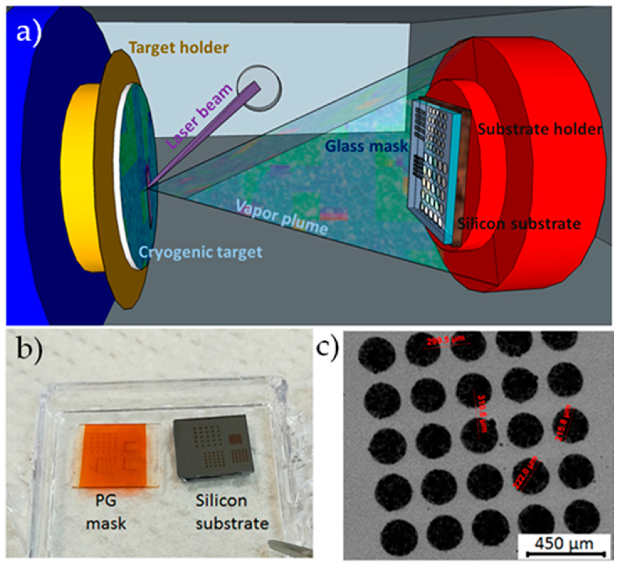
3.3. Fabrication of PG Masks with Controlled Dimensions for Additive Material Transfer

Soft lithography is the most employed technique to create micro- and nanoscale patterns on solid substrates. Although providing the best resolution, the method is expensive, time-consuming, and involves sometimes up to tens of successive steps [39]. Alternative solutions for engineering smart biofunctional surfaces reported in literatures are microcontact printing [46], dip-pen nanolithography [40], ink-jet printing [47], and laser-induced forward transfer (LIFT) [48]. Each method presents distinct advantages, while also exhibiting specific limitations.
Here we introduce the possibility to fabricate micropatterns on solid substrates by employing the mask imaging technique. We first employed PLAE to microfabricate hollow masks on PG using UV laser pulses. In this case, the main advantage of PLAE relies on the high versatility of laser direct writing of almost any kinds of shapes. A representative example of round micropatterns with 200-µm diameter, formed in PG by LDW followed by annealing, is presented in Figure 7a,b. The laser-irradiated micropatterns were constructed in volume using a lens with a 35-mm focal length and 40-mW power at an optimum scanning speed of 0.1-mm/s. This speed was precisely determined since, for slightly higher speeds, the programmed circle shape becomes elliptical. Two-layer exposure was employed by focusing the laser at 125 µm first and then 375 µm below the surface in a 500-µm-thick PG sample volume. This exposure can modify entire PG glass substrates along the z-axis so that the subsequent chemical etching treatment can create through-holes in the sample (Figure 7c,d).
In the second step, we employed additive MAPLE technique [3,49] to generate the micropatterns on silicon by transferring the evaporated material through the PG mask (Figure 8). MAPLE is a physical deposition process, typically applied for assembling delicate compounds, both organic and inorganic, on solid substrates. Detailed theoretical and experimental aspects involved in MAPLE are presented elsewhere [50]. Briefly, the procedure is based on laser evaporation of a frozen target, in which the material of interest is dissolved in a solvent. Typically, the ejected molecules are assembled on the substrate to deposit a continuous thin film, while in this case, the structured PG glass was placed in front of the substrate to generate micropatterns. As an additive process, the height of the patterns could be easily controlled by the number of the laser pulses applied for target evaporation.
In Figure 8b we show photographs of the PG mask after its use in MAPLE transfer of ejected molecules and silicon substrate on which desired patterns of materials are assembled. In this study, a mixture of organic precursors (phloroglucinol/glyoxylic acid/pluronic F127) was transferred on silicon through the PG mask, in order to generate different matrices of round micropatterns using optimized deposition conditions [51] that were shown to generate mesoporous carbon thin films. The separation distance between two adjacent micropatterns within each matrix was modified, and 100 structures were thus created in a single-step process. Graphene oxide nanomaterials (GON) were then transferred on silicon (Figure 8c), in order to generate round micropatterns of 200 µm in diameter. We tested GON because recent advances in nanomedicine revealed extensive interests for fabricating graphene-based, cell-instructive microenvironments. Target applications are related to drug/gene delivery and cancer therapy, engineering stem cell responses, bacteria-killing and tissue-engineering platforms, biosensing, and cellular imaging [52]. Melanoma cells exposed to GON-BSA coatings with compositional gradient of inhibitors were found to exhibit a dose-dependent effect on target activity [13]. Model platforms of micropatterns having predesigned shapes and sizes could be further obtained by MAPLE using PG masks with different geometrical configurations in view of creating bioinstructive structures for various assays. PG masks could be viable alternatives to conventional metal stencil masks as the former may challenge the better resolution, sharper edges, and better uniformity of geometrical shape.

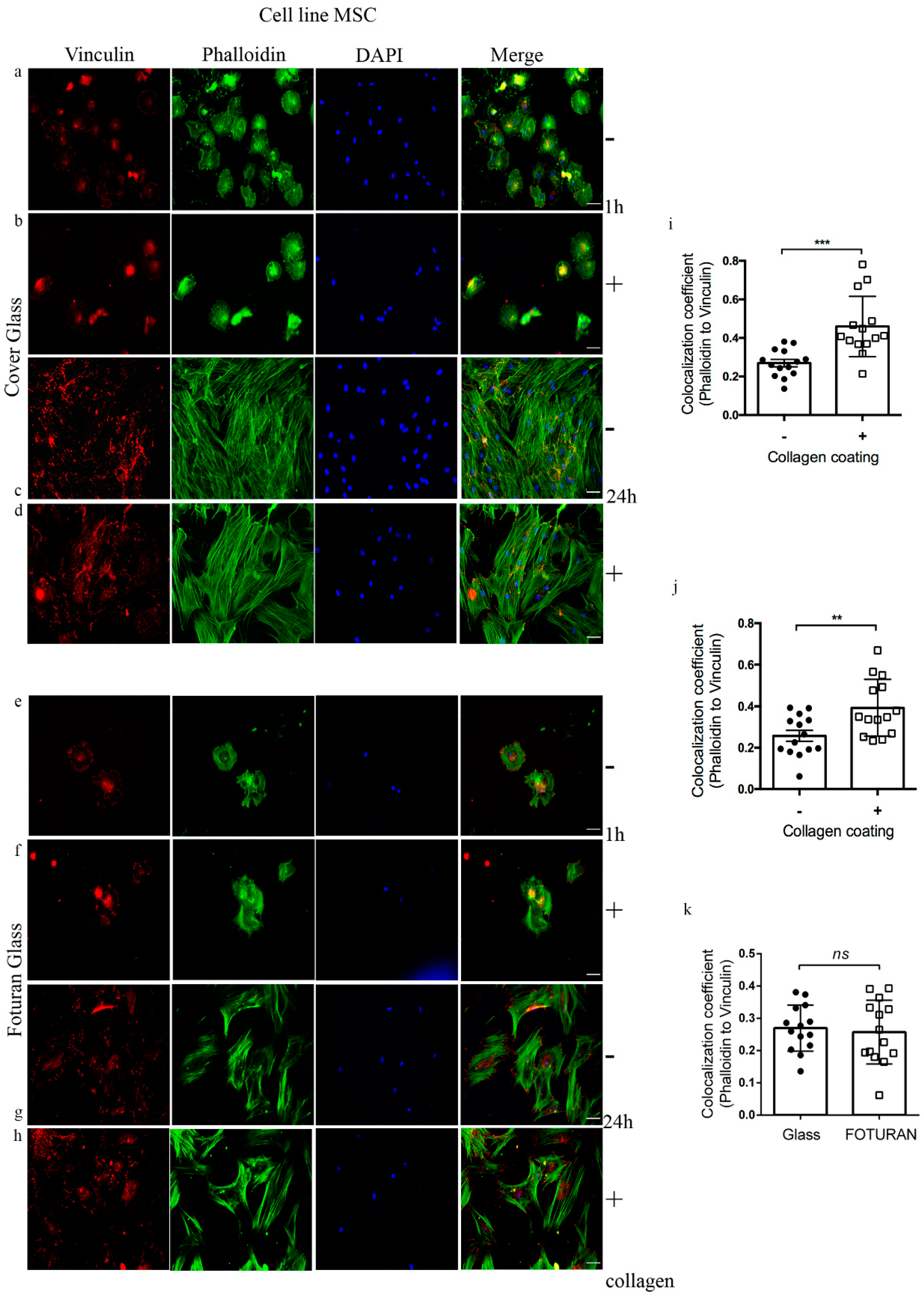
3.4. Mesenchymal Stem Cell Adhesion Studies on Laser-Processed Foturan Glass Surfaces

Cell adhesion is a biological process of fundamental importance with implications in the correct development and cell-to-cell signaling and regulation. The mechanical interaction between a cell and its extracellular matrix (ECM) can influence and control cell behavior and function. In this study we tested the laser-processed PG surfaces from the point of view of cellular adhesion. We performed immunofluorescence, staining F-actin to evidence the cytoskeleton and the focal adhesion points with vinculin since they play key roles in the cell shape control. Specifically, actin filaments and focal adhesion contacts are commonly tested structures to assess cell adhesion on certain surfaces. The fluorescent staining was employed to demonstrate that no significant morphological changes were observed when comparing the surfaces of cover glass and processed glass. Generally, cytoskeletal structure and the cellular mechanical properties are determined by the cell–matrix and cell–cell adhesions. Many cellular functions including motility and cell division depend on the response to external mechanical forces, such as extracellular matrix and neighboring cells [53]. The capacity to generate and transmit forces depends on the strength of the assembly between the integrin adhesions’ receptors and the actin-myosin cytoskeleton mediated by focal adhesion proteins (as, e.g., vinculin).
To test the biocompatibility of laser-processed PG surfaces, samples with and without collagen coating were used to analyze how cells interacted with them at two time intervals, 1 h and 24 h after seeding. The collagen coating was used, as it is known to support myogenic and osteogenic differentiation, MSCs being prone to commit to different phenotypes with extreme sensitivity to tissue-level elasticity [54]. For this purpose, we used MSCs grown on either cover glass controls or PG, bare or coated with collagen. As can be observed in Figure 9, we noticed a slight difference in the number of cells attached to the cover glass surface (Figure 9a–d), with a slight increase of the number of cells grown on the noncoated surfaces (represented by “-”, Figure 9a,c), irrespective of the time points. Although for this type of cell line, the number of attached cells is higher on bare cover glass, the collagen (represented by “+”, Figure 9b,d) still provides a better adhesion, as it can be demonstrated by quantification of the degree of actin and vinculin colocalization (Figure 9i). Same studies with MSCs grown on the laser-processed PG surfaces indicate a good biocompatibility supported by cell attachment tests (Figure 9e,f) after 1 hour and by cell adhesion assays (Figure 9g,h) after 24 h. We did not notice any difference in the number of attached cells (comparing 9e with 9f or 9g with 9h), while the increase in cell adhesion (Figure 9j) was observed when collagen was used, similarly to studies carried out on the cover glass samples. We performed the colocalization analysis to show that the laser-processed glass did not induce changes in formation of focal adhesion sites, which further played the role in mechanotransduction signaling (Figure 9k).
With all devices described above, we can foresee some critical applications to provide cell culture-specific environments easily for investigation over long time intervals. Specifically, chemotaxis-induced cancer cell migration could be achieved over extended periods in diffusion-based gradient media. The 3D reconstruction of cell migration in a chip will give information on the locomotion mechanism in tight contact with narrow spaces and would provide the means to separate the most aggressive cancer cells for further analysis. The 3D characteristics are also essential for reproducing blood vessels, mimicking capillaries in a blood–brain barrier configuration for in vitro testing of microvascular permeability and validation of an Alzheimer disease model. In addition, further analysis using a microwell 3D geometry or 2D patterns allowing single cell trapping or controlling is biologically relevant as one may be able to assess, e.g., behavior of selected cells from the same population.

4. Conclusions

PLAE technique was applied herein for the fabrication of different structures in PG and further proposed the fabricated structures for creation of biologically relevant microenvironments including: (1) large-scale area microfluidic channels for the development of a versatile perfusion system for cell culture chambers, (2) sharp-edge glass pillars for casting PDMS replica of thousands of microchambers made for single cell immobilization, and (3) PG masks with controlled geometric arrays of microholes for subsequent additive growth of biomolecules. In vitro tests evaluating mesenchymal stem cells’ behavior on the laser-processed PG surfaces demonstrated the cell viability, while a coating with collagen improved cellular adhesion. We consider PLAE an efficient alternative to FLAE for large-area laser processing and to conventional mask-based UV light exposure processes as it offers the versatility to fabricate any complex shapes either in volume or on PG surface. High repetition rate ps laser pulses allow, thus, a faster processing time and capability of developing complex surfaces and tridimensional environments with good biocompatibility at lower costs.

Author Contributions

Conceptualization, E.A., F.S., and K.S.; methodology, F.J., S.O., C.B., and M.Z.; investigation, F.J., S.O., M.Z., and E.A.; Writing, Original Draft Preparation, E.A. and F.S.; writing, review and editing, E.A., F.S., and K.S.; project administration, F.S. All authors have read and agreed to the published version of the manuscript.

Funding

This research was supported by IFA (Institute of Atomic Physics) through ELI-RO_2020_11 project, no. 01/2020 and Romanian Ministry of Education and Research, under Romanian National Nuclei Program LAPLAS VI – contract no. 16N/2019. This work has received funding from the European Union’s Horizon 2020 research and innovation program under grant agreement no. 871124 Laserlab-Europe. All authors have read and agreed to the published version of the manuscript.

Acknowledgments

The authors are grateful to Gianina Popescu-Pelin for SEM technical support.

Conflicts of Interest

The authors declare no conflict of interest.

References

  1. Sackmann, E.K.; Fulton, A.L.; Beebe, D.J. The present and future role of microfluidics in biomedical research. Nature 2014, 507, 181–189. [Google Scholar] [CrossRef] [PubMed]
  2. Francesko, A.; Cardoso, V.F.; Lanceros-Méndez, S. Lab-on-a-chip technology and microfluidics. In Microfluidics for Pharmaceutical Applications; Elsevier: Amsterdam, The Netherlands, 2019; pp. 3–36. [Google Scholar]
  3. Sima, F.; Axente, E.; Ristoscu, C.; Gallet, O.; Anselme, K.; Mihailescu, I.N. Chapter 12 “Bioresponsive surfaces and interfaces fabricated by innovative laser approaches”. In Advanced Materials Interfaces; Tiwari, A., Patra, H.K., Xang, W., Eds.; Wiley Scrivener Publishing LLC: Hoboken, NJ, USA, 2016; pp. 427–462. [Google Scholar]
  4. Tan, Y.; Tajik, A.; Chen, J.; Jia, Q.; Chowdhury, F.; Wang, L.; Chen, J.; Zhang, S.; Hong, Y.; Yi, H.; et al. Matrix softness regulates plasticity of tumour-repopulating cells via h3k9 demethylation and sox2 expression. Nat. Commun. 2014, 5, 4619. [Google Scholar] [CrossRef]
  5. Lee, J.; Abdeen, A.A.; Wycislo, K.L.; Fan, T.M.; Kilian, K.A. Interfacial geometry dictates cancer cell tumorigenicity. Nat. Mater. 2016, 15, 856. [Google Scholar] [CrossRef] [PubMed]
  6. Ma, C.; Fan, R.; Ahmad, H.; Shi, Q.; Comin-Anduix, B.; Chodon, T.; Koya, R.C.; Liu, C.-C.; Kwong, G.A.; Radu, C.G.; et al. A clinical microchip for evaluation of single immune cells reveals high functional heterogeneity in phenotypically similar t cells. Nat. Med. 2011, 17, 738. [Google Scholar] [CrossRef] [PubMed] [Green Version]
  7. Shao, N.; Qin, L. Biochips—New platforms for cell-based immunological assays. Small Methods 2018, 2, 1700254. [Google Scholar] [CrossRef] [Green Version]
  8. Li, Y.; Jang, J.H.; Wang, C.; He, B.; Zhang, K.; Zhang, P.; Vu, T.; Qin, L. Microfluidics cell loading-dock system: Ordered cellular array for dynamic lymphocyte-communication study. Adv. Biosyst. 2017, 1, 1700085. [Google Scholar] [CrossRef]
  9. Mihailescu, I.N.; Caricato, A.P. Pulsed Laser Ablation: Advances and Applications in Nanoparticles and Nanostructuring Thin Films; Pan Stanford Publishing: Singapore, 2018. [Google Scholar]
  10. Ossi, P.M.; Miotello, A.; Dinescu, M.; Geohegan, D.B. Advances in the Application of Lasers in Materials Science; Springer International Publishing Switzerland AG: Cham, Switzerland, 2018. [Google Scholar]
  11. Axente, E.; Sima, L.E.; Sima, F. Biomimetic coatings obtained by combinatorial laser technologies. Coatings 2020, 10, 463. [Google Scholar] [CrossRef]
  12. Schmidt, V.; Belegratis, M.R. Laser Technology in Biomimetics; Springer: Berlin/Heidelberg, Germany, 2016. [Google Scholar]
  13. Sima, L.E.; Chiritoiu, G.; Negut, I.; Grumezescu, V.; Orobeti, S.; Munteanu, C.V.; Sima, F.; Axente, E. Functionalized graphene oxide thin films for anti-tumor drug delivery to melanoma cells. Front. Chem. 2020, 8, 184. [Google Scholar] [CrossRef] [Green Version]
  14. Sugioka, K.; Cheng, Y. Ultrafast lasers—Reliable tools for advanced materials processing. Light Sci. Appl. 2014, 3, e149. [Google Scholar] [CrossRef]
  15. Jiang, L.J.; Maruo, S.; Osellame, R.; Xiong, W.; Campbell, J.H.; Lu, Y.F. Femtosecond laser direct writing in transparent materials based on nonlinear absorption. MRS Bull. 2016, 41, 975–983. [Google Scholar] [CrossRef]
  16. Gattass, R.R.; Mazur, E. Femtosecond laser micromachining in transparent materials. Nat. Photonics 2008, 2, 219. [Google Scholar] [CrossRef]
  17. Sugioka, K.; Cheng, Y. Femtosecond laser three-dimensional micro-and nanofabrication. Appl. Phys. Rev. 2014, 1, 041303. [Google Scholar] [CrossRef] [Green Version]
  18. Malinauskas, M.; Žukauskas, A.; Hasegawa, S.; Hayasaki, Y.; Mizeikis, V.; Buividas, R.; Juodkazis, S. Ultrafast laser processing of materials: From science to industry. Light Sci. Appl. 2016, 5, e16133. [Google Scholar] [CrossRef] [PubMed] [Green Version]
  19. Rudenko, A.; Colombier, J.-P.; Höhm, S.; Rosenfeld, A.; Krüger, J.; Bonse, J.; Itina, T.E. Spontaneous periodic ordering on the surface and in the bulk of dielectrics irradiated by ultrafast laser: A shared electromagnetic origin. Sci. Rep. 2017, 7, 12306. [Google Scholar] [CrossRef]
  20. Chanal, M.; Fedorov, V.Y.; Chambonneau, M.; Clady, R.; Tzortzakis, S.; Grojo, D. Crossing the threshold of ultrafast laser writing in bulk silicon. Nat. Commun. 2017, 8, 773. [Google Scholar] [CrossRef] [Green Version]
  21. Eaton, S.M.; Cerullo, G.; Osellame, R. Fundamentals of femtosecond laser modification of bulk dielectrics. In Femtosecond Laser Micromachining; Springer: Berlin/Heidelberg, Germany, 2012; pp. 3–18. [Google Scholar]
  22. Masuda, M.; Sugioka, K.; Cheng, Y.; Aoki, N.; Kawachi, M.; Shihoyama, K.; Toyoda, K.; Helvajian, H.; Midorikawa, K. 3-d microstructuring inside photosensitive glass by femtosecond laser excitation. Appl. Phys. A 2003, 76, 857–860. [Google Scholar] [CrossRef]
  23. Cheng, Y.; Sugioka, K.; Midorikawa, K.; Masuda, M.; Toyoda, K.; Kawachi, M.; Shihoyama, K. Three-dimensional micro-optical components embedded in photosensitive glass by a femtosecond laser. Opt. Lett. 2003, 28, 1144–1146. [Google Scholar] [CrossRef]
  24. Cheng, Y.; Sugioka, K.; Midorikawa, K.; Masuda, M.; Toyoda, K.; Kawachi, M.; Shihoyama, K. Control of the cross-sectional shape of a hollow microchannel embedded in photostructurable glass by use of a femtosecond laser. Opt. Lett. 2003, 28, 55–57. [Google Scholar] [CrossRef]
  25. Cheng, Y.; Tsai, H.-L.; Sugioka, K.; Midorikawa, K. Fabrication of 3d microoptical lenses in photosensitive glass using femtosecond laser micromachining. Appl. Phys. A 2006, 85, 11–14. [Google Scholar] [CrossRef]
  26. Wang, Z.; Sugioka, K.; Midorikawa, K. Three-dimensional integration of microoptical components buried inside photosensitive glass by femtosecond laser direct writing. Appl. Phys. A 2007, 89, 951–955. [Google Scholar] [CrossRef]
  27. Sugioka, K.; Hanada, Y.; Midorikawa, K. Three-dimensional femtosecond laser micromachining of photosensitive glass for biomicrochips. Laser Photonics Rev. 2010, 4, 386–400. [Google Scholar] [CrossRef]
  28. Jipa, F.; Iosub, S.; Calin, B.; Axente, E.; Sima, F.; Sugioka, K. High repetition rate uv versus vis picosecond laser fabrication of 3d microfluidic channels embedded in photosensitive glass. Nanomaterials 2018, 8, 583. [Google Scholar] [CrossRef] [PubMed] [Green Version]
  29. Livingston, F.; Adams, P.; Helvajian, H. Influence of cerium on the pulsed uv nanosecond laser processing of photostructurable glass ceramic materials. Appl. Surf. Sci. 2005, 247, 526–536. [Google Scholar] [CrossRef]
  30. Hanada, Y.; Sugioka, K.; Kawano, H.; Ishikawa, I.S.; Miyawaki, A.; Midorikawa, K. Nano-aquarium for dynamic observation of living cells fabricated by femtosecond laser direct writing of photostructurable glass. Biomed. Microdev. 2008, 10, 403–410. [Google Scholar] [CrossRef]
  31. Sugioka, K.; Cheng, Y. Femtosecond laser processing for optofluidic fabrication. Lab Chip 2012, 12, 3576–3589. [Google Scholar] [CrossRef]
  32. Xu, J.; Wu, D.; Hanada, Y.; Chen, C.; Wu, S.; Cheng, Y.; Sugioka, K.; Midorikawa, K. Electrofluidics fabricated by space-selective metallization in glass microfluidic structures using femtosecond laser direct writing. Lab Chip 2013, 13, 4608–4616. [Google Scholar] [CrossRef]
  33. Xu, J.; Wu, D.; Ip, J.Y.; Midorikawa, K.; Sugioka, K. Vertical sidewall electrodes monolithically integrated into 3d glass microfluidic chips using water-assisted femtosecond-laser fabrication for in situ control of electrotaxis. RSC Adv. 2015, 5, 24072–24080. [Google Scholar] [CrossRef]
  34. Bai, S.; Serien, D.; Hu, A.; Sugioka, K. 3d microfluidic surface-enhanced raman spectroscopy (sers) chips fabricated by all-femtosecond-laser-processing for real-time sensing of toxic substances. Adv. Funct. Mater. 2018, 28, 1706262. [Google Scholar] [CrossRef]
  35. Sugioka, K.; Cheng, Y.; Midorikawa, K. Three-dimensional micromachining of glass using femtosecond laser for lab-on-a-chip device manufacture. Appl. Phys. A 2005, 81, 1–10. [Google Scholar] [CrossRef]
  36. Hanada, Y.; Sugioka, K.; Shihira-Ishikawa, I.; Kawano, H.; Miyawaki, A.; Midorikawa, K. 3d microfluidic chips with integrated functional microelements fabricated by a femtosecond laser for studying the gliding mechanism of cyanobacteria. Lab Chip 2011, 11, 2109–2115. [Google Scholar] [CrossRef]
  37. Sima, F.; Kawano, H.; Hirano, M.; Miyawaki, A.; Obata, K.; Serien, D.; Sugioka, K. Mimicking intravasation–extravasation with a 3d glass nanofluidic model for the chemotaxis-free migration of cancer cells in confined spaces. Adv. Mater. Technol. 2020, 2000484. [Google Scholar] [CrossRef]
  38. Whitesides, G.M. The origins and the future of microfluidics. Nature 2006, 442, 368. [Google Scholar] [CrossRef] [PubMed]
  39. Qin, D.; Xia, Y.; Whitesides, G.M. Soft lithography for micro- and nanoscale patterning. Nat. Protoc. 2010, 5, 491. [Google Scholar] [CrossRef] [PubMed] [Green Version]
  40. Van Meer, B.; De Vries, H.; Firth, K.; van Weerd, J.; Tertoolen, L.; Karperien, H.B.J.; Jonkheijm, P.; Denning, C.; IJzerman, A.; Mummery, C.L. Small molecule absorption by pdms in the context of drug response bioassays. Biochem. Biophys. Res. Commun. 2017, 482, 323–328. [Google Scholar] [CrossRef] [PubMed] [Green Version]
  41. Song, Y.; Huang, Y.-Y.; Liu, X.; Zhang, X.; Ferrari, M.; Qin, L. Point-of-care technologies for molecular diagnostics using a drop of blood. Trends Biotechnol. 2014, 32, 132–139. [Google Scholar] [CrossRef] [Green Version]
  42. Vu, T.Q.; de Castro, R.M.B.; Qin, L. Bridging the gap: Microfluidic devices for short and long distance cell–cell communication. Lab Chip 2017, 17, 1009–1023. [Google Scholar] [CrossRef] [Green Version]
  43. Asquini, C.P. Laser induced breakdown spectroscopy (LIBS). In Handbook of Solid-State Lasers; Woodhead Publishing Limited: Cambridge, UK, 2013; pp. 551–571. [Google Scholar]
  44. Ageev, E.; Kieu, K.; Veiko, V.P. Modification of photosensitive glass-ceramic foturan by ultrashort laser pulses. In Fundamentals of Laser-Assisted Micro- and Nanotechnologies 2010; International Society for Optics and Photonics: Bellingham, WA, USA, 2011; Volume 7996, p. 79960R. [Google Scholar]
  45. Sergeev, M.; Veiko, V.; Tiguntseva, E.; Olekhnovich, R. Picosecond laser fabrication of microchannels inside foturan glass at co2 laser irradiation and following etching. Opt. Quantum Electron. 2016, 48, 485. [Google Scholar] [CrossRef]
  46. von Philipsborn, A.C.; Lang, S.; Bernard, A.; Loeschinger, J.; David, C.; Lehnert, D.; Bastmeyer, M.; Bonhoeffer, F. Microcontact printing of axon guidance molecules for generation of graded patterns. Nat. Protoc. 2006, 1, 1322. [Google Scholar] [CrossRef]
  47. Hong, S.; Zhu, J.; Mirkin, C.A. Multiple ink nanolithography: Toward a multiple-pen nano-plotter. Science 1999, 286, 523–525. [Google Scholar] [CrossRef]
  48. Piqué, A.; Serra, P. Laser Printing of Functional Materials: 3d Microfabrication, Electronics and Biomedicine; Wiley-VCH (Verlag GmbH & Co. KGaA): Weinheim, Germany, 2018. [Google Scholar]
  49. Axente, E.; Ristoscu, C.; Bigi, A.; Sima, F.; Mihailescu, I.N. Combinatorial laser synthesis of biomaterial thin films: Selection and processing for medical applications. In Advances in the Application of Lasers in Materials Science; Dinescu, M., Geohegan, D.B., Miotello, A., Ossi, P.M., Eds.; Springer International Publishing Switzerland AG: Cham, Switzerland, 2018. [Google Scholar]
  50. Sima, F.; Mihailescu, I.N. Biomimetic assemblies by matrix-assisted pulsed laser evaporation. In Laser Technology in Biomimetics; Springer: Berlin/Heidelberg, Germany, 2013; pp. 111–141. [Google Scholar]
  51. Axente, E.; Sopronyi, M.; Ghimbeu, C.M.; Nita, C.; Airoudj, A.; Schrodj, G.; Sima, F. Matrix-assisted pulsed laser evaporation: A novel approach to design mesoporous carbon films. Carbon 2017, 122, 484–495. [Google Scholar] [CrossRef]
  52. Negut, I.; Grumezescu, V.; Sima, L.E.; Axente, E. Chapter 11—Recent advances of graphene family nanomaterials for nanomedicine. In Fullerens, Graphenes and Nanotubes; Grumezescu, A.M., Ed.; William Andrew: Oxford, UK, 2018; pp. 413–455. [Google Scholar]
  53. Janmey, P.A.; Weitz, D.A. Dealing with mechanics: Mechanisms of force transduction in cells. Trends Biochem. Sci. 2004, 29, 364–370. [Google Scholar] [CrossRef] [PubMed]
  54. Engler, A.J.; Sen, S.; Sweeney, H.L.; Discher, D.E. Matrix elasticity directs stem cell lineage specification. Cell 2006, 126, 677–689. [Google Scholar] [CrossRef] [PubMed] [Green Version]
Figure 1. Schematic of the PLAE (picosecond laser-assisted etching) process: (a) laser direct writing followed by (b) thermal treatment and (c) chemical etching in HF (hydrofluoric acid).
Applsci 10 08947 g001
Figure 2. Evaluation of line widths’ function of laser fluence and scanning speed in case of UV (a,b) and VIS laser irradiation, respectively (c,d). Recorded optical images (a,c) and corresponding plotted graphs (b,d) are depicted.
Applsci 10 08947 g002
Figure 3. Microfluidic chip fabricated by PLAE in Foturan glass. Photographic images of the entire structure (a) after laser scanning and annealing, (b) after chemical etching in HF, and (c) developed chip (1.5 × 1.5 cm2) connected to perfusion system that can switch between three different reagents and provides a continuous flow; (df) detailed magnified images from the regions highlighted in dotted squares in (ac), respectively.
Applsci 10 08947 g003
Figure 4. Schematic of the fabrication procedure of the PG (photosensitive glass) mold and of 3D microchambers in PDMS. The mold was obtained after the PG processing protocol by PLAE, described in Section 2. The PDMS replica was obtained after 24 h drying at room temperature upon separating the PDMS (Polydimethylsiloxane) from the mold.
Applsci 10 08947 g004
Figure 5. Fabrication of PG glass mold. PG after laser exposure and annealing treatment: (a) sketch of the irradiated patterns; (b) photograph of the entire sample; (c) optical image of central region; (d) detailed view of (c). PG after chemical etching; (e) 3D mold sketch; (f) photograph of the entire PG mold; (g) optical image of central region; (h) detailed view of (g).
Applsci 10 08947 g005
Figure 6. SEM images of square microchambers obtained in PDMS by replication of the PG mold. (a) General view of the square microwells of 150 × 150 µm2 with 60-µm depth separated by a 50-µm thickness wall; (b) detailed view of (a); (c) general view of the square microwells of 50 × 50 µm2 with 30-µm depth separated by a 50-µm thickness wall; (d) detailed view of (c).
Applsci 10 08947 g006
Figure 7. Fabrication of PG mask with microholes. PG mask after laser exposure and annealing treatment: (a) photograph of the sample; (b) optical image of central region. PG mask after chemical etching: (c) photograph of the sample; (d) optical image of central region, PG mask with microholes.
Applsci 10 08947 g007
Figure 8. (a) Scheme of MAPLE (Matrix-Assisted Pulsed Laser Evaporation) process; (b) PG mask with microholes and silicon substrate after transfer of micropatterns; (c) SEM image of the transferred GON (Graphene Oxide Nanomaterials) micropatterns on silicon.
Applsci 10 08947 g008
Figure 9. Immunofluorescence microscopy images of MSCs (Mesenchymal Stem Cells) grown on cover glass (ad) and PG samples (similar to samples presented in Section 3.1.) developed by PLAE (eh); bare (a,c,e,g) or coated with collagen (b,d,f,h). The colocalization between phalloidin and vinculin staining, 1 h post-seeding was evaluated by calculating colocalization coefficient using JACoP (Just Another Colocalization Plugin) and the corresponding results are presented in (i), (j), and (k) (mean of n = 14 ± SEM). Two-tailed Student’s t test was used to determine the statistical significance. (** p value < 0.01, *** p value < 0.001). Scale bar is 100 μm.
Applsci 10 08947 g009
Publisher’s Note: MDPI stays neutral with regard to jurisdictional claims in published maps and institutional affiliations.

