Article

A 5.43 nV/√Hz Chopper Operational Amplifier Using Lateral PNP Input Stage with BJT Current Mirror Base Current Cancellation

Department of Electronics Engineering, Chungnam National University, Daejeon 34134, Korea
*
Author to whom correspondence should be addressed.
Appl. Sci. 2020, 10(23), 8376; https://doi.org/10.3390/app10238376
Submission received: 30 October 2020 / Revised: 22 November 2020 / Accepted: 23 November 2020 / Published: 25 November 2020
(This article belongs to the Special Issue Selected Papers from IMETI 2020)

Abstract

:
This paper presents a low-noise chopper operational amplifier using a lateral PNP input stage with bipolar junction transistor (BJT) current mirror base current cancellation. The BJT has a lower noise characteristic than the metal–oxide–semiconductor (MOS) transistor, where low-noise characteristics can be achieved by implanting the BJT to the input stage of the amplifier; however, the base current of the BJT input stage causes low input impedance of the amplifier. The BJT current mirror base current cancellation technique is implemented to enhance the input impedance of the BJT input stage by canceling the base current. BJT current mirror base current cancellation is implemented with a simple scheme using NPN transistors with deep n-well in a generic complementary metal–oxide–semiconductor (CMOS) process. For further noise reduction with the BJT input stage, a chopper amplifier scheme is adopted to reduce low-frequency components such as 1/f noise terms in the low-frequency range. The prototype chip is fabricated in a 0.18-μm CMOS process. The active area of the prototype amplifier is 0.213 mm2. The measured input-referred noise is 5.43 nV/√Hz. The measured input base current of the amplifier with base current cancellation is 67.971 nA. The total amplifier current consumption is 278.3 μA, with a power supply of 3.3 V.

1. Introduction

In recent years, various products of precision amplifiers for sensor readout applications have been reported [1,2,3,4,5], e.g., low-noise characteristics essential for low speed and precision-sensing readout circuits. Low-noise techniques such as autozeroing and chopper stabilization are widely implemented in low-noise circuit designs [6,7,8,9,10]. Autozeroing can achieve a low-noise characteristic; however, the noise level is limited by the high-frequency noise-folding. The chopper stabilization technique can also achieve a low-noise characteristic; however, ripples caused by modulated low-frequency noises occur, and a large low-pass filter (LPF) is needed to reject those ripples. The multipath amplifier scheme with chopper stabilization is suitable for precision-sensing, achieving low-noise and low-offset characteristics with a wide bandwidth [11,12,13,14]. The multipath amplifier scheme, however, has high circuit complexity, causing difficulties in circuit design.
Bipolar junction transistors (BJTs) can be implemented in the input stage of the amplifier for achieving lower noise characteristics than metal–oxide–semiconductor (MOS) transistors [15]. The implementation of BJTs in a complementary metal–oxide–semiconductor (CMOS) process has been reported in previous works [16,17,18,19,20,21]. The implementation of a BJT into the input stage of an amplifier can achieve a low-noise characteristic; however, the biggest disadvantage of BJTs in the input stage of the amplifier is the low input impedance caused by the large input bias current caused by the base current [20].
In this paper, a low-noise chopper operational amplifier using a lateral PNP input stage with BJT current mirror base current cancellation is presented. The input stage of the amplifier is implemented with a custom-designed lateral PNP in a standard 0.18-μm CMOS process. The BJT current mirror base current cancellation scheme is implemented to cancel the base current and enhance input impedance. The BJT current mirror base current cancellation scheme is implemented with a simple scheme using NPN transistors with deep n-well. The chopper amplifier scheme is implemented for further noise reduction with the BJT input stage in the low-frequency range by reducing low-frequency components such as 1/f noise terms.

2. Circuit Implementation

The overall noise of an amplifier is majorly caused by the input differential pair, which means that the input transistors of the differential pair are the noise source of the amplifier. As shown in previous works, the BJT has a better low-noise characteristic than the MOS transistor when the same amount of bias current is supplied [15]. Vertical BJTs are supported by the process design kit (PDK) in a standard CMOS process. The supported vertical PNP of the standard CMOS process, however, has a limitation—for implementing to the input stage of the amplifier, the collector is tied with the substrate, which enables its use only in such cases as bandgap reference circuits [16]. Due to this limitation of the vertical BJT in circuit design, a lateral BJT is designed and implemented in this work. The input differential pair is implemented with lateral PNP in this work. The implemented lateral PNP is shown in Figure 1. The top view and cross-sectional view of the implemented lateral PNP are shown in Figure 1a,b. The lateral PNP is designed in a standard 0.18-μm CMOS process. The custom lateral PNP is designed with minimum length, satisfying the design rule of the standard 0.18-μm CMOS process. The lateral PNP is designed as a gated PNP, which is formed by gate polysilicon. The lateral PNP in this work is based on previously reported works [18,19,20,21]. The gate of the design lateral PNP is biased with a supply voltage of 3.3 V. The measured current gain (β) dependence on the voltage across the base and emitter (VBE) of the implemented lateral PNP is shown in Figure 1c. The β dependence on VBE shows the trend of β by the voltage sweep of VBE across 0.4 to 1.0 V. The measured maximum β is 9.3. The low β is caused by the large base current, which causes a low input impedance of the amplifier.
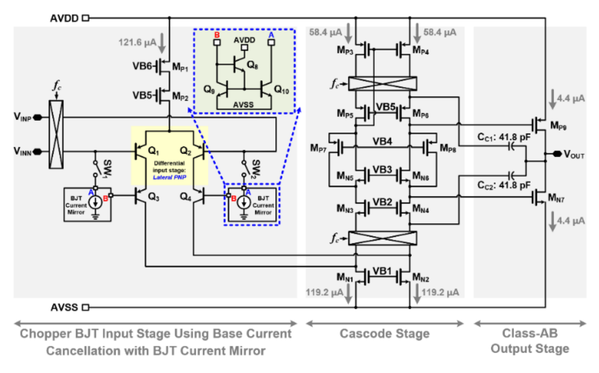
The proposed low-noise chopper operational amplifier using a lateral PNP input stage with BJT current mirror base current cancellation is shown in Figure 2. The input stage of the amplifier is implemented with a custom-designed lateral PNP. The base current caused by the lateral PNP differential input leads to low input impedance. The BJT current mirror base current cancellation scheme is implemented to reduce the base current caused by the lateral PNP input stage. The base current cancellation control switches (SW1 and SW2) are integrated for controlling the base current cancellation. The proposed chopper amplifier is adopted with a folded cascode and a class-AB output stage. The integrated compensation capacitors CC1 and CC2 are 41.8 pF. The chopper clock signals are nonoverlapping clocks, and the chopper frequency (fc) is 250 kHz.
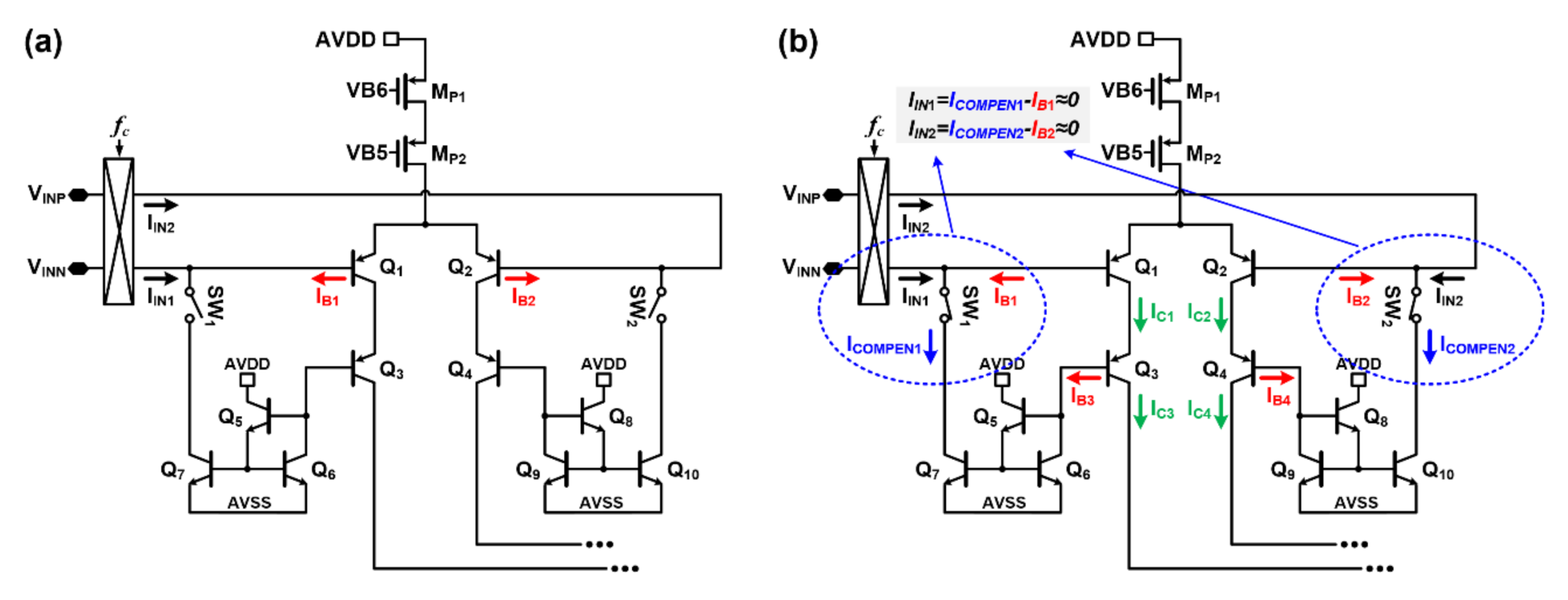
The operation of the proposed BJT current mirror base current cancellation is shown in Figure 3. The BJT current mirror base current cancellation is implemented with a simple scheme using NPN transistors with deep n-well in a generic CMOS process. The base current flow before the base current cancellation operation is shown in Figure 3a. The output base currents IB1 and IB2 of the differential input pair Q1 and Q2 cause input bias currents IIN1 and IIN2. The operation of the proposed BJT current mirror base current cancellation is shown in Figure 3b. The base current cancellation operates when the control switches SW1 and SW2 are turned on. The base currents IB1 and IB2 of the differential input pair Q1 and Q2 can be compensated by the base current cancellation. The collector currents IC1 and IC2 generated by Q1 and Q2 flow through PNP transistors Q3 and Q4. The collector currents IC1 and IC2 are the same as IC3 and IC4 of Q3 and Q4, which can be expressed as (1) and (2).
I C 1 = I C 3
I C 2 = I C 4
The PNP transistors Q3 and Q4 copy and generate the same base currents as Q1 and Q2 by the collector currents IC3 and IC4 flowing through them. The generated base currents IB3 and IB4 are the same as the base currents IB1 and IB2 of input PNP transistors Q1 and Q2 as (3) and (4).
I B 1 = I B 3
I B 2 = I B 4
The generated base currents IB3 and IB4 of Q3 and Q4 are mirrored by the BJT current mirror generating ICOMPEN1 and ICOMPEN2 for base current compensation, which can be expressed as (5) and (6).
I B 3 = I C O M P E N 1
I B 4 = I C O M P E N 2
The input bias currents IIN1 and IIN2 are compensated by the compensation currents ICOMPEN1 and ICOMPEN2 by the proposed BJT current mirror base current cancellation, and the input bias currents IIN1 and IIN2 are ideally zero by the proposed compensation circuits. The input bias currents IIN1 and IIN2 compensated by base current compensation can be expressed as (7) and (8).
I I N 1 = I C O M P E N 1 I B 1
I I N 2 = I C O M P E N 2 I B 2

3. Measurement Results

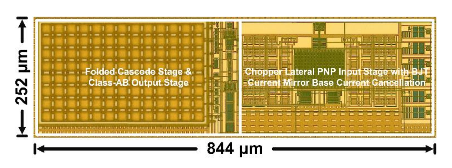
The die photograph of the fabricated low-noise chopper operational amplifier is shown in Figure 4. The prototype chopper operational amplifier is fabricated by a 0.18-μm CMOS process. The prototype chip has an amplifier-active area of 0.213 mm2. The measured total current consumption of the chopper operational amplifier is 278.3 μA, with a power supply of 3.3 V.
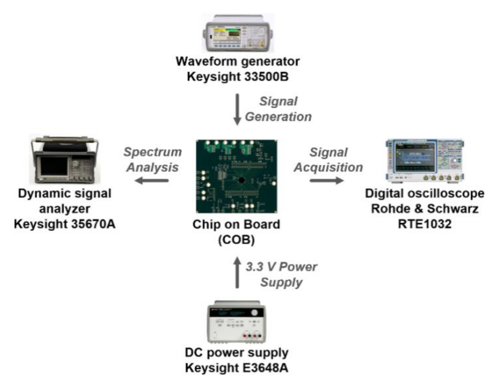
The measurement environment of the prototype chopper operational amplifier is shown in Figure 5. The prototype amplifier is tested on a designed printed circuit board (PCB) by a chip-on-board process (COB) connected by wire bonding. The DC power supply supplies 3.3 V of power, and the gate of the lateral PNP input stage is biased with 3.3 V. The waveform generator generates input pulses and sinusoidal signals for amplifier configuration tests. The dynamic signal analyzer is used for spectrum analysis, and a digital oscilloscope is used for signal acquisition.
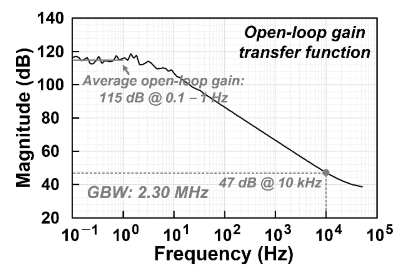
The open-loop gain measurement result of the proposed chopper operational amplifier is shown in Figure 6. The measured average open-loop gain is 115 dB, and the measured gain bandwidth (GBW) of the chopper operational amplifier is 2.30 MHz, with a chopper frequency of 250 kHz.
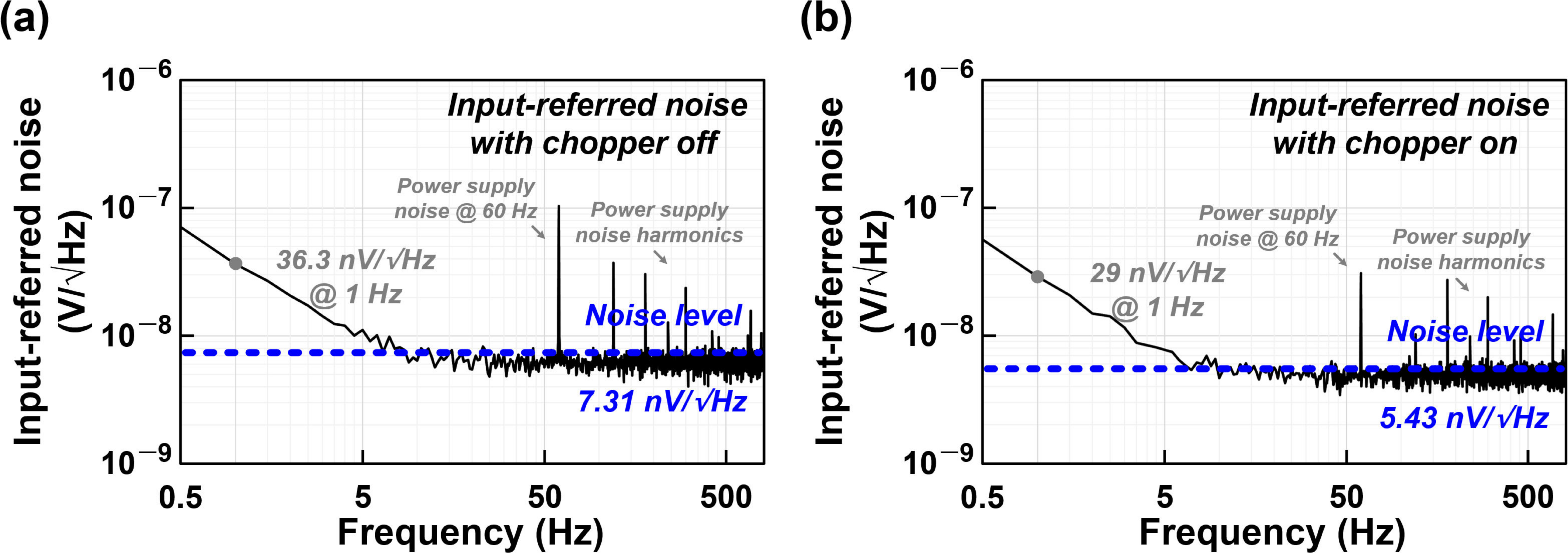
The measurement results of the input-referred noise are shown in Figure 7. The measured input-referred noise with the chopper off is shown in Figure 7a. The measured input-referred noise, with the chopper off at 1 Hz, is 36.3 nV/√Hz. The measured input-referred noise level with the chopper off is 7.31 nV/√Hz, with a noise-integrated bandwidth of 0.5 to 800 Hz. The measured input-referred noise with the chopper on, with a chopper frequency of 250 kHz, is shown in Figure 7b. The measured input-referred noise, with the chopper on at 1 Hz, is 29 nV/√Hz. The measured input-referred noise level with the chopper on is 5.43 nV/√Hz, with a noise-integrated bandwidth of 0.5 to 800 Hz. The measurement results show that the implementation of the BJT input stage can achieve a low-noise characteristic compared to previous works [13,14,22]. The measurement results, with the chopper off and on, show that the overall noise characteristic can be improved by using the chopper.
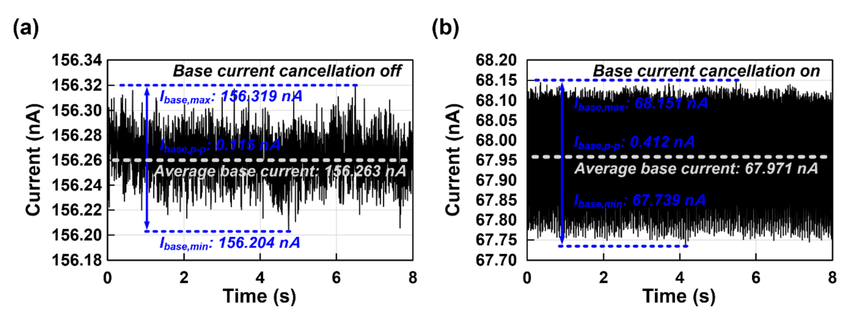
The measurement results of the input base current, with a chopper frequency of 250 kHz, are shown in Figure 8. The measured input base current without the proposed base current cancellation is 156.263 nA, which is shown in Figure 8a. The measured input base current with the proposed base current cancellation is 67.971 nA, which is shown in Figure 8b. The measurement results show that the proposed base current cancellation does not completely cancel the input base current; however, the input base current can be compensated by reducing the input base current by more than half of that before the base current cancellation operation.
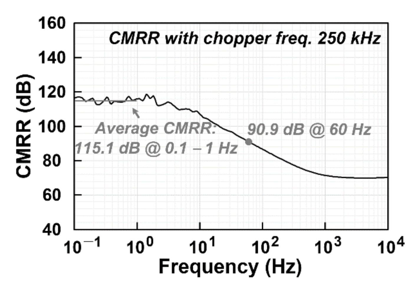
The common mode rejection ratio (CMRR) measurement result of the proposed chopper operational amplifier is shown in Figure 9. The measured average CMRR is 115.1 dB, and CMRR at 60 Hz is 90.9 dB with a chopper frequency of 250 kHz.
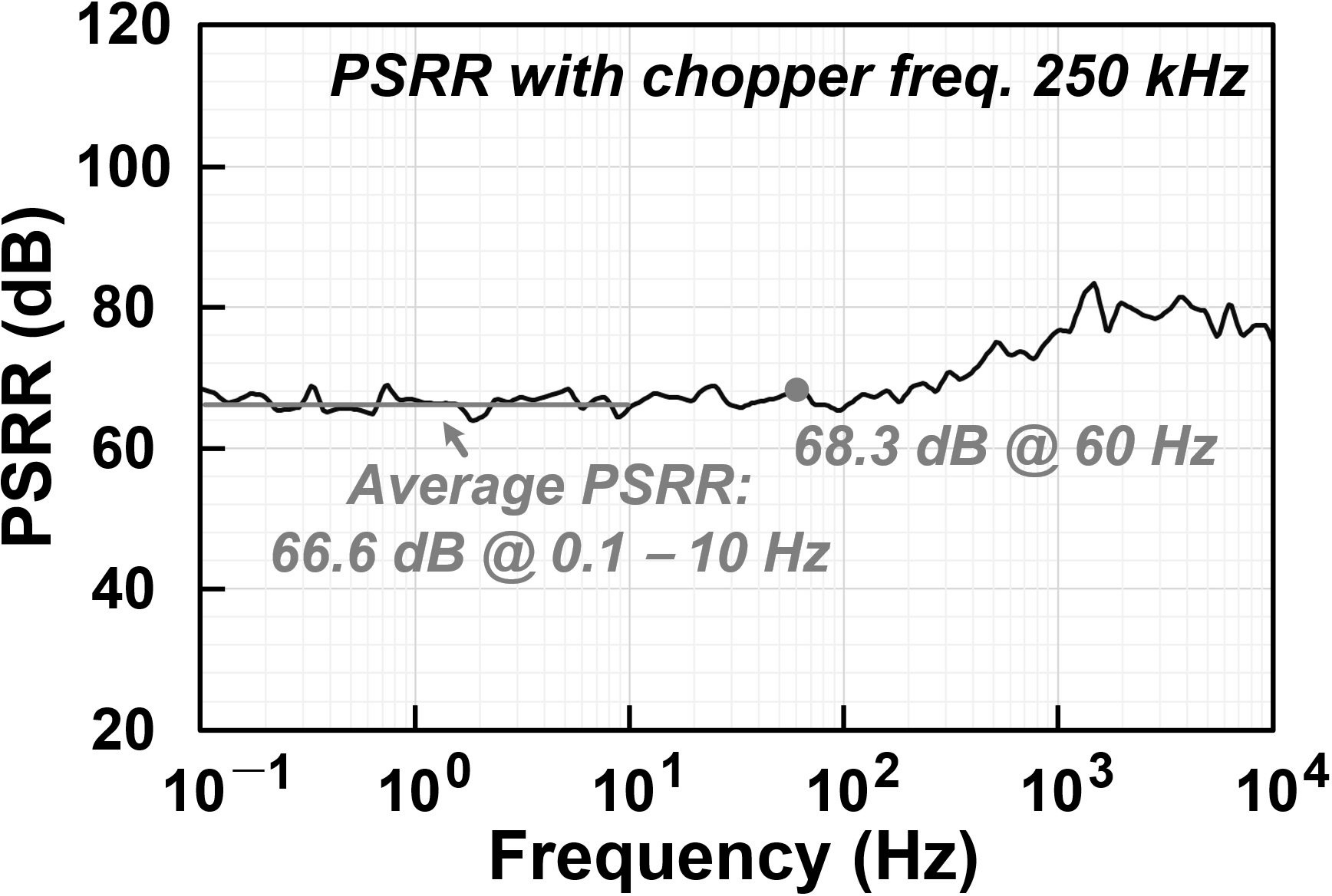
The power supply rejection ratio (PSRR) measurement result of the proposed chopper operational amplifier is shown in Figure 10. The measured average PSRR is 66.6 dB, and PSRR at 60 Hz is 68.3dB with a chopper frequency of 250 kHz.
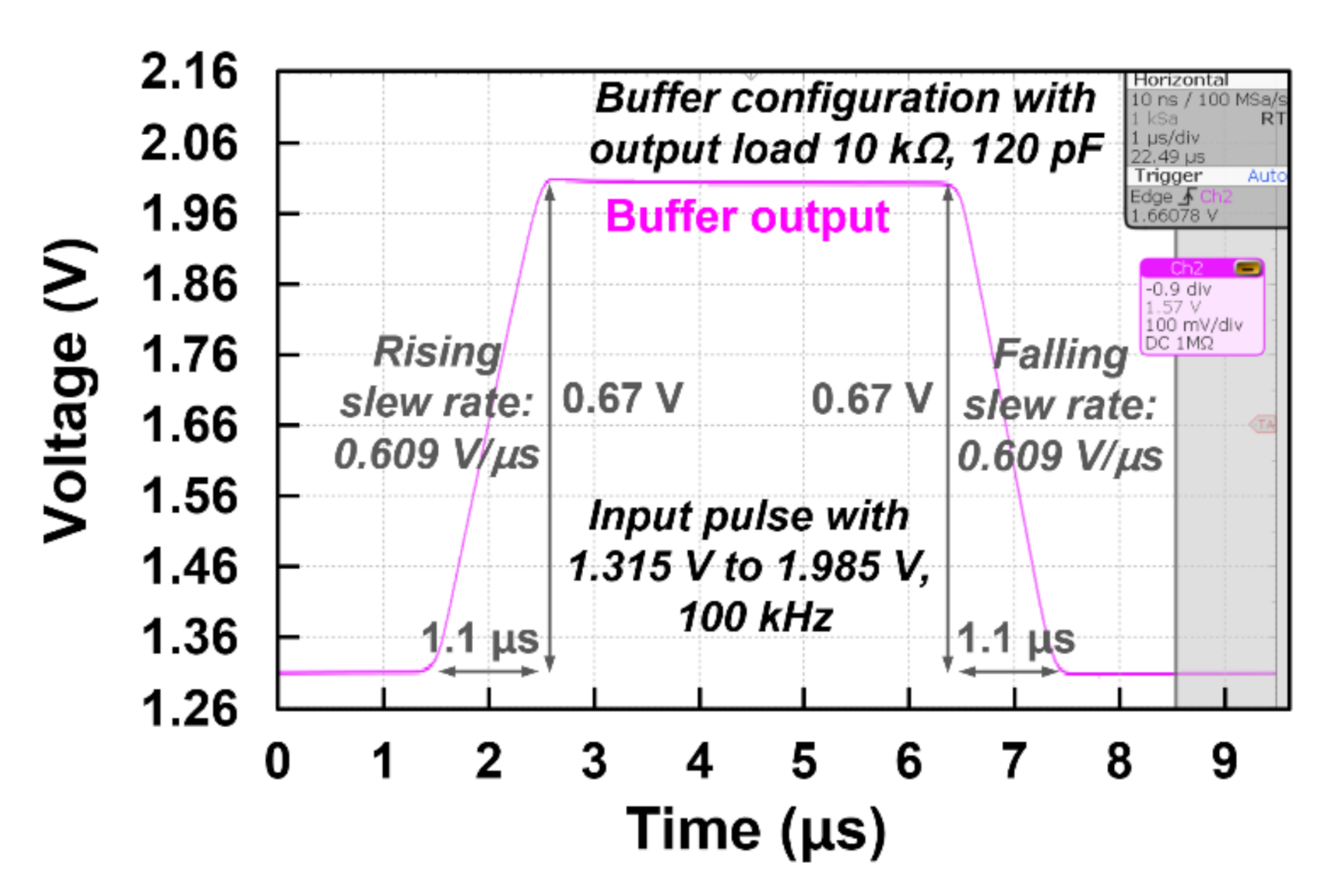
The slew rate measurement result is shown in Figure 11. The slew rate measurement proceeded with a buffer configuration, with a loading output load of 10 kΩ and 120 pF. The input voltage signal is given, with a range of 1.315 V to 1.985 V and a frequency of 100 kHz. The measured rising and falling slew rates are each 0.609 V/μs.
The transient measurement result of the proposed chopper operational amplifier with a buffer configuration is shown in Figure 12. The buffer-transient measurement proceeded with a buffer configuration, with a loading output load of 10 kΩ and 120 pF. The input sinusoidal signal was given, with an amplitude of 250 mV and a frequency of 100 kHz. The measurement result shows that the chopper operational amplifier with a buffer configuration operates in a normal operational condition.
The transient measurement result of the proposed chopper operational amplifier with an inverting amplifier configuration is shown in Figure 13. Resistors of 5 and 10 kΩ were used for the inverting amplifier configuration, amplifying a gain of 2. The measurement result shows that the chopper operational amplifier with an inverting amplifier configuration operates in a normal operational condition.

4. Discussion

Table 1 shows a performance summary and comparison with previously reported works. The noise efficiency factor (NEF) is calculated with current consumption, input-referred noise, and bandwidth for comparison of those amplifier performances [15]. The equation for calculating NEF can be expressed as Equation (9).
NEF = V rms , in · 2 · I tot π · U T · 4 kT · BW
Vrms,in is the input-referred noise, Itot is the amplifier’s total current consumption, 4kT is the thermal voltage, and BW is the amplifier bandwidth.
The NEF of the proposed amplifier is 3.98 with amplifier GBW and noise integration bandwidth of 3 MHz, which is similar and comparable to previously reported works. The measured input-referred noise of 5.43 nV/√Hz shows that the implementation of a BJT as the input of the amplifier can improve the noise performance of the amplifier.

5. Conclusions

In this paper, a low-noise chopper operational amplifier using a lateral PNP input stage with BJT current mirror base current cancellation is presented. The implementation of a BJT to the amplifier input stage can achieve improved noise performance compared to the amplifiers with a MOS transistor input stage due to the lower noise characteristic of BJTs. However, the base current of the BJT input stage causes a low input impedance of the amplifier. The proposed BJT current mirror base current cancellation, with a simple scheme, can reduce the output base current. The proposed amplifier is fabricated in a generic 0.18-μm CMOS process. The amplifier-active area is 0.213 mm2, and the total amplifier current consumption is 278.3 μA with a 3.3 V power supply. The measured input base current of the amplifier with base current cancellation was 67.971 nA, which shows that the proposed BJT current mirror base current cancellation scheme can compensate for the output base current of BJT input. The input-referred noise level is 5.43 nV/√Hz, with a NEF performance of 3.98. The proposed chopper operational amplifier achieved a low-noise characteristic and improved the input bias current using a lateral PNP input stage with BJT current mirror base current cancellation.

Author Contributions

Conceptualization and supervision, H.K. (Hyoungho Ko); investigation and writing—original draft preparation, H.K. (Hyungseup Kim); writing—review and editing, H.K. (Hyungseup Kim), Y.K., D.Y., H.-W.C., S.H.K., H.H., C.-Y.K., H.-D.L., and H.K. (Hyoungho Ko). All authors have read and agreed to the published version of the manuscript.

Funding

This work was supported by Samsung Electronics.

Acknowledgments

The EDA tool was supported by the IC Design Education Center (IDEC), Republic of Korea.

Conflicts of Interest

The authors declare no conflict of interest.

References

  1. Microchip MCP6V91. Available online: http://ww1.microchip.com/downloads/en/DeviceDoc/20005434B.pdf (accessed on 18 October 2020).
  2. Analog Devices ADA4522. Available online: https://www.analog.com/media/en/technical-documentation/data-sheets/ADA4522-1_4522-2_4522-4.pdf (accessed on 18 October 2020).
  3. Texas Instruments OPA388. Available online: https://www.ti.com/lit/ds/symlink/opa388.pdf?ts=1602963493359&ref_url=https%253A%252F%252Fwww.google.com%252F (accessed on 18 October 2020).
  4. STMicroelectronics TSZ181. Available online: https://www.st.com/resource/en/datasheet/tsz181.pdf (accessed on 18 October 2020).
  5. On Semiconductor AND9857. Available online: https://www.onsemi.com/pub/Collateral/AND9857-D.PDF (accessed on 18 October 2020).
  6. Enz, C.C.; Temes, G.C. Circuit techniques for reducing the effects of op-amp imperfections: Autozeroing, correlated double sampling, and chopper stabilization. Proc. IEEE 1996, 84, 1584–1614. [Google Scholar] [CrossRef] [Green Version]
  7. Opris, I.E.; Kovacs, G.T.A. A rail-to-rail ping-pong op-amp. IEEE J. Solid-State Circuits 1996, 31, 1320–1324. [Google Scholar] [CrossRef]
  8. Oliaei, O. Noise analysis of correlated double sampling SC integrators with a hold capacitor. IEEE Trans. Circuits Syst. I Fundam. Theory Appl. 2003, 50, 1198–1202. [Google Scholar] [CrossRef]
  9. Bakker, A.; Thiele, K.; Huijsing, J.H. A CMOS nested-chopper instrumentation amplifier with 100-nV offset. IEEE J. Solid-State Circuits 2000, 35, 1877–1883. [Google Scholar] [CrossRef]
  10. Lee, C.; Song, J. A chopper stabilized current-feedback instrumentation amplifier for EEG acquisition applications. IEEE Access 2019, 7, 11565–11569. [Google Scholar] [CrossRef]
  11. Burt, R.; Zhang, J. A micropower chopper-stabilized operational amplifier using a SC notch filter with synchronous integration inside the continuous-time signal path. IEEE J. Solid-State Circuits 2006, 41, 2729–2736. [Google Scholar] [CrossRef]
  12. Witte, J.F.; Makinwa, K.A.A.; Huijsing, J.H. A CMOS chopper offset-stabilized opamp. IEEE J. Solid-State Circuits 2007, 42, 1529–1535. [Google Scholar] [CrossRef]
  13. Fan, Q.; Huijsing, J.H.; Makinwa, K.A.A. A 21 nV/√Hz chopper-stabilized multi-path current-feedback instrumentation amplifier with 2 μV offset. IEEE J. Solid-State Circuits 2012, 47, 464–475. [Google Scholar] [CrossRef]
  14. Kim, J.; Kim, H.; Han, K.; You, D.; Heo, H.; Kwon, Y.; Cho, D.D.; Ko, H. Low-noise chopper-stabilized multi-path operational amplifier with nested miller compensation for high-precision sensors. Appl. Sci. 2020, 10, 281. [Google Scholar] [CrossRef] [Green Version]
  15. Steyaert, M.S.J.; Sansen, W.M.C.; Zhongyuan, C. A micropower low-noise monolithic instrumentation amplifier for medical purposes. IEEE J. Solid-State Circuits 1987, 22, 1163–1168. [Google Scholar] [CrossRef]
  16. Tsividis, Y.P.; Ulmer, R.W. A CMOS voltage references. IEEE J. Solid-State Circuits 1978, 13, 774–778. [Google Scholar] [CrossRef]
  17. Degrauwe, M.G.R.; Leuthold, O.N.; Vittoz, E.A.; Oguey, H.J.; Descombes, A. CMOS voltage references using lateral bipolar transistors. IEEE J. Solid-State Circuits 1985, 20, 1151–1157. [Google Scholar] [CrossRef]
  18. Vittoz, E.A. MOS transistors operated in the lateral bipolar mode and their application in CMOS technology. IEEE J. Solid-State Circuits 1983, 18, 273–279. [Google Scholar] [CrossRef]
  19. Pan, T.-W.; Abidi, A.A. A 50-dB variable gain amplifier using parasitic bipolar transistors in CMOS. IEEE J. Solid-State Circuits 1989, 24, 951–961. [Google Scholar] [CrossRef]
  20. Holman, W.T.; Connelly, J.A. A compact low noise operational amplifier for 1.2 µm digital CMOS technology. IEEE J. Solid-State Circuits 1995, 30, 710–714. [Google Scholar] [CrossRef]
  21. Zhao, D.; Zaman, M.F.; Ayazi, F. A chopper-stabilized lateral-BJT-input interface in 0.6µm CMOS for capacitive accelerometers. In Proceedings of the 2008 IEEE International Solid-State Circuits Conference-Digest of Technical Papers, San Francisco, CA, USA, 3–7 February 2008; pp. 584–585. [Google Scholar] [CrossRef]
  22. Kusuda, Y. A 5.9 nV/√ Hz chopper operational amplifier with 0.78 μV maximum offset and 28.3 nV/°C offset drift. In Proceedings of the 2011 IEEE International Solid-State Circuits Conference-Digest of Technical Papers, San Francisco, CA, USA, 20–24 February 2011; pp. 242–244. [Google Scholar] [CrossRef]
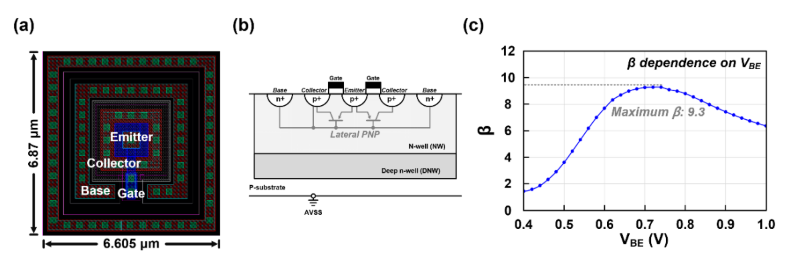
Figure 1. (a) Top view of implemented lateral PNP; (b) cross-sectional view of implemented lateral PNP; (c) measured β dependence on VBE.
Applsci 10 08376 g001
Figure 2. Schematic of low-noise chopper operational amplifier using a lateral PNP input stage with BJT current mirror base current cancellation.
Applsci 10 08376 g002
Figure 3. (a) Before base current cancellation operation; (b) operation of proposed BJT current mirror base current cancellation.
Applsci 10 08376 g003
Figure 4. Die photograph of prototype chopper operational amplifier.
Applsci 10 08376 g004
Figure 5. Measurement environment of prototype chopper operational amplifier.
Applsci 10 08376 g005
Figure 6. Open-loop gain measurement result of the proposed chopper operational amplifier.
Applsci 10 08376 g006
Figure 7. (a) Measured input-referred noise with the chopper off; (b) Measured input-referred noise with the chopper on.
Applsci 10 08376 g007
Figure 8. (a) Measured input base current without base current cancellation; (b) measured input base current with base current cancellation.
Applsci 10 08376 g008
Figure 9. Common mode rejection ratio (CMRR) measurement result of the proposed chopper operational amplifier.
Applsci 10 08376 g009
Figure 10. Power supply rejection ratio (PSRR) measurement result of the proposed chopper operational amplifier.
Applsci 10 08376 g010
Figure 11. Slew rate measurement result of the proposed chopper operational amplifier.
Applsci 10 08376 g011
Figure 12. Transient measurement result of the proposed chopper operational amplifier with a buffer configuration.
Applsci 10 08376 g012
Figure 13. Transient measurement result of the proposed chopper operational amplifier with an inverting amplifier configuration.
Applsci 10 08376 g013
Table 1. Performance summary and comparison.
This Work[14][22][13][20]
Year20202020201120101995
Process (µm)0.180.180.350.71.2
Input stage transistorBJTMOS transistorMOS transistorMOS transistorBJT
Amplifier schemeChopper amplifierMultipath amplifierMultipath amplifierMultipath amplifier2-stage amplifier
Supply voltage (V)3.31.82.5–5.55±2.5
Current consumption (µA)278.396.71470 1432100
DC gain (dB)115>137>150-20.8
(closed loop)
BW (MHz)2.303.1641.8122
Input referred noise (nV/√Hz)5.4311.85.910.53.2
Input bias current (nA)67.971-0.072<0.2501680
CMRR (dB)90.9>125>15013799.6
PSRR (dB)68.3>100>15012067.6
Area (mm2)0.2131.181.261.80.211
NEF3.98 *4.468.44.85.64
* Noise efficiency factor (NEF) with measured gain bandwidth (GBW) and noise integration bandwidth (BW) of 3 MHz.
Publisher’s Note: MDPI stays neutral with regard to jurisdictional claims in published maps and institutional affiliations.