1. Introduction
Most of the conventional renewable energy storage system is made up of multiple converters [
1] with at least one for storage and another for supply. The essential power conversion circuits lead to cost and size increase. The introduction of a bidirectional converter [
2,
3] with bidirectional power propagation ability can effectively overcome these problems and enhance the conversion efficiency.
Refs. [
4,
5,
6] are articles regarding dual active bridge (DAB) design; these circuits are featured with simple structure, easy control, and bidirectional power flow. However, there exist some problems in a single-phase shift controller, such as a narrower voltage range at light load and curtailed efficiency owing to hard switching. In the case of renewable energy regulation applications, hard switching might usually yield the current waveform to be square or sawtooth, thus invoking high-frequency electromagnetic interference (EMI) and excessive switching loss.
Resonant converters possess a soft switching feature and thus have merits of power loss reduction, with the inductor-inductor-capacitor (LLC) resonant topology being the most popular one. In charger applications, various schemes including LCC, LLC, CLLC, CLLLC, etc., have been proposed [
7,
8,
9,
10]. Owing to the advantages of soft-switching characteristic and easy control, the LCC and/or CLLC converter are popularly used in many applications. However, due to the low voltage gain in reverse operation, they are not suitable for bidirectional converter designs [
11,
12,
13]. In the bidirectional power transfer applications [
14,
15,
16], the LLC resonant converter is forced to turn into LC resonant, owing to the magnetizing inductance being clamped by the output voltage. Thus, the voltage gain is limited to be less than 1 in the backward power transfer mode, and only zero-voltage switching (ZVS) of power switches can be achieved. The lack of zero-current switching (ZCS) on the secondary rectifying devices leads to a reduction of conversion efficiency and is unsuitable for wide voltage range applications. Plus, the bidirectional LLC resonant converter is always unsymmetrical and thus results in the difficulty of a bidirectional design. Moreover, LLC only possesses the LC feature in the reverse operating mode and has limited operating range, with the voltage gain being less than 1.0. Therefore, the CLLLC design is more suitable for a bidirectional converter with wider wide operating range [
17].
An isolated type bidirectional resonant converter is developed in this paper to tackle the inherited problems faced. Compared with the bidirectional LLC resonant topology, the developed bidirectional symmetric resonant converter allows the voltage gain to be greater than 1 in the reverse mode and achieves soft switching at a full range of load as well as keeps high conversion efficiency in large power applications. Moreover, the symmetric circuit topology makes the circuit design easier and suits the bidirectional operation and wide voltage range applications.
This research principally aims at realizing a CLLLC topology, which is more suitable than LLC in accomplishing bidirectional conversion. A detailed bidirectional resonant converter design procedure is revealed, and the component parameters are derived theoretically and then validated in practice. Finally, an isolated type bidirectional resonant converter is implemented with its performance being exhibited.
2. Circuit Structure and Operation Analysis
2.1. Circuit Structure
Evolved from an LLC resonant converter, rectification diodes of the transformer secondary side are replaced by active power switches, and an inductor is introduced into the secondary side to form a resonant tank along with the resonant capacitor.
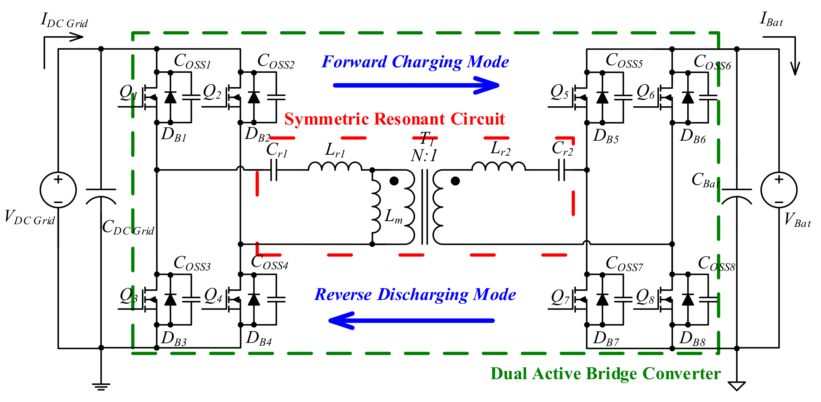
Figure 1 shows the realized topology of the isolated bidirectional symmetric resonant converter with a dual active full bridge. In definition, forward charging mode is the power transfer from power grid
VDC_Grid to battery port
VBat, and reverse discharging mode marks the power transfer reversely. With the usage of the symmetric resonant scheme, the power switches can achieve soft switching in either direction of power transfer and thus reduce the switching losses and EMI.
Figure 2 illustrates the voltage gain curves of the traditional LLC resonant converter; the reverse-mode voltage gain is limited to be less than 1.
2.2. Description of Operating Range
Figure 3 shows the voltage gain profile in the forward mode of the proposed isolated bidirectional symmetric resonant converter. It is conducted and completed by applying Mathcad and simulated software. The magnitude of voltage gain depends on the ratio of the switching frequency with respect to the resonant frequency. According to the frequency ratio, Region I only ensures ZVS. Region II ensures ZVS of power switches and ZCS of the diodes. Region III exhibits large voltage variation with only ZCS of the diodes. Therefore, Region III should be avoided for voltage control consideration [
18]. Due to the symmetric feature, the description is suitable for the reverse mode as well.
2.3. Description of Operating Range
Figure 4 shows the power propagation of the forward charging mode. The energy on the DC grid
VDC_Grid supplies energy via power switches
Q1,
Q2,
Q3, and
Q4; it passes from the transformer primary side to the secondary side and thus is rectified by the intrinsic diodes
DB5,
DB6,
DB7, and
DB8 to charge the battery
VBat. By adjusting the switching frequency, the output voltage and output power are controlled accordingly. The trigger signals of
Q1–Q4 are a pair of symmetric square waves with each being around a 50% duty ratio. With
Q1 and
Q4 being a group and
Q2 and
Q3 being another, the trigger signals of
Q1 and
Q2 are displaced by 180°, and an appropriate dead time is introduced therein. Due to the symmetric feature, the reverse discharging mode will apply the same operation. Therefore, only the forward mode operating in Region II is used to describe the operating principle.
Figure 5 illustrates the important theoretic waveforms. For simplifying the analysis, the following assumptions must be made:
The circuit operates in the steady state.
Only intrinsic diode DB and parasitic capacitance COSS are taken into account with others being ignored.
The effect of the parasitic capacitances COSS1–COSS8 is neglected.
All devices are ideal.
The output capacitances CDC_Grid and CBat are large enough to look upon VDC_Grid and VBat as the ideal voltage source.
2.3.1. Stage I [t1 < t ≤ t2]
In this stage,
Figure 6a shows that
Q1,
Q2,
Q3, and
Q4 are all cut off. At the secondary side,
DB5 and
DB8 conduct, while
DB6 and
DB7 remain cut off. At the primary side, the resonant current
iLr1 passes through
DB1 and
DB4 to keep the resonant current flow and prevent the devices from voltage spike damage. In addition, the circuit is ready for the ZVS of
Q1 and
Q4. At
t = t2, as gate signals
vGS1 and
vGS4 turn from low level to high, the next stage follows.
2.3.2. Stage II [t2 < t ≤ t3]
As shown in
Figure 6b,
Q1–Q4 remain at the cut-off state. The intrinsic diodes
DB5 and
DB8 keep on conducting while
DB6 and
DB7 remain at the cut-off state. The resonant current
iLr1 flows via intrinsic diodes
DB1 and
DB4 to retain the conduction loop. As the power switch turns on at the end at
t = t3, the ZVS is realized, whereas due to the magnetizing inductor
Lm being clamped by the output voltage
VBat and the secondary resonant capacitor voltage
VCr2, Lm is absent from resonating, and thus
iLm keeps on rising linearly. At
t = t3, resonant current
iLr1 approaches 0, and this stage ends.
2.3.3. Stage III [t3 < t ≤ t4]
As shown in
Figure 6c,
Q1 and
Q4 turn on at
t = t3 and achieve ZVS while Q
2 and Q
3 remain at the cut-off state. In this stage,
VDC_Grid passes the energy through
Cr1,
Lr1,
Cr2, and
Lr2, and it delivers the energy to the battery side via the isolated transformer. After being rectified by intrinsic diodes
DB5 and
DB8, the energy charges the battery, whereas
Lm is absent from resonating due to the magnetizing inductor
Lm being clamped by the output voltage
VBat and the secondary resonant capacitor voltage
VCr2, and thus
iLm keeps on rising linearly. At
t = t4,
iLr1 equals
iLm, and this stage terminates. In the meantime, current
iDB5,8 falls to 0, and thus ZVS is achieved.
2.3.4. Stage IV [t4 < t ≤ t5]
As shown in
Figure 6d,
Q1 and
Q4 remain conducting while
Q2 and
Q3 remain at the cut-off state. As
iLr1 equals
iLm at
t = t4, the transformer is decoupled, and electromagnetic induction takes a break. The secondary side bridge is temporarily disabled without current flow. The
DB5 and
DB8 is naturally cut off and gets ready for ZCS. In this mode, the transformer does not transfer energy to the load, and the magnetizing inductor
Lm is not clamped by the output voltage
VBat and the secondary resonant capacitor voltage
VCr2. The magnetizing inductor
Lm,
Lr1, and
Cr1 constitute a resonant circuit while
Lr2 and
Cr2 are idle. As the gating signals
vGS1 and
vGS4 turn from high to low at
t = t5,
Q1 and
Q4 cut off, and this stage ends.
2.3.5. Stage V [t5 < t ≤ t6]
As shown in
Figure 6e,
Q1 and
Q4 are cut off at
t = t5 while
Q2, Q3 still remain at the cut-off state. This exactly marks the dead time region with resonant current
iLr1 charging the parasitic capacitors
COSS1 and
COSS4 as well as helping
COSS2 and
COSS3 to discharge. In the secondary side,
DB6 and
DB7 conduct, and
DB5 and
DB8 cut off. When the voltages on
COSS2 and
COSS3 are discharged to 0 and simultaneously
COSS1 and
COSS4 are charged to
VDC_Grid, this stage terminates.
The abovementioned process from Stage I to Stage V constitutes the whole operation procedure during the positive cycle. The negative cycle has similar operating stages and thus is omitted here.
3. Equivalent Circuit and Mathematic Formulation
For obtaining the voltage gain and its relationship with respect to frequency, the fundamental harmonic approximation method (FHA) [
19] was used to build the equivalent circuit model of the forward charging mode as illustrated in
Figure 7 [
20]. Here,
VDC_Grid_FHA is the fundamental component of the square voltage waveform at the primary side.
Voe is the fundamental component of the square voltage waveform of the resonant tank and transformer. The resonant capacitance at the primary side, resonant inductance at the primary side, magnetizing inductance, resonant capacitance at the secondary side, and resonant capacitance at the secondary side are designated as
Cr1,
Lr1,
Lm,
Cr2′, and
Lr2′, respectively. Moreover, power equivalent load resistance
Roe is the AC load resistance of the energy storage battery referred to the primary side and is expressed as (1).
where
N is the transformer turn ratio, and
RBat is the equivalent resistance of battery pack. For obtaining the transfer function of voltage gain, the Laplace transform of the ratio between the output voltage and the input voltage is derived as follows.
First, the node voltage on the transformer is assigned as
vx, and based on basic circuit theory, (2) is obtained.
In (2),
Z1(s),
Z2(s),
Z3(s), and
Z4(s) are the Laplace forms of
Z1,
Z2,
Z3, and
Z4, respectively, looking from different positions, and are as expressed by (3).
By properly rearranging (2) and (3), the voltage gain function of the forward charging mode can be given as (4).
In addition, for simplifying the mathematic operation and for easily observing the gain curve, some definitions are described as follows:
fs is the switching frequency of power switches;
fr1_F is the first resonant frequency;
fn_F is the ratio of
fs and
fr1_F, referred to as normalized frequency;
Q1 represents quality factor;
k1 is the ratio of
Lm and
Lr1; g1 and
m1 represent the resonant capacitor ratio and resonant inductance ratio, respectively, with reference to the primary side. These are written as follows:
By substituting the above defined quantities into (4), it yields (8), where
Cr1 and
Lr1 are expressed as (6) and (7).
Similarly, the voltage gain of the reverse discharging mode can be derived as well. The FHA AC equivalent circuit model of reverse mode is shown in
Figure 8.
By applying the same conduction, the voltage gain transfer function of the reverse discharging mode can be expressed by (9).
where the simplified parameters
fn_R,
Q2,
k2,
g2, and
m2 are defined below.
4. The Design Procedure of Circuit Component Parameters
For meeting the performance requirements of the developed converter, some design prerequisites are listed as follows:
It must have a wide voltage range.
There must be soft switching of power switches.
Cost and size should be reduced under high frequency operation.
A good circuit design of resonant circuits is founded on selecting appropriate resonance parameters.
Figure 9 illustrates a complete design flowchart of the bidirectional symmetric resonant converter with the step-by-step design procedures being described in the following.
4.1. Step 1: Determining the Specification of Converter
Based on the circuit topology, an isolated type bidirectional symmetric resonant converter with 1 kW output power was implemented to test the validity of the conception. The specification of the converter is listed in
Table 1.
4.2. Step 2: Calculating the Transformer Turn Ratio
Following the determination of converter specifications, the proper transformer turn ratio was chosen immediately. For obtaining the flexibility of the tuning range, the transformer parameter design as expressed by (11) is based on the rated output voltage of the energy storage/supply port according to the battery nominal voltage.
4.3. Step 3: Calculating the Maximum and the Minimum Voltage Gains of Forward Mode
Step 2 determines the transformer turn ratio to be approximately at 1.2. By applying (12) and (13), the maximum and the minimum gains of the forward charging mode are obtained.
4.4. Step 4: Selecting Parameters of Q1, k1, g1, and m1 to Meet the Forward Voltage Gain Requirement
Initially, a set of proper parameter quantity was selected.
Figure 10 shows the forward voltage gain with
k1,
g1, and
m1 being fixed and the forward mode quality factor
Q1 being adjusted. It clearly shows that the voltage gain curve is not a monotonic one and
Q1 with 0.6–2 cannot realize the maximum and minimum gain requirement. Moreover, if
Q1 = 0.4, the operating range of switching frequency is too wide and will result in longer response time. Therefore, a value of
Q1 = 0.2 is suitable for the forward charging mode. With the same consideration, the selection of
k1,
g1, and
m1 is to meet the maximum and minimum gain as the primary priority.
Due to the bidirectional operation of the proposed circuit, the resonant parameters must meet the voltage regulation of both the forward and reverse charging modes. The parameter design can only be fulfilled by an iterative process. Finally, the design parameters are
Q1 = 0.2,
k1 = 3.5,
g1 = 1, and
m1 = 1, as shown in
Figure 11.
4.5. Step 5: Checking the Maximum and the Minimum Gains of the Forward Charging Mode
If the maximum and the minimum gains of the forward charging mode are not met, the design has to return to Step 4 to update the parameters Q1, k1, g1, and m1. As the conditions are met, the design can go on to the next step.
4.6. Step 6: Calculating the Resonant Device Parameters
After the quantities
Q1,
k1,
g1, and
m1 are determined, the parameters of the associated resonant devices with device parameters
Roe,
Cr1,
Lr1,
Lm,
Cr2, and
Lr2 can be obtained by (14) to (19).
4.7. Step 7: Calculating the Maximum and the Minimum Voltage Gains of Reverse Mode
According to (20) and (21), the maximum and the minimum gains of the reverse charging mode can be achieved.
4.8. Step 8: Using the Resonant Device Parameters of Step 6 to Reversely Obtain the Parameters Q2, k2, g2, and m2 of the Reverse Discharging Mode
Employing the resonant device parameters obtained from the forward charging mode and backwards, we can calculate the parameters Q2, k2, g2, and m2 of the reverse discharging mode.
4.9. Step 9: Checking the Maximum and the Minimum Gains of the Reverse Charging Mode
Mathcad is applied to examine whether the gains meet the maximum and minimum gain requirements illustrated in
Figure 12. If the gain curves of reverse charging mode cannot satisfy the maximum and minimum gains condition, we will need to return to Step 4 to readjust the amount of
Q1,
k1,
g1, and
m1 recursively until the voltage gains of both forward and backward mode meet the requirements.
4.10. Step 10: Determining the Maximum and Minimum Operating Frequencies of the Forward and Reverse Charging Modes
By inspecting
Figure 12, the maximum and minimum operating frequencies of the forward
(fs_max_Forward and
fs_min_Forward) and reverse
(fs_max_Reverse and
fs_min_Reverse) charging modes can be calculated.
4.11. Step 11: Determining the Duration of Dead Time (tdead)
The duration of dead time plays the key role of success or failure of ZVS of power switches. Too short of a dead time will lead to the unsuccessful removal of the charge on the parasitic capacitors of the power switches and yield ZVS failure while too long of a dead time would sacrifice the energy propagation time and thus increase the current stress on the primary side [
21]. Therefore, the silicon carbide (SiC) NMOS power switches C2M0160120D manufactured by the CREE Inc. with very small parasitic capacitance
COSS being equal to 55 pF are used, and thus the ZVS is easily accomplished. By using (22), the required dead time can be attained.
Because the stray capacitance and parasitic inductance are not taken into account, the dead-time interval was kept up to 200 ns for more tolerance.
5. The Structure of the Digital Signal Control System
Figure 13 shows the control system structure of the developed isolated bidirectional symmetric resonant converter. The digital signal processor (DSP) IC TMS320F28335 of Texas Instruments was employed as the control core of this bidirectional converter system to manipulate the bidirection power flow approach. In comparison with the analog scheme, the digital signal approach can effectively reduce the amount of circuit component and thus decrease the size and cost accordingly.
5.1. Control Strategy
In this research, the constant current–constant voltage control is determined as the charging strategy of battery storage. In the battery discharging mode, the constant voltage control is applied to keep the stability and reliability of the DC power grid.
Taking the battery storage as an example,
Figure 14 shows the control system block diagram of the battery storage [
22,
23], with the reference voltage signal
Vb_ref being 95% of the upper limit battery voltage and
Ib_ref being the reference current signal according to the battery charging current. When the battery is charged in the constant-current mode, the analog-to-digital converter (ADC) of the DSP will fetch the output signal
Ib and compare it with the reference current signal
Ib_ref to obtain the difference. With the compensation by a Proportional integrator (PI) controller and modulation by a frequency modulation generator (FM generator), a frequency modulated pulse-width modulation (PWM) is achieved to accomplish the constant current control.
5.2. The Step Response Test of the Charging Current
Although the constant current–constant voltage control is the charging strategy, most of the charging time is based on the constant current charging. Thus, an abrupt constant current charging fluctuation is proposed to validate the developed scheme.
Figure 15 shows the voltage and current curves under a step load current change. In
Figure 15a, the battery voltage is kept constant when load current is drastically increased, while
Figure 15b reveals that the battery voltage remains unchanged under an abrupt load current drop. It can be clearly observed that the battery voltage remains constant when load current fluctuates.
6. The Measurements and Operating Efficiency Analysis
Based on the parameters, the resonant components are calculated with Lr1 = 59.9 µH, Lr2 = 41.6 µH, Lm = 209.65 µH, Cr1 = 42.29 nF, and Cr2 = 60.9 nF. Owing to the winding transformer’s windings and resonant inductor being handmade, there definitely exists some differences from the calculated ones. Indeed, the transformer magnetizing inductance Lm was measured to be 219.85 µH, and the primary and secondly leakage inductances are Llk1 = 6 µH and Llk2 = 4 µH, respectively. Moreover, two resonant inductances are Lr1 = 55.2 µH and Lr2 = 40.36 µH. The resonant capacitors are connected in parallel; it not only can divert the current flow, but it also can reduce the current stress of each capacitor and decrease equivalent series resistance (ESR) loss with Cr1 = 41.4 nF and Cr2 = 53.7 nF.
Table 2 lists the selected parameters of the important devices in the practical circuit. The microcontroller unit (MCU) TMS320F28335 developed by TI was selected as the control core of bidirectional power flow to effectively dwindle the amount of device and reduce the size and cost. Considering the cost and the fast switching feature, the wide-band gap SiC (C2M0160120D) is used to serve the power switches (
Q1–
Q8) to promote the converter’s performance.
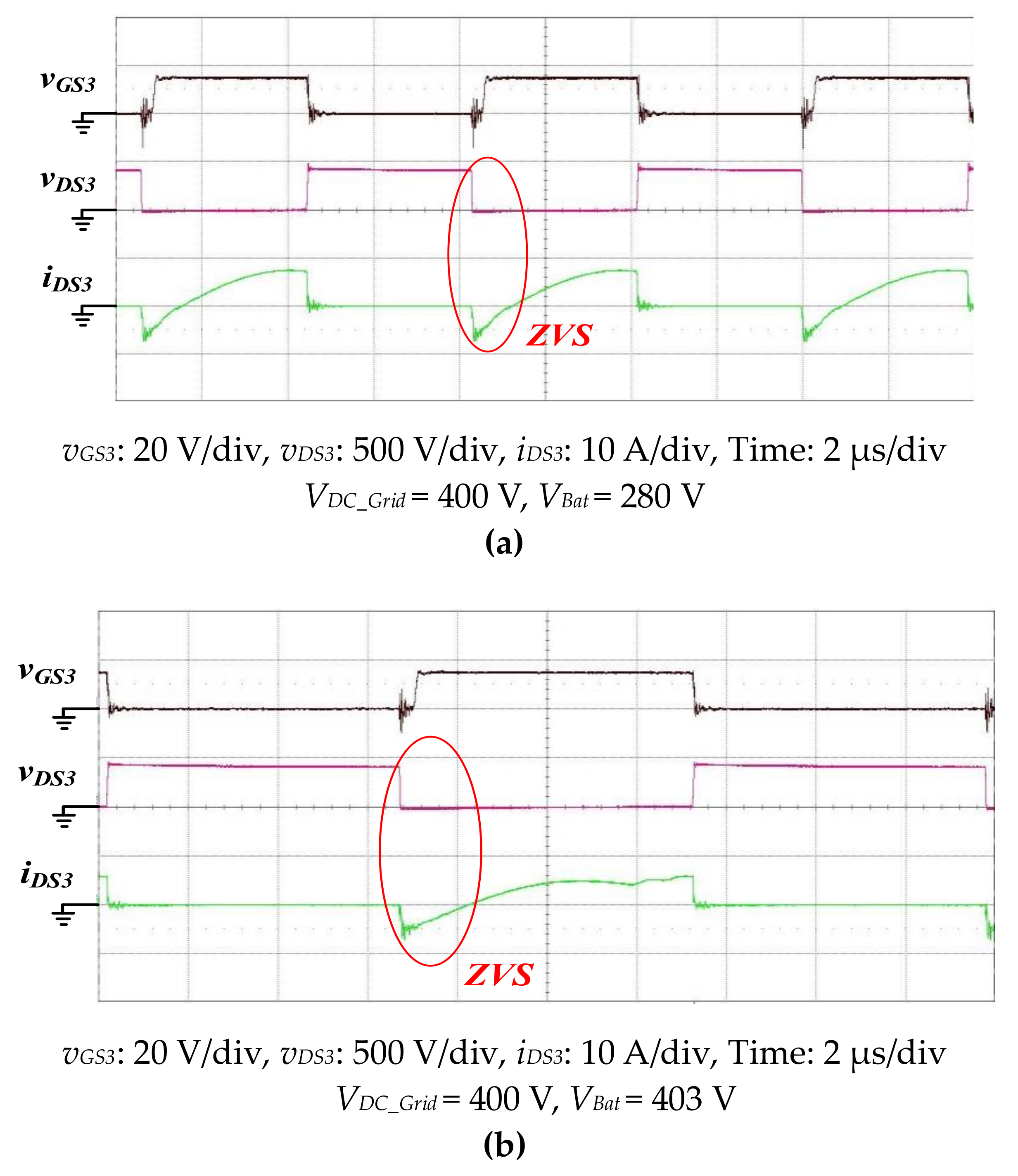
6.1. Critical Measurements for the Forward Charging Mode
Figure 16 shows the measurement results of
vGS3, vDS3, and
iDS3 in the cases where
VDC_Grid = 400 V and charging battery voltages are
VBat = 280 V and
VBat = 403 V respectively. It is obvious that there appears a reverse current
iDS3 inside the power switch both in
Figure 16a,b which helps remove the energy on the parasitic capacitance and rapidly decline
VDS3 to 0V, thus achieving ZVS.
Figure 17 shows the measurement results of
vDB7 and
iDB7 in the cases where
VDC_Grid = 400 V and charging battery voltages are
VBat = 280 V and
VBat = 403 V, respectively. By observing
Figure 17a, the diode current
iDB7 has not fallen to 0 A prior to the cut-off of diode D
B7 and thus leads to diode ZCS failure.
Figure 17b shows that the diode current
iDB7 has reached 0 A before diode
DB7 turns off and thus succeeds in the ZCS of
DB7. It is worth noting that the oscillation of
vDB7 at the switching instant resulted from the resonance of parasitic capacitance and resonant inductance.
6.2. Critical Measurements for the Reverse Discharging Mode
Figure 18 shows the measurement results of
vGS8,
vDS8, and
iDS8 in the cases where the discharging battery voltages are
VBat = 280 V and
VBat = 403 V, respectively, and
VDC_Grid = 400 V. It is obvious that there appears a reverse current
iDS8 inside the power switch both in
Figure 18a,b, which helps remove the energy on the parasitic capacitance and rapidly decline v
DS8 to 0 V, thus achieving ZVS.
Notably,
Figure 19a clearly exhibits the advantage of a symmetric dual resonant converter in that the voltage gain is obviously greater than 1.
Figure 19 shows the measurement results of
vDB4 and
iDB4 in the cases where the discharging battery voltages are
VBat = 280 V and 403 V, respectively, and the DC grid voltage
VDC_Grid = 400 V. By observing
Figure 19a, the diode current
iDB4 has fallen to 0 A prior to the cut-off of diode
DB4 and thus leads to diode ZCS being successful. It is worth noting that there appears oscillation of
vDB4 at the switching instant, which resulted from the resonance of parasitic capacitance and the secondary resonant inductance. Due to the resonant converter working at Region I,
Figure 19b shows that the diode current
iDB4 has not reached 0 A before diode
DB4 turns off and thus fails in ZCS of
DB4.
6.3. Efficiency Plots for Forward Mode and Reverse Mode
Figure 20 shows the efficiency curves with battery voltages
VBat being 280, 340, and 403 V and charging currents ranging from 0.5 to 2.5 A. This reveals that the maximum conversion efficiency is 91.96% at the lowest battery voltage 280 V, and the maximum conversion efficiency is 93.25% at the highest battery voltage 403 V. The maximal efficiency of 93.67% appears in the case of the 340 V battery voltage because it gets near to the resonant point, and the total impedance is nearly 0. In the forward charging mode, the voltage of DC grid is 400 V, and the designed resonant frequency is around 100 kHz at the 340 V battery voltage, thus getting higher efficiency due to the switching instants of the turn-on and cut-off being near the zero-crossing point. When the discharging current is low, although possessing both ZVS and ZCS, the effect is not obvious due to low current. As the current rises to 1.5A, the efficiency at battery voltage 403 V apparently surpasses that with 280 V battery voltage.
Figure 21 shows the efficiency curves with discharging voltages
VBat being 280, 340, and 403 V and discharging currents ranging from 0.5 to 2.5 A. In the reverse discharging mode, the voltage of DC grid is 400 V as well. For low battery voltage level, it needs more voltage gain to fulfill DC grid charging and operates in the Region II due to low operating frequency. At different voltage levels of the battery, low battery voltage conditions need more current to discharge the constant voltage DC grid to achieve the identical power level and thus experience more relative power loss. In the case of a 280 V battery voltage, despite the converter operating in Region II and possessing ZCS on the rectifier side, its power loss rate is relatively higher. Operating at a 340 V battery voltage, even though the converter works near the resonant frequency and possesses the advantage of ZVS and ZCS, the conversion efficiency is better than that of the 403 V battery voltage due to more discharging current being needed for the identical power conversion. In fact, when the battery voltage is 403 V and operates at high frequency in Region I with only a ZVS mechanism, it achieves similar efficiency with that of 340 V. This reveals that the maximum conversion efficiency is 91.3% at the lowest discharging voltage 280 V, and the maximum conversion efficiency is 94.6% at the highest discharging voltage 403 V.
7. Conclusions
This research accomplished and realized an isolated type bidirectional symmetric resonant converter with a wide voltage range. By modifying the traditional LLC resonant topology, the secondary side rectifying diodes were replaced by active power switches to constitute a dual active bridge topology. With the introduction of a second set of resonant devices to the secondary side, the symmetric structure enabled the voltage gain to be greater than 1. Indeed, the developed converter is featured with a wide voltage range due to symmetric topology and good conversion efficiency due to ZVS and ZCS functionality. Finally, a 1 kW bidirectional power flow converter that assigns one port with voltage 400 V and another port with voltage ranging from 280 to 403 V was accomplished. The measurements indicate that the maximum conversion efficiency can reach 93.25% in the forward charging mode and is as high as 94.60% in the reverse discharging mode.
Author Contributions
Y.-H.Y. conceived and designed the proposed resonant converter; Y.-N.C. performed the circuit simulation and designed the parameters of the converter components; Y.-D.C. carried out the prototype resonant converter and measured as well as analyzed the experimental results; S.-Y.C. wrote the paper, and H.-L.C. revised it for submission. All authors have read and agreed to the published version of the manuscript.
Funding
This research received no external funding.
Acknowledgments
This work was supported by the Ministry of Science and Technology, R.O.C. under the grant MOST 109-2221-E-150-021-MY2.
Conflicts of Interest
The authors declare no conflict of interest.
References
- Ma, Z.; Pesaran, A.; Gevorgian, V.; Gwinner, D.; Kramer, W. Energy storage, renewable power generation, and the grid: NREL capabilities help to develop and test energy-storage technologies. IEEE Electrif. Mag. 2015, 3, 30–40. [Google Scholar] [CrossRef]
- Babokany, A.S.; Jabbari, M.; Shahgholian, G.; Mahdavian, M. A review of bidirectional dual active bridge converter. In Proceedings of the 9th International Conference on Electrical Engineering/Electronics, Computer, Telecommunications and Information Technology; Institute of Electrical and Electronics Engineers (IEEE), Phetchaburi, Thailand, 16–18 May 2012; pp. 1–4. [Google Scholar]
- Tytelmaier, K.; Husev, O.; Veligorskyi, O.; Yershov, R. A review of non-isolated bidirectional dc-dc converters for energy storage systems. In Proceedings of the 2nd International Young Scientists Forum on Applied Physics and Engineering (YSF), Kharkiv, Ukraine, 10–14 October 2016; pp. 22–28. [Google Scholar]
- Zhao, B.; Yu, Q.; Sun, W. Bidirectional full-bridge DC-DC converters with dual phase-shifting control and its backflow power characteristic analysis. In Proceedings of the Chinese Society of Electrical Engineering, Bejing, China, 25 April 2012; pp. 43–50. [Google Scholar]
- Zhao, B.; Song, Q.; Liu, W. Efficiency Characterization and Optimization of Isolated Bidirectional DC–DC Converter Based on Dual-Phase-Shift Control for DC Distribution Application. IEEE Trans. Power Electron. 2013, 28, 1711–1727. [Google Scholar] [CrossRef]
- Zhao, B.; Song, Q.; Liu, W.; Sun, Y. Overview of dual-active-bridge isolated bidirectional DC–DC converter for high-frequency-link power-conversion system. IEEE Trans. Power Electron. 2013, 29, 4091–4106. [Google Scholar] [CrossRef]
- Li, W.; Zhao, H.; Kan, T.; Mi, C. Inter-operability considerations of the double-sided LCC compensated wireless charger for electric vehicle and plug-in hybrid electric vehicle applications. In Proceedings of the IEEE PELS Workshop on Emerging Technologies: Wireless Power (2015 WoW), Daejeon, Korea, 5–6 June 2015; pp. 1–6. [Google Scholar]
- Shafiei, N.; Saket, M.A.; Ordonez, M. Time domain analysis of LLC resonant converters in the boost mode for battery charger applications. In Proceedings of the IEEE Energy Conversion Congress and Exposition (ECCE), Cincinnati, OH, USA, 1–5 October 2017; pp. 4157–4162. [Google Scholar]
- Liu, C.; Wang, J.; Colombage, K.; Gould, C.; Sen, B. A CLLC resonant converter based bidirectional EV charger with maximum efficiency tracking. In Proceedings of the 8th IET International Conference on Power Electronics, Machines and Drives (PEMD 2016), Glasgow, UK, 19–21 April 2016; pp. 1–6. [Google Scholar]
- Dalala, Z.; Zahid, Z.U.; Saadeh, O.; Lai, J.S.J. Modeling and controller design of a bidirectional resonant converter battery charger. IEEE Access 2018, 6, 23338–23350. [Google Scholar] [CrossRef]
- Pledl, G.; Tauer, M.; Buecherl, D. Theory of operation, design procedure and simulation of a bidirectional LLC resonant converter for vehicular applications. In Proceedings of the IEEE Vehicle Power and Propulsion Conference, Lille, France, 1–3 September 2010; pp. 1–5. [Google Scholar]
- Chen, W.; Rong, P.; Lu, Z. Snubberless bidirectional DC–DC converter with new CLLC resonant tank featuring minimized switching loss. IEEE Trans. Ind. Electron. 2010, 57, 3075–3086. [Google Scholar] [CrossRef]
- Lv, Z.; Yan, X.; Fang, Y.; Sun, L. Mode analysis and optimum design of bidirectional CLLC resonant converter for high-frequency isolation of DC distribution systems. In Proceedings of the IEEE Energy Conversion Congress and Exposition (ECCE), Montreal, QC, Canada, 20–24 September 2015; pp. 1513–1520. [Google Scholar]
- Tan, K.; Yu, R.; Guo, S.; Huang, A.Q. Optimal design methodology of bidirectional LLC resonant DC/DC converter for solid state transformer application. In Proceedings of the 40th IEEE Annual Conference of the IEEE Industrial Electronics Society, Dallas, TX, USA, 29 October–1 November 2014; pp. 1657–1664. [Google Scholar]
- Jiang, T.; Zhang, J.; Wu, X.; Sheng, K.; Wang, Y. A Bidirectional LLC resonant converter with automatic forward and backward mode transition. IEEE Trans. Power Electron. 2015, 30, 757–770. [Google Scholar] [CrossRef]
- Zhang, J.; Liu, J.; Yang, J.; Zhao, N.; Wang, Y.; Zheng, T.Q. An LLC-LC type bidirectional control strategy for an LLC resonant converter in power electronic traction transformer. IEEE Trans. Ind. Electron. 2018, 65, 8595–8604. [Google Scholar] [CrossRef]
- Zong, S.; Fan, G.; Yang, X. Double Voltage Rectification Modulation for Bidirectional DC/DC Resonant Converters for Wide Voltage Range Operation. IEEE Trans. Power Electron. 2018, 34, 6510–6521. [Google Scholar] [CrossRef]
- Song, J.; Yang, D.; Zhang, C.; Duan, B. Hybrid control method for CLLLC resonant converter with Low output voltage ripple. IFAC PapersOnLine 2018, 51, 680–684. [Google Scholar] [CrossRef]
- Texas Instruments Power Supply Design Seminar. Designing an LLC Resonant Half-Bridge Power Converter; Texas Instruments Power Supply Design Seminar: Dallas, TX, USA, 2019. [Google Scholar]
- Ditze, S. Steady-state analysis of the bidirectional CLLLC resonant converter in time domain. In Proceedings of the IEEE 36th International Telecommunications Energy Conference (INTELEC), Vancouver, BC, Canada, 28 September–2 October 2014; pp. 1–9. [Google Scholar]
- Lu, B.; Liu, W.; Liang, Y.; Lee, F.; van Wyk, J. Optimal design methodology for LLC resonant converter. In Proceedings of the 21st Annual IEEE Applied Power Electronics Conference and Exposition, APEC’06, Dallas, TX, USA, 19–23 March 2006; pp. 533–538. [Google Scholar]
- Luo, S.J. Implementation of a Dual-Active-Bridge Bidirectional Isolated DC to DC Converter in Home Area Network. Master’s Thesis, Department of Electrical Engineering, National Sun Yat-Sen University, Kaohsiung City, Taiwan, 2012. [Google Scholar]
- Liang, J.C. Contactless Li-Mn Battery Charger with Intelligent Control. Master’s Thesis, Department of Electrical Engineering, National Central University, Taoyuan City, Taiwan, 2014. [Google Scholar]
Figure 1.
The proposed isolated bidirectional symmetric resonant converter with dual active full bridge.
Figure 1.
The proposed isolated bidirectional symmetric resonant converter with dual active full bridge.
Figure 2.
Voltage gain of LLC resonant converter at forward and reverse modes.
Figure 2.
Voltage gain of LLC resonant converter at forward and reverse modes.
Figure 3.
Voltage gain profile in the forward mode of the proposed bidirectional symmetric resonant converter.
Figure 3.
Voltage gain profile in the forward mode of the proposed bidirectional symmetric resonant converter.
Figure 4.
Power propagation of the forward charging mode.
Figure 4.
Power propagation of the forward charging mode.
Figure 5.
Important theoretic waveforms operating in Region II.
Figure 5.
Important theoretic waveforms operating in Region II.
Figure 6.
The conduction path of each stage in Region II: (a) Stage I conduction path; (b) Stage II conduction path; (c) Stage III conduction path; (d) Stage IV conduction path; (e) Stage V conduction path.
Figure 6.
The conduction path of each stage in Region II: (a) Stage I conduction path; (b) Stage II conduction path; (c) Stage III conduction path; (d) Stage IV conduction path; (e) Stage V conduction path.
Figure 7.
AC equivalent circuit of converter in the forward operation.
Figure 7.
AC equivalent circuit of converter in the forward operation.
Figure 8.
AC equivalent circuit of converter in the reverse operation.
Figure 8.
AC equivalent circuit of converter in the reverse operation.
Figure 9.
The design flowchart of bidirectional symmetric resonant converter.
Figure 9.
The design flowchart of bidirectional symmetric resonant converter.
Figure 10.
Voltage gain curves with different Q1 and fixed k1, g1, and m1.
Figure 10.
Voltage gain curves with different Q1 and fixed k1, g1, and m1.
Figure 11.
The voltage gain curves operating in the forward charging mode.
Figure 11.
The voltage gain curves operating in the forward charging mode.
Figure 12.
The voltage gain curves operating in the forward and reverse charging modes.
Figure 12.
The voltage gain curves operating in the forward and reverse charging modes.
Figure 13.
The overall system structure of the isolated bidirectional symmetric resonant converter.
Figure 13.
The overall system structure of the isolated bidirectional symmetric resonant converter.
Figure 14.
The functional block diagram of the battery storage.
Figure 14.
The functional block diagram of the battery storage.
Figure 15.
The voltage state under abrupt load current fluctuation: (a) load current changes from 1.5 A to 2.5 A; (b) load current changes from 2.5 A to 1.5 A.
Figure 15.
The voltage state under abrupt load current fluctuation: (a) load current changes from 1.5 A to 2.5 A; (b) load current changes from 2.5 A to 1.5 A.
Figure 16.
Waveforms of vGS3, vDS3, and iDS3 with two battery voltages: (a) VBat = 280 V; (b) VBat = 403 V.
Figure 16.
Waveforms of vGS3, vDS3, and iDS3 with two battery voltages: (a) VBat = 280 V; (b) VBat = 403 V.
Figure 17.
Waveforms of vDB7 and iDB7 with two battery voltages: (a) VBat = 280 V; (b) VBat = 403 V.
Figure 17.
Waveforms of vDB7 and iDB7 with two battery voltages: (a) VBat = 280 V; (b) VBat = 403 V.
Figure 18.
Waveforms of vGS8, vDS8, and iDS8 with two discharging battery voltages: (a) VBat = 280 V; (b) VBat = 403 V.
Figure 18.
Waveforms of vGS8, vDS8, and iDS8 with two discharging battery voltages: (a) VBat = 280 V; (b) VBat = 403 V.
Figure 19.
Waveforms of vDB4 and iDB4 with two discharging battery voltages: (a) VBat = 280 V; (b) VBat = 403 V.
Figure 19.
Waveforms of vDB4 and iDB4 with two discharging battery voltages: (a) VBat = 280 V; (b) VBat = 403 V.
Figure 20.
Conversion efficiency curves for the forward charging mode.
Figure 20.
Conversion efficiency curves for the forward charging mode.
Figure 21.
Conversion efficiency curves for the reverse discharging mode.
Figure 21.
Conversion efficiency curves for the reverse discharging mode.
Table 1.
Converter specifications.
Table 1.
Converter specifications.
| Parameters | Specifications |
|---|
| DC grid voltage VDC_Grid | 400 V |
| Battery port voltage VBat | 280–403 V |
| Max. conversion power P | 1000 W |
| Series resonant frequency fr1 | 100 kHz |
| Power switching range fs | 70–150 kHz |
Table 2.
Selected parameters of the important devices.
Table 2.
Selected parameters of the important devices.
| Device Symbol | Quantity |
|---|
| Transformer turn ratio NP:NS | 1.2:1 |
| Magnetizing inductance Lm | 219.85 µH |
Resonant inductance Lr1
(including primary leakage inductance) | 61.2 µH |
Resonant inductance Lr2
(including secondary leakage inductance) | 44.36 µH |
| Resonant capacitance (primary) Cr1 | 41.4 nF |
| Resonant capacitance (secondary) Cr2 | 53.7 nF |
| DC grid capacitor tank CDC_Grid | 540 µF |
| Battery capacitor tank CBat | 540 µF |
| Power switches Q1–Q8 | C2M0160120D |
| Trigger controller | TMS320F28335 |
| Publisher’s Note: MDPI stays neutral with regard to jurisdictional claims in published maps and institutional affiliations. |
© 2020 by the authors. Licensee MDPI, Basel, Switzerland. This article is an open access article distributed under the terms and conditions of the Creative Commons Attribution (CC BY) license (http://creativecommons.org/licenses/by/4.0/).


